2016 IEEE 36th International Conference on Electronics and Nanotechnology (ELNANO)
128
Investigation of Native Oxide Removing from
HCPA ALD Grown GaN Thin Films Surface
Utilizing HF Solutions
Petro Deminskyi, Ali Haider, Necmi BiyikliUNAM Bilkent University Ankara, Turkey [email protected], [email protected], [email protected]
Alexander Ovsianitsky, Alexander Tsymbalenko, Dmitry Kotov, Vladyslav Matkivskyi, Nata Liakhova, Vladimir Osinsky
Research Institute of microdevices, National Academy of Science of Ukraine
Kiev, Ukraine
[email protected], [email protected], [email protected], [email protected],
[email protected], [email protected] Abstract — The paper consider oxygen contamination of
HCPA ALD grown GaN films under an air conditioning and during different time duration. High resolution XPS analysis of HCPA ALD grown GaN films after diluted 1:10 HF(41 %) : H2O and undiluted HF (41 %) influence on oxygen impurities was investigated. Lesser oxygen impurities have been observed. Better resistivity to oxygen atoms of GaN thin films after diluted HF solution treatment was achieved compared to undiluted HF treatment and without treatment.
Keywords — GaN; HCPA ALD; oxygen; contamination; thin films. I. INTRODUCTION
III-Nitrides (Al, In, Ga)N — are excellent semiconductor compounds, which are of significant research attention over the last 20–25 years. Their properties [1-5] such as wide energy bandgap, high electron saturation velocity, high breakdown fields, high operational temperatures, low thermal generation rates, radiation tolerance and biocompatibility led to many highly successful technologies in the electronic and photonic systems [6] (high power LED's [7], HEMT’s [8, 9], multijunction solar cells [10, 11], future optical and memory devices, FETs, HEMTs and sensors [12], etc.).
Currently, atomic layer deposition (ALD) is one of the most promising low-temperature nanometric deposition techniques. It offers to obtain high conformal coatings even on very complex tridimensional surfaces, with a strict thickness tolerance. During an ALD cycle, only one molecular layer is deposited on the substrate surface, enabling the theoretical possibility to tailor the composition of the deposit up to molecular resolution [13]. The importance of ALD processes for high throughput and coating on complex device geometries is well recognized for these applications. Nevertheless this technique it still has to be improved for III-N compounds and their ternary solutions for obtaining better crystalline structures.
Moreover, there are still a lot of challenges that have to be solved for obtaining better crystalline structures and device
quality layers: oxygen and carbon contamination [14], limited conformality [15], uniform doping [16], slowness of the process and others. Contamination of achieved films by carbon and oxygen is a challenging problem. This issue may exist because of insufficient purity of source gases and background contaminants in the vacuum. Oxygen contamination can also result from ex-situ exposure to air for polycrystalline materials. The existence of the native oxide layer on the air-exposed surface implied the possible creation of an uncontrolled dislocation formation that might significantly affect the next steps of a device fabrication process. It is one of the reasons of high densities of the threading dislocation (TDs) during GaN layer growth [17]. It can cause serious degradation processes in devices right up to complete failure of them.
Due to the necessity of transferring the samples from one tool to another, it is critical to protect atomic layer deposited films from atmospheric oxidation. A number of methods can help in solving the problem of contamination, among them are: HF treatment, annealing, capping layers [18], exposure to the H2 flux [19], etc. Additionally, this pollution can be addressed with gas purifiers, and by improving the vacuum system with the use of load locks, adequate attention to system leaks and having a good quality pumping system. Substituting alumina tubes for quartz can lead to some improvement [20].
Thus, our main goals is to understand: (1) how could we efficiently remove native oxide from the surface of III-nitride thin films grown using hollow cathode plasma assisted ALD; (2) how and for how long could we protect the film surfaces from oxidation for the next steps of device fabrication.
Previously reported results [21] provide evidence to believe that our further experiments will allow us to obtain III-nitride thin films grown using hollow cathode plasma assisted ALD that could be more stable to the outer environment after HF-treatment. Due to previous study of HF, HCl (at room temperature) and NH4OH (at 50 °C) treatments of MOCVD InAlN films [22], we used only HF solution in our experiments.
2016 IEEE 36th International Conference on Electronics and Nanotechnology (ELNANO)
129 II. EXPERIMENTAL
Gallium nitride film were deposited on Si (100) substrate at growth temperature 200 °C by using a Fiji LL Cambridge Nanotech ALD reactor equipped with remote inductively coupled RF-power source and base pressure 0.2 Torr. We used GaEt3 as a metal-organic precursor for Ga source. Ar is used as the carrier and plasma gas with 30 and 100 sccm flow rates for GaEt3 and N2/H2 flows, respectively. A total of 1000 growth cycles were carried out at 300 W plasma power [23]. Film thickness and refractive index were estimated by using a visible range variable angle spectroscopic ellipsometry (SE) at three angles of incidence (ȥ (65, 70, 75), ǻ). The refractive index and thickness of GaN grown film were extracted from SE data by using the Cauchy dispersion function. Both undiluted (41 %) and diluted (1:10 of 41%) HF treatment of GaN films during 1min at room temperature was used for our study. For better comparative results free of treatment GaN film was additionally used. For better understanding what is the effect of HF on GaN samples, we checked oxide contamination after 10 min, 20 min, 30 min, 1 hour, 2 hours and 1 week of undiluted, diluted HF treatment and after the same periods of time for GaN film right after ALD growth without HF treatment. The elemental profiles and impurity incorporation of the GaN films after undiluted, diluted HF treatment and right after ALD growth were determined by X-ray photoelectron spectroscopy (XPS) operating at monochromatized Al Ka wavelength.
III. RESULTS AND DISCUSSION
We explored the influence of HF treatment on the oxygen contamination of GaN films. The initial results for diluted HF treatment of GaN during 1 and 2 minutes still show presence of O1s after HF treatment that might be caused by oxygen diffusion inside few layers of GaN along the interface of air/GaN. Oxygen contamination on the surface was better for the sample which was treated with diluted HF during 1 minutes (7,33 %) comparing with sample after 2 minutes of HF treatment (8,33 %) (see Table 1).
These contaminations differences between these two peaks might be caused by the different speed of GaN surface degradation during diluted and undiluted HF treatment that under a longer time make the surface after 2 min more non-uniform. Larger HF concentration might be a main reason of surface area increasing that lead to a faster oxidation under an air conditions. That is why for our further study we used HF treatment of GaN film during 1 minute.
The XPS O1s spectral intensity of GaN was reduced efficiently by HF-based solution at room temperature, compared with the sample without HF treatment (Table. 1). Because the oxide is removed mainly by HF, F1s group are also present.
The next aim of our study lies in characterization of surface oxidizing and oxygen contamination of GaN samples, after 10 min, 20 min, 30 min, 1 hour, one week of HF treatment of GaN film surface.
TABLE I. ATOMIC % OF GA3D,O1S,F1S,C1S AND N1S GROUPS AFTER
1 MIN HF TREATMENT OF GAN AND 10 MIN PRESENCE ON THE AIR ʋ Name Atomic % (without HF treatment) Atomic % (1 min HF treatment) Atomic % (2 min HF treatment) 1. Ga3d 30,63 24,91 24,77 2. O1s 4,48 7,33 8,33 3. F1s - 4,1 3,87 4. C1s - 8,51 8,73 5. N1s 63,97 55,14 54,31
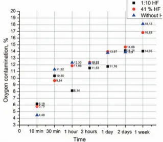
Figure 1 shows the difference in oxygen contamination for GaN film after different periods of time. We can make several observations on obtained results:
- 41% HF, 1:10 41% HF treat GaN film surface in a different ways. While 41% HF removing the oxygen more effectively and open more ALD GaN surfaces, 1:10 41% HF less active for GaN surface treatment; GaN film right after ALD growth process is more stable to the oxygen influence compared with 41% HF, 1:10 41% HF
- 10 minutes after HF treatment both GaN samples in 41% HF and 1:10 41% HF solutions have almost equal percentage of oxygen on the surface. Lower percentage of oxygen without HF is due to the XPS characterization of the sample immediately after ALD grown GaN that show more resistant stable to the oxidation processes under the air conditions;
- 30 minutes after HF treatment GaN sample in 41% HF solution show lower oxygen contamination due to more effective oxygen removing from the sample and not long time duration after HF treatment. Oxygen contamination in the sample without HF treatment start to increase faster compared to two other samples;
- 1, 2 hours, 1 day, 1 week after HF treatment GaN sample in 1:10 41% HF solution (compared with sample treated in undiluted HF solution) show better stability under air conditioning. After this point we see almost the same correspondences.
2016 IEEE 36th International Conference on Electronics and Nanotechnology (ELNANO)
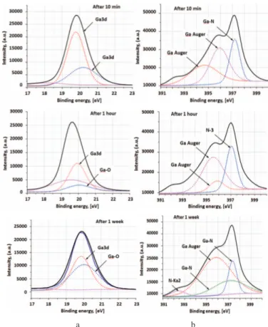
130 As far as 1:10 HF solution seems the best choice for getting more resistant GaN top surface, we obtained high resolutions Ga3d, O1s and N1s peaks via XPS system and made parameters fitting of the surface of samples that were treated with 1:10 HF solution and their air conditioning during 10 min, 1 hour and 1 week. For sample after 10 min under air conditioning we observe the main peak and first sub peak that reveals Ga3d signal on the surface. The second sub peak is 20.19 eV. This binding energy still related to Ga3d, nevertheless this slight shift to higher energy show initial surface modification with oxygen. In the literature Ga2O3 expected to be centered at 20.5 eV or higher [24] that confirm our hypothesis. The XPS spectra show O1s peak on 531.07 eV and coincide with literature [25].
The Ga3d and O1s XPS analysis of GaN sample after 1 hour of 1:10 HF treatment reveal a dominant subpeak at 532.48±0.1 eV, that corresponds to O-C peak (due to atmospheric contamination) that closely similar to a literature data (532.6 eV) [26, 27] and binding energy ∼19.68 eV that represent narrow Ga3d signal. The presence of peak in a binding energy 20.07 eV start to appear, that represent Ga-O binding [28], while second sub peak 19.94 eV increase in intensity. This sub peak might reveal to a second sub peak from samples with 10 min of air conditioning.
Ga3d XPS analysis of GaN sample after 1 week of 1:10 HF treatment reveal a dominant subpeak at 532.48±0.1 eV and binding energies at 19.8 eV and 20.07 eV, that represent Ga-O bond and larger shifting to bigger energies, compared to 1 hour of 1:10 HF treatment of GaN film that related to Ga2O3. As we can see from Fig. 2a (After 1 week), Ga-O binding peak increase, while intensity of Ga3d decreasing.
High resolution XPS scan of N1s was collected to obtain oxidation state information about GaN film. The N 1s peak is commonly used for the identification of the nitrogen oxidation state. This is due to its high photoemission intensity [29]. The main peak that was obtained both after 10 min 397.18 eV Ga-N binding [30] and 1 hour was 397.02 eV that correspond to N-3 and represent nitride [31]. As seen in Fig. 2, another N1s peak is centered at 397.7 eV, which corresponds to the nitride oxidation state [32]. Peak at 395.7 eV correspond to Ga Auger peaks [33]. Relative energy binding show slight shifting in intensity for 10 min and 1 hour (400 a.u.) while intensity comparison for samples after 10 min and 1 week under air conditions show decreasing in intensity up to 1150 a.u. For main peaks that related to N1s and Ga-N binding intensity decrease, while intensity of sub peaks increasing.
CONCLUSION
After detailed study of native oxide presence in GaN thin films after HF treatment and comparatively inconsiderable time under the air conditioning (10 min) we observed top GaN layers still contain ∼3–6 % of oxide atoms depending on HF concentration and HF treatment time. Better resistivity was observed for GaN film without any HF treatment 10 min after HCPA ALD grown GaN. The resistivity of GaN film to oxygen incorporation decrease after enlargement of air conditioning time for samples (1) without and (2) with undiluted HF treatment.,
while for sample with utilization of diluted HF, GaN surface becomes more resistive in comparison to previous samples.
a b
Fig. 2. High-resolution XPS spectra of (a) Ga3d and (b) N1s peaks of PEALD grown GaN films after different time of air conditioning.
GaN films after diluted 1:10 HF treatment of top surface show better resistivity to the air incorporation after 30 min, 1 hour, 2 hours and 1 week under air influence that might be caused because of top surface oxygen saturation and better packaging of underneath GaN film.
HCPA ALD GaN grown films could be used for further technological steps where oxygen contamination on the surface in the range to 5-10 % is not critical. Otherwise, other technological optimization steps for better resistivity or improved technique for native oxide removing from the top GaN are needed.
ACKNOWLEDGMENT
The This work was performed at UNAM under “2216 – research fellowship program for international researchers” gratefully acknowledges the financial support from TUBITAK, UNAM, Institute of Material Science and Nanotechnology.
REFERENCES
[1] Simin G, Hu X, Ilinskaya N, et al. Large periphery high-power AlGaN/GaN metal-oxide-semiconductor heterostructure field effect transistors on SiC with oxide-bridging. IEEE Electron Device Lett, 2001, 22(2): 53
[2] Daumiller I, Theron D, Gaquiere C, et a1. Current instabilities in GaN-based devices. IEEE Electron Device Lett, 2001, 22(2): 62
2016 IEEE 36th International Conference on Electronics and Nanotechnology (ELNANO)
131
[3] Mishra U K, Zolper J C. Special issue on group III–V semiconductor electronics. IEEE Trans Electron Devices, 2001, 48: 405
[4] Wu Y F, Kapolnek D, Ibbetson J P, et al. Very-high power density AlGaN/GaN HEMTs. IEEE Trans Electron Devices, 2001, 48(3): 586 [5] N. Tsurumi, et al., “GaN Transistors for Power Switching and High
Frequency Applications”, Digest of Papers from the 2008 Compound Semiconductor and Circuits Symposium, pp. 1–5.
[6] Perspectives on future directions in III-N semiconductor research Charles R. Eddy Jr.1,a), Neeraj Nepal2,b), Jennifer K. Hite3 andMichael A. Mastro3
[7] V.I. Osinsky, P.V. Deminsky, etc. 8th All-Russian Conference "Gallium, aluminum and indium nitrides", St-Petersburg, Russia (2011)
[8] S. Tripathy, V. K. X. Lin, etc. Appl. Phys. Lett. 101 (8), 082110 (2012). [9] K. Radhakrishnan, N. Dharmarasu, Appl. Phys. Lett. 97 (23), 232107 (2010). [10] Jian-Wei Ho Journal of Crystal Growth 420, 64–73 (2015)
[11] Macho Microelectronics Journal 40, 427– 434 (2009)
[12] Elia Marin, Alex Lanzutti, Francesco Andreatta, Maria Lekka, Luis Guzman, Lorenzo Fedrizzi, Corrosion Reviews Volume 29, Issue 5-6 (Nov 2011) Atomic layer deposition: state-of-the-art and research/industrial perspectives
[13] Anjana Devi, Volume 257, Issues 23–24, December 2013, Pages 3332– 3384, ‘Old Chemistries’ for new applications: Perspectives for development of precursors for MOCVD and ALD applications
[14] J. Musschoot , Q. Xie, D. Deduytsche , S. Van den Berghe, R.L. Van Meirhaeghe, C. Detavernier, Microelectronic Engineering 86 (2009) 72– 77 Atomic layer deposition of titanium nitride from TDMAT precursor [15] Nicola Pinna,Mato Knez Atomic Layer Deposition of Nanostructured
Materials p.67
[16] Lauri Niinistö, Atomic Layer Deposition of Rare Earth Oxides, Helsinki University of Technology p. 6
[17] E. A. Stach Appl. Phys. Lett. 79, 335 (2001)
[18] Chung-Mo Yang et al 2007 Jpn. J. Appl. Phys. 46 1981
[19] Interaction Between Plasma and Low-kappa Dielectric Materials, ProQuest, 2008, p.174
[20] N. M. Johnson, J. Walker, C. M. Doland, K. Winer and R. A. Street, Appl. Phys. Lett. 54 (1989) 1872.
[21] M. Akazawa, M. Chiba, and T. Nakano. CS MANTECH Conference, Denver, Colorado, USA (2014)
[22] Akazawa M., Chiba M., Nakano T. Process-dependent properties of InAlN surface and ALD-Al2O3/InAlN interface CS MANTECH Conference, May 19th - 22nd, 2014, Denver, Colorado, USA
[23] M. Alevli, A. Haider, S. Kizir, S. A. Leghari, and N. Biyikli, J. Vac. Sci. Technol. A 34, 01A137 (2016).
[24] Giroire B., Marre S. Garcia A. Cardinal T., Aymonier C. Continuous supercritical route for quantum-confined GaN nanoparticles / The Royal Society of Chemistry, 2015
[25] SaygÕlÕa H., Fuat Güzelb F. J. Chemical engineering research and design 100 27–38, (2015)
[26] NIST X-ray Photoelectron Spectroscopy Database, National Institute of Standards and Technology, http://srdata.nist.gov/XPS/
[27] P. Y. Jouan, M. C. Peignon, C. H. Cardinaud, G. Lemperiere, “Characterisation of TiN coatings and of the TiN/Si interface by x-ray photoelectron spectroscopy and Auger electron spectroscopy”, Appl. Surf. Science, Vol.68, P.595 (1993).
[28] S. C. Ghosh, M. C. Biesinger, R. R. LaPierre, P. Kruse X-ray photoelectron spectroscopic study of the formation of catalytic gold nanoparticles on ultraviolet-ozone oxidized GaAs (100) substrates
Ă JOURNAL OF APPLIED PHYSICS 101, 114322 2007
[29] Vasile M.J., Emerson A.D. Baiocchi F.A. "Growth and Characterization of Thin Titanium Nitride Films," J. Vac. Sci. Tech., A8, 99-105 (1990) [30] Wei et al. Nanoscale Research Letters 2012, 7:562
[31] Kirkland W. Vogt and Paul A. Kohl Nitridation and CVD Reactions with Hydrazine / AIChE Journal, Vol 41, No 1, 1995
[32] Hedman J. Martensson N. Gallium nitride studied by electron spectroscopy. Phys. Scr., 22, 176 (1980)
[33] Kirste R., Rohrbaugh N., et al. Electronic Biosensors Based on III-Nitride Semiconductors Annual Review of Analytical Chemistry Vol. 8: 149-169 (Volume publication date July 2015)