https://doi.org/10.1007/s10854-019-02578-1
Identifying of series resistance and interface states
on rhenium/n‑GaAs structures using C–V–T and G/ω–V–T
characteristics in frequency ranged 50 kHz to 5 MHz
Osman Çiçek1 · Haziret Durmuş2 · Şemsettin Altındal3
Received: 15 October 2019 / Accepted: 12 November 2019 / Published online: 21 November 2019 © Springer Science+Business Media, LLC, part of Springer Nature 2019
Abstract
In this study, Re/n-GaAs with a native oxide layer based on metal–semiconductor (MS) structures were produced and then, the capacitance–voltage–temperature (C–V–T) and the conductance–voltage–temperature (G/ω–V–T) data of them were obtained in the frequency ranged 50 kHz to 5 MHz. Using the raw data, the electronic parameters was calculated by the developed LabVIEW-based program. Methodologically, the series resistance (Rs) values were calculated from the measured capacitance (Cm) and conductivity (Gm) values, while the interface state (Nss) values were obtained from using the combined high (CHF)–low (CLF) frequency capacitance method by Nicollian and Brews. Experimentally, the C values increased with a
decreasing frequency, while decreased with increasing temperatures in the depletion and accumulation regions. On the other hand, G/ω values decreased with increasing frequency in forward and reverse bias regions. It can be attributed that, the C and the G/ω values are quite affected by the presence of the Rs and the Nss in the forbidden energy gap and a native oxide layer between M and S. The Rs–V–T curves have especially peaks in accumulation and depletion regions at low frequency values,
whereas these peaks decreased at high frequencies. In addition, the Nss–V–T curves give peaks in the range of − 0.1 V to 0.7 V
at variable temperatures and the Nss values decrease with increasing temperature and shift towards negative bias regions. Experimental results indicate that the Rs and Nss are important parameters and so, these parameters must be considered in sensor applications based on Re/n-GaAs structures.
1 Introduction
Many scientists have tried to make electronic and opto-electronic devices such as sensors, field-effect transistors, integrated circuit devices, etc. based on metal–semiconduc-tor (MS) structures with and without a native oxide layer
or organic/inorganic layer as interfacial to increase their performance and reliability [1–6]. However, even if these structures have been studied for a long time, the temper-ature-dependent conduction mechanisms, which are dif-ferent than the expected condition in ideal, with difdif-ferent Schottky contact structures have not yet been investigated in detail. Additionally, in general, these studies were car-ried out only at one or narrow frequency, temperature and voltage range. But, these only at one or narrow temperature and frequency range cannot supply enough information to us on the conduction mechanism, the nature of BH at M/S interface, hopping, and polarization mechanisms. Therefore, in this study, both the temperature and frequency-dependent impedance measurement were carried out in wide range of temperature (90–400 K), frequency (50 kHz–5 MHz), and voltage ((− 2 V)–(3 V)) to get more and more reliable and confidence results on the conduction mechanisms, the for-mation of BH, and other electrical parameters.
Understanding of these structures is possible by obtaining the appropriate contact structure on the semiconductor as well as investigating the conductivity properties of a native
* Osman Çiçek [email protected] Haziret Durmuş [email protected] Şemsettin Altındal [email protected]
1 Department of Electrical and Electronics Engineering, Faculty of Engineering and Architecture, Kastamonu University, 37210 Kastamonu, Turkey
2 Physics Department, Faculty of Sciences, Selçuk University, Konya, Turkey
3 Physics Department, Faculty of Sciences, Gazi University, Ankara, Turkey
oxide or organic/inorganic insulator and semiconductor crys-tals [7]. Thus, as semiconductor crystal, gallium arsenide (GaAs) is a suitable material, which has been widely used in many applications, owing to very desirable electrical and optical properties for instance low power dissipation, high carrier mobility, and its direct bandgap [8–11].
As a rectifier contact, rhenium (Re) is a silvery metal, which is among the rarest metals in the world and does not form minerals of its own in nature. It is also the third-highest melting point after the materials of carbon and tungsten. On the other hand, it is preferred as an electrical contact mate-rial in electronic applications because it withstands wear and arc corrosion. In addition, Re is the one of the most suitable material for MS-based applications in high temperatures, because it is a thermodynamically stable metal when formed as tight contact with the semiconductor [12]. Hence, this study is the original owing to the fact that the Re metal recti-fier contact is untreated for MS structures and the investiga-tion of the capacitance–voltage–temperature (C–V–T) and the conductance–voltage–temperature (G/ω–V–T) charac-teristics of them in the wide frequency range.
In reality, the prescience of a native oxide layer or organic/inorganic layer between MS effects of the electronic parameters of MS structures [13, 14]. Moreover, the C–V and G/ω–V values of the MS structure in the ideal case are independent of the frequency, whereas the insulating layer between the MS, interface state density (Nss), series
resist-ance (RS), barrier height ( 𝛷B ), the ac signal frequency etc.
affect to the values of them in the application [15, 16]. Espe-cially, the C values for high frequencies (f ≥ 1 MHz) indicate a decrease in forward bias voltages, whereas this situation is different at low frequencies and temperatures [17–19]. Fur-thermore, the C–V and G/ω–V measurements of a MS-based device at a certain temperature do not provide the detailed information about its electronic parameters for instance the 𝛷B , RS, Nss, the concentration of donor atoms (ND), the
depletion-layer width (WD) etc. Therefore, the device should
be examined at a wide temperature range.
In the present study, Re/n-GaAs with a native oxide layer based on MS structures were fabricated to enhance their properties according to similar structures. In addition, the electronic parameters using the developed LabVIEW-based program was calculated from raw data of C–V–T and
G/ω–V–T measurements in the frequency range from 50 kHz
to 5 MHz. The effects of Rs, Nss, and the oxide layer between
Re and GaAs were investigated under different temperature and frequency. The Nss profile in the study was also
cal-culated by the combined high (CHF)–low (CLF) frequency
capacitance method.
2 Experimental procedure
Experimentally, Re/n-GaAs with a native oxide layer based on MS structures were prepared using rhenium (Re) as rectifier contact and n-type GaAs as a semiconductor. In this study, firstly, n-type GaAs substrate, which has two sides polished, [100] surface orientation, 4″ diam-eter, 0.625 mm thickness, 2.2–3.1 × 1018cm−3 doping
con-centration of donor atoms (Si), and, (1600–2130) cm2/V s
mobility, was supplied and cut into a dimension of about 10 mm × 10 mm as pieces. In terms of the reliability of the measurements and the obtained results, the substrate was cleaned with the most widely used procedure in the literature. Secondly, gold (Au) material with 99.9% purity was evaporated onto a back side of n-Si substrate using the thermal evaporating system in high-vacuum level at about 10−6 Torr to obtain about 150–200 nm thickness and then,
was annealed at 550 °C for getting low resistivity contact, i.e., ohmic contact. After that, Re material with 99.9% purity was coated onto a front side of the substrate using Pulsed Laser Deposition technique at about 10−7 Torr
for 2 h to get rectifier contact with 1.5 mm diameter or 0.0177 cm2 rectifier contact area and about 200–250 nm
thickness. The Re/n-GaAs with a native oxide layer based on MS structures were finished as ready for measure-ment, and also the schematic figures of them were given in Fig. 1a. In addition, it can be found in Reference [20] for more information about experimental procedures [20].
C–V–T characteristics and G/ω–V–T characteristics of
Re/n-GaAs type MS structures under different frequen-cies (50 kHz–5 MHz) were measured with 30 mV OSC level from − 4.0 to + 7.0 V in 50 mV steps using Hewlett Packard 4192A LF impedance analyzer. Lastly, electronic parameters using the developed LabVIEW-based program were calculated from raw data of C–V–T and G/ω–V–T measurements to analyze the performances of MS struc-tures. Additionally, more information about this calcula-tion methodology was explained in Reference [21].
3 Results and discussion
Barrier height ( 𝛷B ) is a highly considerable parameter
related to the work functions of metal ( 𝛷m ) and
semicon-ductor (𝛷s
)
, because the ideality of the device on elec-tronic behaviors is affected. Electrons with higher energy flow from semiconductor (S) side to metal (M) until the fermi energy levels (EF) are equal, when M–S junction,
which is defined as MS structure with organic/inorganic or a native oxide layer between M and S, is formed. In the case of thermal equilibrium, the conduction (EC) and
valence (EV) energy band edges are bent as in Fig. 1b,
because EF is completely constant and the forbidden
energy gap (Eg) or bandgap does not change. Here, the built-in voltage qVbi is equal to the difference between the
work functions of M and S materials ( qVbi= 𝛷m− 𝛷s ).
In other words, the barrier height of charges that pass from M to S is 𝛷B= 𝛷m− 𝜒s , while the potential barrier
height of charges that pass from S to M is qVbi. In addition,
𝛷B= qVbi+ EF can be written according to Fig. 1b [3].
C–V characteristics of MS structures supply more
infor-mation about their electronic parameters. Especially, inter-face state density Nss between M and S from C–V curves,
𝛷B and carrier concentration in semiconductor calculated
from the reverse bias C−2–V characteristics can be
calcu-lated for MS structures [15].
“C–V–T characteristics of Re/n-GaAs type MS struc-tures for four different frequencies (50 kHz, 100 kHz, 200 kHz, and 5 MHz) in the wide range of temperature (90–400 K) and voltage ((− 2 V)–(3 V)) were given in Fig. 2. Herein, it is clearly seen that the C values depend significantly on the temperature at variable frequencies. According to the applied gate voltage VG to the metal
side, the regions of inversion (VG≪ 0), depletion (VG> 0), and accumulation (VG ≫ 0) are clearly seen in each of the
C–V–T curves. The distinctions in the C–V–T values for
the variable frequencies are especially in the depletion and strong accumulation regions. This can be attributed to the presence of the Rs and the Nss in the forbidden energy gap
and a native oxide layer between M and S [15].
On the other hand, as can be seen below from the char-acteristics of the C–V–T, the C values exhibit an increasing behavior, especially with a decreasing frequency in the depletion regions, and these curves give a peak at about 0.5 V. According to Sands et al., in the strong accumu-lation regions (VG ≫ 0), the decrease in C–V–T curves at variable frequencies attributes the presence of series resistance (Rs) [22].
In the ideal case, both the C and G values of the MS structure with native and deposited an interfacial insulator, ferroelectric, and organic layer is usually independent at high frequencies limit, but the situation is different espe-cially at low or moderate frequencies due to the effects of Nss or dislocation localized at M/S interface, and Rs
of structure [14–19]. While, Nss can be usually generated by unsaturated dangling bonds of the surface atoms and some organic contaminations in laboratory environment, but Rs arise from due to the ohmic and rectifier contacts,
probe wire to the gate, particulate matter between the back contact and the pedestal, resistance of bulk semiconduc-tor, and non-uniform or high doping level in the semicon-ductor. Therefore, some researchers have been observed some anomalies such an anomalous peak in the forward bias C–V and negative capacitance (NC) behavior in the literature [23–30].
The origin of such peak was attributed to Nss by Ho et al.
[23], Altındal et al. [24] and Werner [25] was attributed to the effect of Nss in depletion and Rs at accumulation region.
However, Wu and Yang [26] have showed that the peaks in
C–V plots are raised from interface state density rather than
series resistance. Chattopadhyay et al. [27] have showed that presence of the peak in C–V plots and its position depend on various parameters such as Rs, Nss, doping concentration and
thickness of interfacial insulator layer as theoretically. NC behavior are usually was attributed to the existence of Rs, Nss and minority carrier injection and polarization by them and sometimes it has been attributed to instrumental problems [28, 29, 30]. Also, the physical mechanism of the NC in some devices is obviously different. Especially, NC is expected for high mobility of semiconductor devices such as GaAs. But, as can be seen clearly in both the C–V and G–V plots for each frequency, there aren’t an observed either anomalous peak and NC in the forward bias or accumulation region. This is more important result which is an evidence to the lower value of Nss
and Rs in the fabricated Re/n-GaAs type MS structures due to
vacuum level
n-type GaAs
cathode anode
(a) rectifier contacts
-Rhenium (Re) ohmic contact -gold (Au) Φm χs EC EF qVi=(Φm-Φs) qVi EV ΦB WD metal semiconductor (b) RS Cox CD CS τ=RsCs Gp Cox CP (c) Y
Fig. 1 a Schematic figures of the Re/n-GaAs with a native oxide layer based on MS structures. b The energy band diagram for thermal
the very suitable the Re metal rectifier contact and fabrication processes of these structure.
The C−2–V–T curves for the Re/n-GaAs structures were
obtained for the variable frequency range. These curves exhibit a linear behavior within a certain voltage range. According to this linear region, the relationship between C−2 and V can be
expressed as follows [31, 32]:
here, q is electron charge equals to 1.60217 × 10⁻¹⁹ C, A is
contact area calculated as 1.77 × 10⁻³ cm2, ε
s is the dielectric
constant of the S, εo is a dielectric constant of a vacuum or
free space equals to 𝜀o = 8.85 ⋅ 10−14F∕cm , ND is the
con-centration of donor atoms, VR is reverse bias voltage, and
lastly, Vbi is the bult-in voltage obtained by extrapolation of
the C−2–V curve to the voltage axis. Also, the relationship
between Vbi and diffusion potential VD is given as:
(1) C−2= 2 q𝜀s𝜀oA2ND (Vbi+ VR) (2) Vbi= VD− kT q
The temperature-dependent 𝛷B(C−V) at variable
frequen-cies and the fermi energy level EF of the semiconductor are
described by the relations. with
here, NC is the density of allowed energy states in the
conduction band and so, calculated from Eq. 5 for MS structures.
where me* and mo are the effective mass of electrons,
electron mass, respectively. Correlation between them is described as m∗
e∕mo = 0.067 for GaAs. Δ𝛷B is the image
force barrier lowering and also, described as following [31]: (3) 𝛷B(C - V)= VD+ EF− Δ𝛷B (4) EF= kT q ln ( NC ND ) (5) NC= 4.82 × 10¹⁵T3∕2 (m∗ e m0 ) (6) Δ𝛷B= ( qEm 4𝜋𝜀S𝜀0 )1∕2
Fig. 2 C–V–T curves in the wide temperature range of 90–400 K for different frequencies (50 kHz, 100 kHz, 200 kHz, and 5 MHz) of the
In Eq. 6, Em is the magnitude of the electric field and can be written as follows:
and the depletion-layer width WD, which is obtained from the intercepts and slopes of the C−2–V–T plots, is expressed
as:
The values of electronic parameters, i.e., Vbi, EF, ФB, WD etc. obtained from C−2–V–T curves at variable frequencies
are given in Table 1. Herein, the values of Vbi, EF, and ФB
parameters exhibit a decreasing behavior, especially with an increasing temperature in the distinction frequencies. It can be said that the obtained values are quite dependent on tempera-ture for the MS structempera-tures.
The M–S junctions can be likened to a parallel-plate capaci-tor. Because of the presence of an organic/inorganic insulating layer or a native oxide layer between M and S, a C magnitude is formed and so, the charge flow is affected.
Here, C consists of the insulating layer capacitance Cox and the space charge capacitance Csc. The Cox magnitude for MS structure and Re/n-GaAs can be expressed in Eq. 9.
Here, 𝛿ox is the interfacial layer thickness, 𝜀i is the dielectric
constant for the interfacial layer correlated with 𝜀o . Thus, the
thickness of interfacial layer was found as 16.38 Å from the interfacial layer capacitance (Ci = Cox).
According to Nicollian and Brews [15], the electrical equivalent circuit model including the effect of the interface states for the MS structures is shown in Fig. 1c. In here, CD is depletion-layer capacitance for the S, while CsRs multiplier is the lifetime of the interface traps (τ), which affects the behav-ior of them. For the parallel branch in Fig. 1c, the frequency-dependent capacitance CP and the conductivity GP, which con-nected in parallel to it, is expressed as [16];
with and (7) Em=( 2qNDVbi 𝜀S𝜀0 )1∕2 (8) WD=( 2𝜀S𝜀0(Vbi+ VR) qND )1∕2 (9) Cox=𝜀i𝜀o 𝛿ox A (10) Y = Gp+ j𝜔CP (11) GP 𝜔 = Cs𝜔𝜏 1+ 𝜔2𝜏2 (12) CP= CD+ Cs 1+ 𝜔2𝜏2
Hence, the obtained G/ω–V–T characteristics of the MS structures at variable frequencies were given in Fig. 3.
As can be seen, G/ω values are quite dependent on tem-perature at variable frequencies, like the obtained C–V–T curves. G/ω values decreased with increasing frequency in forward and reverse bias regions. G/ω values for 50, 100, and 200 kHz vary significantly with temperature and bias voltage. On the other hand, especially at low frequencies,
G/ω values with an increasing voltage around zero bias
indi-cated a sharp increase to the maximum values, i.e., give a peak. This behavior can be attributed to the presence of the
Nss [33].
Experimentally, using the admittance method developed by Nicollian and Brews, which is considered to be more reliable than other methods, the series resistance Rs of MS
structures can be calculated from the measured capaci-tance Cm and conductance Gm values at high frequency (f ≥1 MHz) and strong accumulation region, and also is expressed as [15]:
For Cox, when Cm= Cox∕(1 + 𝜔2R2sCox2) , which is
obtained using the simplified version of Fig. 1c, is replaced within Eq. 13,
Hence, the interfacial layer capacitance (Cox) calcu-lated using this equation at strong accumulation region as 7 × 10⁻⁷ F and consequence, the interface layer thickness
was calculated from the Eq. 9 as 1.64 nm by using rectifier contact with 1.5 mm diameter or 0,0177 cm2 area.
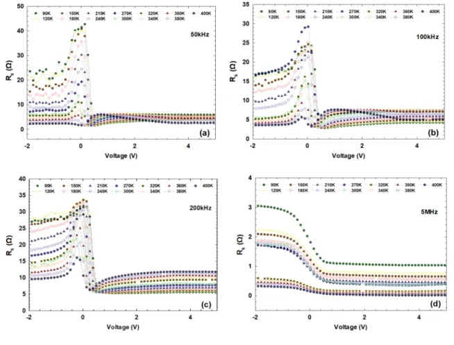
Moreover, The Rs–V–T curves, calculated using Eq. 13
and given in Fig. 4, are clearly dependent on both tempera-ture and voltage. These curves give peaks around 0 V for variable frequencies and shift towards the negative voltage regions as they increase with increasing temperature values. This is attributed to the reconstruction of the localized inter-face states Nss between GaAs-oxide and Eg under
tempera-ture [31, 34]. In Fig. 4a and b, the series resistance Rs values, which is corresponding to the high forward voltage regions, for MS structures were overlapped for all temperature lev-els, while they decreased with the increasing temperature in Fig. 4c and d. Thus, the values of Rs depend on both voltage and frequency magnitudes. In addition, these values are influenced by the regional Nss distributions between the
metal and the semiconductor.
Therefore, it is very important to obtain and analyze the Nss profile of the Re/n-GaAs or MS-based structures
prepared within the scope of the study. Nss is compensated
(13) RS= Gm G2 m+ 𝜔2Cm2 (14) Cox= Cm [ 1+ ( Gm 𝜔Cm )2]
Table 1 The basic electronic parameters obtained by C−2–V–T characteristics for Re/n-GaAs type MS structures
T (K) tanθ R2 V
bi (V) VD (V) Nc (cm−3) ND (cm−3) EF (eV) Em (V/cm) ФB (eV) ФB (eV) WD (cm) 50 kHz 90 1.287 × 10¹⁷ 0.931 0.690 0.697938 7.15× 10¹⁶ 2.67× 10¹⁵ 2.55× 10⁻² 2.27× 10⁴ 1.58× 10⁻² 0.71 6.15× 10⁻⁵ 120 1.578 × 10¹⁷ 0.928 0.650 0.660791 1.10× 10¹⁷ 2.18× 10¹⁵ 4.06× 10⁻² 1.99× 10⁴ 1.48× 10⁻² 0.69 6.63× 10⁻⁵ 150 1.722 × 10¹⁷ 0.920 0.604 0.616593 1.54× 10¹⁷ 1.99× 10¹⁵ 5.62× 10⁻² 1.84× 10⁴ 1.42× 10⁻² 0.66 6.69× 10⁻⁵ 180 2.223 × 10¹⁷ 0.934 0.547 0.562866 2.02× 10¹⁷ 1.55× 10¹⁵ 7.56× 10⁻² 1.55× 10⁴ 1.31× 10⁻² 0.63 7.26× 10⁻⁵ 210 1.509 × 10¹⁶ 0.896 0.531 0.549109 2.55× 10¹⁷ 2.23× 10¹⁵ 8.58× 10⁻² 1.84× 10⁴ 1.42× 10⁻² 0.62 5.97× 10⁻⁵ 240 2.858 × 10¹⁷ 0.941 0.450 0.471101 3.11× 10¹⁷ 1.20× 10¹⁵ 1.15× 10⁻¹ 1.25× 10⁴ 1.17× 10⁻² 0.57 7.53× 10⁻⁵ 270 1.225 × 10¹⁷ 0.922 0.450 0.473023 3.72× 10¹⁷ 2.80× 10¹⁵ 1.14× 10⁻¹ 1.91× 10⁴ 1.45× 10⁻² 0.57 4.94× 10⁻⁵ 300 1.517 × 10¹⁷ 0.936 0.388 0.414291 4.35× 10¹⁷ 2.26× 10¹⁵ 1.36× 10⁻¹ 1.61× 10⁴ 1.33× 10⁻² 0.54 5.15× 10⁻⁵ 320 1.379 × 10¹⁷ 0.928 0.358 0.38535 4.79× 10¹⁷ 2.49× 10¹⁵ 1.45× 10⁻¹ 1.63× 10⁴ 1.34× 10⁻² 0.52 4.73× 10⁻⁵ 340 2.008 × 10¹⁷ 0.928 0.298 0.327454 5.25× 10¹⁷ 1.71× 10¹⁵ 1.68× 10⁻¹ 1.24× 10⁴ 1.17× 10⁻² 0.48 5.26× 10⁻⁵ 360 9.774 × 10¹⁶ 0.929 0.303 0.33134 5.72× 10¹⁷ 3.51× 10¹⁵ 1.58× 10⁻¹ 1.79× 10⁴ 1.40× 10⁻² 0.48 3.69× 10⁻⁵ 380 7.084 × 10¹⁶ 0.934 0.273 0.305775 6.20× 10¹⁷ 4.85× 10¹⁵ 1.59× 10⁻¹ 2.02× 10⁴ 1.49× 10⁻² 0.45 3.02× 10⁻⁵ 400 2.507 × 10¹⁷ 0.963 0.137 0.171968 6.70× 10¹⁷ 1.37× 10¹⁵ 2.13× 10⁻¹ 8.07× 10⁴ 9.42× 10⁻³ 0.38 4.26× 10⁻⁵ 100 kHz 90 5.705× 10¹⁷ 0.992 0.687 0.694763 7.15× 10¹⁶ 6.02× 10¹⁴ 3.70× 10⁻² 1.08× 10⁴ 1.09× 10⁻² 0.72 1.29× 10⁻⁴ 120 5.801× 10¹⁷ 0.993 0.665 0.675119 1.10× 10¹⁷ 5.92× 10¹⁴ 5.40× 10⁻² 1.05× 10⁴ 1.07× 10⁻² 0.72 1.28× 10⁻⁴ 150 5.921× 10¹⁷ 0.988 0.631 0.643579 1.54× 10¹⁷ 5.80× 10¹⁴ 7.21× 10⁻² 1.02× 10⁴ 1.06× 10⁻² 0.71 1.27× 10⁻⁴ 180 5.921× 10¹⁷ 0.988 0.631 0.646164 2.02× 10¹⁷ 5.80× 10¹⁴ 9.08× 10⁻² 1.02× 10⁴ 1.06× 10⁻² 0.73 1.27× 10⁻⁴ 210 5.913× 10¹⁷ 0.986 0.549 0.566736 2.55× 10¹⁷ 5.81× 10¹⁴ 1.10× 10⁻¹ 9.54× 10³ 1.02× 10⁻² 0.67 1.19× 10⁻⁴ 240 5.317× 10¹⁷ 0.958 0.524 0.545166 3.11× 10¹⁷ 6.46× 10¹⁴ 1.28× 10⁻¹ 9.86× 10³ 1.04× 10⁻² 0.66 1.11× 10⁻⁴ 270 4.064× 10¹⁷ 0.976 0.509 0.532702 3.72× 10¹⁷ 8.45× 10¹⁴ 1.42× 10⁻¹ 1.12× 10⁴ 1.11× 10⁻² 0.66 9.55× 10⁻⁵ 300 5.840× 10¹⁷ 0.984 0.417 0.44252 4.35× 10¹⁷ 5.88× 10¹⁴ 1.71× 10⁻¹ 8.48× 10³ 9.65× 10⁻³ 0.60 1.04× 10⁻⁴ 320 5.938× 10¹⁷ 0.992 0.372 0.399865 4.79× 10¹⁷ 5.78× 10¹⁴ 1.85× 10⁻¹ 7.99× 10³ 9.37× 10⁻³ 0.58 1.00× 10⁻⁴ 340 5.654× 10¹⁷ 0.989 0.338 0.3677 5.25× 10¹⁷ 6.08× 10¹⁴ 1.98× 10⁻¹ 7.86× 10³ 9.29× 10⁻³ 0.56 9.36× 10⁻⁵ 360 5.218× 10¹⁷ 0.986 0.306 0.337101 5.72× 10¹⁷ 6.58× 10¹⁴ 2.10× 10⁻¹ 7.83× 10³ 9.28× 10⁻³ 0.54 8.61× 10⁻⁵ 380 4.574× 10¹⁷ 0.987 0.273 0.305925 6.20× 10¹⁷ 7.51× 10¹⁴ 2.20× 10⁻¹ 7.97× 10³ 9.36× 10⁻³ 0.52 7.68× 10⁻⁵ 400 3.814× 10¹⁷ 0.990 0.222 0.256507 6.70× 10¹⁷ 9.01× 10¹⁴ 2.28× 10⁻¹ 7.99× 10³ 9.37× 10⁻³ 0.48 6.42× 10⁻⁵ 200 kHz 90 3.495× 10¹⁷ 0.999 0.961 0.969118 7.15× 10¹⁶ 9.83× 10¹⁴ 3.32× 10⁻² 1.62× 10⁴ 1.34× 10⁻² 0.99 1.19× 10⁻⁴ 120 3.660× 10¹⁷ 0.993 0.918 0.92857 1.10× 10¹⁷ 9.39× 10¹⁴ 4.93× 10⁻² 1.55× 10⁴ 1.31× 10⁻² 0.96 1.20× 10⁻⁴ 150 4.132× 10¹⁷ 0.999 0.829 0.84163 1.54× 10¹⁷ 8.31× 10¹⁴ 6.75× 10⁻² 1.39× 10⁴ 1.24× 10⁻² 0.90 1.21× 10⁻⁴ 180 4.349× 10¹⁷ 0.997 0.771 0.786358 2.02× 10¹⁷ 7.90× 10¹⁴ 8.60× 10⁻² 1.31× 10⁴ 1.20× 10⁻² 0.86 1.20× 10⁻⁴ 210 4.264× 10¹⁷ 0.987 0.722 0.74056 2.55× 10¹⁷ 8.06× 10¹⁴ 1.04× 10⁻¹ 1.28× 10⁴ 1.19× 10⁻² 0.83 1.15× 10⁻⁴ 240 4.394× 10¹⁷ 0.985 0.662 0.682235 3.11× 10¹⁷ 7.82× 10¹⁴ 1.24× 10⁻¹ 1.21× 10⁴ 1.16× 10⁻² 0.79 1.12× 10⁻⁴ 270 4.869× 10¹⁷ 0.997 0.622 0.644875 3.72× 10¹⁷ 7.06× 10¹⁴ 1.46× 10⁻¹ 1.12× 10⁴ 1.11× 10⁻² 0.78 1.15× 10⁻⁴ 300 4.567× 10¹⁷ 0.990 0.553 0.579021 4.35× 10¹⁷ 7.52× 10¹⁴ 1.64× 10⁻¹ 1.10× 10⁴ 1.10× 10⁻² 0.73 1.06× 10⁻⁴ 320 4.440× 10¹⁷ 0.990 0.517 0.544742 4.79× 10¹⁷ 7.74× 10¹⁴ 1.77× 10⁻¹ 1.08× 10⁴ 1.09× 10⁻² 0.71 1.01× 10⁻⁴ 340 4.495× 10¹⁷ 0.993 0.471 0.500507 5.25× 10¹⁷ 7.64× 10¹⁴ 1.91× 10⁻¹ 1.03× 10⁴ 1.06× 10⁻² 0.68 9.74× 10⁻⁵ 360 4.337× 10¹⁷ 0.992 0.439 0.469736 5.72× 10¹⁷ 7.92× 10¹⁴ 2.04× 10⁻¹ 1.01× 10⁴ 1.06× 10⁻² 0.66 9.27× 10⁻⁵ 380 4.158× 10¹⁷ 0.997 0.402 0.434373 6.20× 10¹⁷ 8.26× 10¹⁴ 2.17× 10⁻¹ 9.96× 10³ 1.05× 10⁻² 0.64 8.72× 10⁻⁵ 400 3.590× 10¹⁷ 0.995 0.369 0.403269 6.70× 10¹⁷ 9.57× 10¹⁴ 2.26× 10⁻¹ 1.03× 10⁴ 1.07× 10⁻² 0.62 7.81× 10⁻⁵ 5 MHz 90 1.296× 10¹⁶ 0.996 1.094 1.10146 7.15× 10¹⁶ 2.65× 10¹⁶ 7.70× 10⁻³ 8.98× 10⁴ 3.14× 10⁻² 1.08 2.45× 10⁻⁵ 120 1.146× 10¹⁶ 0.991 1.111 1.12105 1.10× 10¹⁷ 3.00× 10¹⁶ 1.35× 10⁻² 9.63× 10⁴ 3.25× 10⁻² 1.10 2.33× 10⁻⁵ 150 1.203× 10¹⁶ 0.994 0.975 0.987454 1.54× 10¹⁷ 2.86× 10¹⁶ 2.18× 10⁻² 8.83× 10⁴ 3.11× 10⁻² 0.98 2.24× 10⁻⁵ 180 1.135× 10¹⁶ 0.988 0.907 0.9224 2.02× 10¹⁷ 3.03× 10¹⁶ 2.95× 10⁻² 8.78× 10⁴ 3.11× 10⁻² 0.92 2.10× 10⁻⁵ 210 1.013× 10¹⁶ 0.990 0.866 0.883659 2.55× 10¹⁷ 3.39× 10¹⁶ 3.65× 10⁻² 9.10× 10⁴ 3.16× 10⁻² 0.89 1.94× 10⁻⁵ 240 1.001× 10¹⁶ 0.978 0.819 0.840006 3.11× 10¹⁷ 3.43× 10¹⁶ 4.56× 10⁻² 8.92× 10⁴ 3.13× 10⁻² 0.85 1.88× 10⁻⁵ 270 8.476× 10¹⁵ 0.996 0.864 0.887037 3.72× 10¹⁷ 4.05× 10¹⁶ 5.16× 10⁻² 9.97× 10⁴ 3.31× 10⁻² 0.91 1.78× 10⁻⁵
by metal side if the thickness of the native oxide layer is
δox < 30 Ǻ, and by semiconductor if it is δox≥ 30 Ǻ, as a
result of charge transitions. In the study, Nss states are in equilibrium with the semiconductor.
C–V measurements for MS structure applications are
carried out utilizing an applied AC voltage signal (dVac)
and a DC voltage (Vdc), as shown in Fig. 5a [35]. For AC voltage signal, while Nss can easily follow the AC signal
at low frequencies (f ≤ 100 Hz), it can hardly follow at high frequencies (f ≥ 1 MHz). Because the period of the AC signal is T = 1∕2𝜋f and τ in the trap are smaller than the lifetime of the charges. Therefore, the Nss profile in the
study was calculated using the combined high (CHF)–low
(CLF) frequency capacitance method expressed as below
[15], although there are many methods available in the literature for MS-based structures [16, 36, 37].
Also, the Nss values obtain from this equation were given in Fig. 5b. As it can be seen, Nss–V–T curves give peaks in the range of − 0.1 V to 0.7 V at variable temperatures and the Nss values decrease with increasing temperature and shift
towards negative bias regions.
(15) Nss= 1 qA [ ( 1 CLF − 1 Cox )−1 − ( 1 CHF − 1 Cox )−1] Table 1 (continued) T (K) tanθ R2 V
bi (V) VD (V) Nc (cm−3) ND (cm−3) EF (eV) Em (V/cm) ФB (eV) ФB (eV) WD (cm) 300 7.835× 10¹⁵ 0.996 0.862 0.887629 4.35× 10¹⁷ 4.38× 10¹⁶ 5.93× 10⁻² 1.04× 10⁵ 3.38× 10⁻² 0.91 1.71× 10⁻⁵ 320 7.207× 10¹⁵ 0.996 0.869 0.891473 4.79× 10¹⁷ 4.77× 10¹⁶ 6.37× 10⁻² 1.08× 10⁵ 3.45× 10⁻² 0.92 1.65× 10⁻⁵ 340 6.924× 10¹⁵ 0.994 0.786 0.815394 5.25× 10¹⁷ 4.96× 10¹⁶ 6.91× 10⁻² 1.06× 10⁵ 3.41× 10⁻² 0.85 1.54× 10⁻⁵ 360 6.359× 10¹⁵ 0.994 0.768 0.799071 5.72× 10¹⁷ 4.96× 10¹⁶ 7.32× 10⁻² 1.09× 10⁵ 3.46× 10⁻² 0.84 1.46× 10⁻⁵ 380 5.879× 10¹⁵ 0.998 0.727 0.75935 6.20× 10¹⁷ 5.84× 10¹⁶ 7.74× 10⁻² 1.11× 10⁵ 3.49× 10⁻² 0.80 1.37× 10⁻⁵ 400 4.732× 10¹⁵ 0.996 0.718 0.75258 6.70× 10¹⁷ 7.26× 10¹⁶ 7.66× 10⁻² 1.23× 10⁵ 3.67× 10⁻² 0.79 1.23× 10⁻⁵
Fig. 4 Rs–V–T curves of MS structures at variable frequencies
Fig. 5 To analyze the Nss profile of the MS structures: a AC and DC voltage signals of C–V sweep measurement, b Nss–V curves at variable temperatures
In addition, the highest Nss values were obtained as 1.04 × 10¹⁴, 5.59 × 10¹³, and 9.89 × 10¹³ eV−1 cm−2 for 300,
340, and 400 K temperatures, respectively. Here, it can be concluded that under variable temperatures, the charges on the interface with e−–h+ pairs are rearranged and configured.
4 Conclusion
Experimentally, Re/n-GaAs with a native oxide layer based on MS structures were fabricated to investigate their prop-erties according to similar structures. In addition, the elec-tronic parameters for instance Vbi, EF, ФB, WD, Rs, Nss etc.
using the developed LabVIEW-based program was calcu-lated from raw data of C–V–T and G/ω–V–T measurements in the frequency range from 50 kHz to 5 MHz. The effects of
Rs, Nss and the oxide layer between Re and GaAs were
inves-tigated under different temperature and frequency. It is deter-mined that the increased C values, especially in the deple-tion and strong accumuladeple-tion regions, depend significantly on the temperature at variable frequencies due to the pres-ence of the Rs and the Nss in the forbidden energy gap and a
native oxide layer between M and S. Moreover, these values exhibit an increasing behavior, especially with a decreasing frequency in the depletion regions, owing to the presence of
Nss. G/ω values, which decreased with increasing frequency in forward and reverse bias regions, are quite dependent on temperature, like the obtained C–V–T curves. This behavior was attributed to the presence of the Rs. On the other hand,
as can be seen below from the characteristics of the C–V–T, the C values exhibit an increasing behavior, especially with a decreasing frequency in the depletion regions, and these curves give a peak at about 0.5 V. In the strong accumula-tion regions (VG ≫ 0), the decrease in C–V–T curves at
vari-able frequencies attributes the presence of series resistance (Rs). Both the magnitudes of temperature and voltage affect
significantly the obtained Rs values, which give peak 0 V
for variable frequencies and shift towards negative voltage regions with the increasing temperatures, due to the recon-struction of the localized interface states Nss between
GaAs-oxide and Eg. It can be concluded that, the Nss values give
peaks in the range of − 0.1 V to 0.7 V and shift towards negative bias regions with increasing temperature, because the charges on the interface with e−–h+ pairs are rearranged
and configured under variable temperatures.
References
1. E.H. Rhoderick, Metal-Semiconductor Contacts (Oxford Univer-sity Press, Oxford, 1978)
2. K. Kano, Semiconductor Devices (Prentice-Hall, Upper Saddle River, 1998)
3. B. Sharma, Metal-Semiconductor Schottky Barrier Junctions and
Their Applications (Plenum Press, New York, 1984)
4. S.O. Tan, H. Tecimer, O. Çiçek, Comparative investigation on the effects of organic and inorganic interlayers in Au/n-GaAs Schottky diodes. IEEE Trans. Electron Dev. 64(3), 984–990 (2017) 5. H. Yang, J. Gao, H. Nakashima, Investigation of ZrGe Schottky
source/drain contactsfor Ge p-channel MOSFETs. Mater. Sci. Semicond. Process. 26, 614–619 (2014)
6. D.B. Patel, K.R. Chauhan, S.-H. Park, J. Kim, High-performing transparent photodetectors based on Schottky contacts. Mater. Sci. Semicond. Process. 64, 137–142 (2017)
7. A.M. Cowley, S.M. Sze, Surface states and barrier height of metal-semiconductor system. J. Appl. Phys. 36(10), 3212 (1965) 8. S.-W. Kim, S.-H. Kim, G.-S. Kim, C. Choi, R. Choi, H.-Y. Yu,
The Effect of interfacial dipoles on the metal-double interlayers-semiconductor structure and their application in contact resistivity reduction. ACS Appl. Mater. Interfaces. 8, 35614–35620 (2016) 9. Ç. Güçlü, A. Özdemir, A. Karabulut, A. Kökce, Ş. Altındal, Inves-tigation of temperature dependent negative capacitance in the for-wardbias C–V characteristics of (Au/Ti)/Al2O3/n-GaAs Schottky barrier diodes (SBDs). Mater. Sci. Semicond. Process. 89, 26–31 (2019)
10. O. Çiçek, S. Kurnaz, A. Bekar, Ö. Öztürk, Comparative investiga-tion on electronic properties of metal-semiconductor structures with variable ZnO thin film thickness for sensor applications. Composites B 174, 106987 (2019)
11. S. Tan, H. Uslu Tecimer, O. Çiçek, H. Tecimer, İ. Orak, Ş. Altındal, Electrical characterizations of Au/ZnO/n-GaAs Schottky diodes under distinct illumination intensities. J. Mater. Sci.: Mater. Electron. 27(8), 8340–8347 (2017)
12. H. Durmuş, H.Ş. Kılıç, S.Y. Gezgin, Ş. Karataş, Analysis of cur-rent–voltage–temperature and capacitance–voltage–temperature characteristics of Re/n-Si Schottky contacts. Silicon 10, 361–369 (2018)
13. A. Buyukbas-Ulusan, I. Taşçıoğlu, A. Tataroğlu, F. Yakuphanoğlu, S. Altındal, A comparative study on the electrical and dielectric properties of Al/Cd-doped ZnO/p-Si structures. J. Mater. Sci.: Mater. Electron. 30(13), 12122–12129 (2019)
14. E. Erbilen Tanrıkulu, Ş. Altındal, Y. Azizian-Kalandaragh, Preparation of (CuS–PVA) interlayer and the investigation their structural, morphological and optical properties and frequency dependent electrical characteristics of Au/(CuS–PVA)/n-Si (MPS) structures. J. Mater. Sci.: Mater. Electron. 29(14), 11801–11811 (2018)
15. E. Nicollian, J. Brews, MOS(Metal Oxide Semiconductor
Phys-ics and Technology) (Bell Telephone Laboratories, Incorporated,
Canada, 1982)
16. E. Nicollian, A. Goetzberger, The Si–SiO2 interface-electrical properties as determined by the metal-insulator-silicon conduct-ance technique. Bell Syst. Technol. J. 46(6), 1055–1133 (1967) 17. I. Taşçıoğlu, S. Tan, Ş. Altındal, Frequency, voltage and
illumina-tion interacillumina-tion with the electrical characteristics of the CdZnO interlayered Schottky structure. J. Mater. Sci.: Mater. Electron.
30(12), 11536–11541 (2019)
18. S. Altındal, Ö. Sevgili, Y. Azizian-Kalandaragh, The structural and electrical properties of the Au/n-Si (MS) diodes with nano-composites interlayer (Ag-doped ZnO/PVP) by using the simple ultrasound-assisted method. IEEE Trans. Electron Dev. 66(7), 3103–3109 (2019)
19. D. Korucu, Ş. Altindal, T.S. Mammadov, S. Özçelik, Origin of anomalous peak and negative capacitance in the forward bias
C–V characteristics of Au/n-InP Schottky barier diodes (SBDs).
20. H. Durmuş, M. Yıldırım, Ş. Altındal, On the possible conduc-tion mechanisms in Rhenium/n–GaAs Schottky barrier diodes fabricated by pulsed laser deposition in temperature range of 60–400 K. J. Mater. Sci.: Mater. Electron. (2019). https ://doi. org/10.1007/s1085 4-019-01233 -z
21. O. Çiçek, S. Kurnaz, LabVIEW based a software system: quan-titative determination of main electronic parameters for Schottky junction structures. Balk. J. Electr. Comput. Eng. 7(3), 326–331 (2019)
22. D. Sands, K. Brunson, M. Tayarani-Najaran, Measured intrinsic defect density throughout the entire band gap at the 〈100〉 Si/SiO2 interface. Semicond. Sci. Technol. 7(8), 1091–1096 (1992) 23. P. Ho, E. Yang, H. Evans, X. Wu, Phys. Rev. Lett. 60, 177–180
(1986)
24. Ş. Altındal, H. Uslu, J. Appl. Phys. 109, 074503 (2011) 25. J. Werner, A.F.J. Levi, R.T. Tung, M. Anzlowar, M. Pinto, Phys.
Rev. Lett. 60, 53–56 (1988)
26. X. Wu, E.S. Yang, J. Appl. Phys. 65, 3560 (1989)
27. P. Chattopadhyay, B. Raychaudhuri, Solid State Electron. 35, 875 (1992)
28. M. Ershov, H.C. Liu, L. Li, M. Buchanan, Z.R. Wasilewski, A.K. Jonscher, IEEE Trans. Electron. Dev. 45, 2196–2206 (1998) 29. E. Arslan, Y. Şafak, Ş. Altındal, Ö. Kelekçi, E. Özbay, Non-Cryst.
Solids 356, 1006–1011 (2010)
30. D. Korucu, A. Turut, S. Altındal, Curr. Appl. Phys. 13(6), 1101– 1108 (2013)
31. S. Sze, K.K. Ng, Physics of Semiconductor Devices, 3rd edn. (Wiley, New Jersey, 2007)
32. A. Sing, K. Reinhart, W. Anderson, Temperature dependence of the electrical characteristics of Yb/p-InP tunnel metal-insulator-semiconductor junctions. J. Appl. Phys. 68(7), 3475–3484 (1990) 33. P. Chattopadhyay, B. Raychaudhuri, Frequency dependence of
forward capacitance–voltage characteristics of Schottky barrier diodes. Solid-State Electron 36(4), 605–610 (1993)
34. H. Card, E. Rhoderick, Studies of tunnel MOS diodes I. Inter-face effects in silicon Schottky diodes. J. Phys. D Appl. Phys. 4, 1589–1601 (1971)
35. Keithley, C–V Characterization of MOS Capacitors Using
the Model 4200-SCS Semiconductor Characterization System
(Keithley Instruments, Inc., Cleveland, 2007)
36. R. Castange, A. Vapaille, Description of the SiO2–Si interface properties by means of very low frequency MOS capacitance. Surf. Sci. 28, 157–193 (1971)
37. K. Kwa, S. Chattopadhyay, N. Jankovic, S. Olsen, L. Driscoll, A. O’Neill, A model for capacitance reconstruction from measured lossy MOS capacitance–voltage characteristics. Semicond. Sci. Technol. 18, 82–87 (2003)
Publisher’s Note Springer Nature remains neutral with regard to jurisdictional claims in published maps and institutional affiliations.