Sami Pekdemir, Ilker Torun, Menekse Sakir, Mahmut Ruzi, John A. Rogers,
*
and M. Serdar Onses
*
Cite This:ACS Nano 2020, 14, 8276−8286 Read Online
ACCESS
Metrics & More Article Recommendations*
sı Supporting InformationABSTRACT: Spatially defined assembly of colloidal metallic nanoparticles is necessary for fabrication of plasmonic devices. In this study, we demonstrate high-resolution additive jet printing of end-functional polymers to serve as templates for directed self-assembly of nanoparticles into architectures with substantial plasmonic activity. The intriguing aspect of this work is the ability to form patterns of end-grafted poly(ethylene glycol) through printing on a hydrophobic layer that consists of fluoroalkylsilanes. The simultaneous dewetting of the under-lying hydrophobic layer together with grafting of the printed polymer during thermal annealing enables fabrication of spatially defined binding sites for assembly of nanoparticles. The employment of electrohydrodynamic jet printing and
aqueous inks together with reduction of the feature size during thermal annealing are critically important in achieving high chemical contrast patterns as small as∼250 nm. Gold nanospheres of varying diameters selectively bind and assemble into nanostructures with reduced interparticle distances on the hydrophilic patterns of poly(ethylene glycol) surrounded with a hydrophobic background. The resulting plasmonic arrays exhibit intense and pattern-specific signals in surface-enhanced Raman scattering (SERS) spectroscopy. The localized seed-mediated growth of metallic nanostructures over the patterned gold nanospheres presents further routes for expanding the composition of the plasmonic arrays. A representative application in SERS-based surface encoding is demonstrated through large-area patterning of plasmonic structures and multiplex deposition of taggant molecules, all enabled by printing.
KEYWORDS: colloidal nanoparticles, plasmonics, self-assembly, printing, surface-enhanced Raman scattering, polymers
C
olloidal metallic nanoparticles provide important molecular engineering pathways for a set of technologically critical applications in sensing,1 renew-able energy,2 authentication,3 catalysis,4 and metamaterials.5 These and other applications require assembly of colloidal building blocks into spatially defined architectures. At the core of this requirement is to couple individual plasmons of nanoparticles in a way to enhance and tailor their collective properties.6 Reducing the interparticle distances of metallic nanoparticles, for example, allows for focusing of light into plasmonic hot spots, which consist of locally enhanced electromagnetic fields.7,8 These hot spots are of significant interest for sensing and other applications, since they can significantly increase scattering of light and fluorescence.9Surface-enhanced Raman scattering (SERS), in particular, is a powerful approach for obtaining molecular information at extremely low concentrations.10−13 In addition to capabilities in sensing, SERS provides advanced routes for preparation of
encoded surfaces that may be used to protect products against counterfeiting.14For SERS and other applications, there is an urgent need for assembling colloidal metallic nanoparticles into spatially defined arrays with high plasmonic activity.
Patterning of colloids into spatially defined assemblies has been a topic of immense interest. Lithography techniques provide precise control over the size and geometry of the patterns at a perfection inherited from the semiconductor industry. Topographic patterns can trap the nanoparticles by capillary15 and electrophoretic16 forces, whereas chemical
Received: March 6, 2020
Accepted: June 22, 2020
Published: June 22, 2020
Downloaded via BILKENT UNIV on February 12, 2021 at 11:14:13 (UTC).
binding sites17can selectively adsorb these nanoscale building blocks. Other than transformation of resist patterns into topographic and chemical templates, colloidal nanomaterials can be engineered to serve as resists in photolithography18and electron beam19lithography systems. The need for cleanroom infrastructure and multistep, mostly subtractive, processes together with challenges in terms of the planarity of the substrate has motivated researchers for other patterning approaches. Self-assembly of block copolymers20 and DNA nanostructures21 present interesting opportunities, with the lack of long-range order. Scanning probe-based lithography approaches together with nanoscale confinement of block copolymer inks provide ways for in situ synthesis of single nanoparticle arrays of small nanoparticles.22SERS and some other plasmonic applications require close placement of multiple nanoscale building blocks with different geometries
and sizes that are typically larger than 20 nm. Soft lithography23 is yet another attractive route from direct printing of nanoparticles to generation of binding sites for assembly of colloids.24−26Despite the quiet flexible nature of this approach, the need for masters is a barrier toward rapid prototyping of desired structure. Room-temperature on-demand inkjet printing offers a cost-effective, additive path for rapid assembly of colloidal nanomaterials.27,28The smallest feature sizes on the order of 10 μm is a limiting factor for fabricating spatially defined assemblies of colloidal nanoma-terials using piezoelectric inkjet printers.
Electrohydrodynamic jet (e-jet) printing is an additive technology capable of direct patterning of a range of different materials with nanoscale resolution. In e-jet printing, droplets of desired materials are ejected from the metal-coated tip of a nozzle by applying a voltage between the nozzle and
Figure 1. Self-assembly of plasmonic arrays enabled by chemical funneling of colloidal gold NSs on patterns of end-grafted PEG layers printed on the hydrophobic substrate. (a) Schematic illustration of the modification of the substrate with a layer of FAS. The cleaned silicon substrate was coated with a layer of FAS, which makes the substrate hydrophobic (CA = 105°). It should be emphasized that not all surface silanol groups are consumed by FAS, as depicted in the schematic. (b) An aqueous PEG solution is e-jet printed on the hydrophobic substrate, followed by annealing and washing, which results in end-grafted polymer layers. The drop-casting of colloidal gold NSs followed by washing results in plasmonic arrays. (c) Optical microscope image of a large-area array of printed dots. (d) AFM image of an array of end-grafted PEG layers following printing, annealing, and washing on the hydrophobic substrate. (e) Large-area view SEM image of an array of gold NSs. (f) SEM images of gold NSs assembled on PEG patterns of varying size. The assembly of gold NSs was performed by sequential deposition of the particles with a diameter of 60 and 20 nm, each for 1 h.
substrate.29−31 The ease-of usage, cost-effectiveness, and versatility of the technique have galvanized scientists and engineers, who have employed the technique to fabricate patterned quantum dots,32perovskite nanocrystals,33 metallic nanostructures,34and biomolecules.35,36Important advantages of e-jet printing over other nanofabrication approaches37−39 include room-temperature additive operation and access to nonperiodic geometries. In comparison with other types of inkjet printing techniques, e-jet printers offer higher levels of resolution31that can approach a length scale on the order of the size of plasmonic nanoparticles. Additionally, e-jet printing offers the possibility of processing inks with a broad range of viscosities, allowing for patterning materials in different forms, such as nanofibers40 and three-dimensional structures.41 A practical difficulty for fabricating plasmonic arrays using colloidal inks involves the use of particle-containing inks that can easily clog the fine nozzles. Even in the case of conventional piezoelectric printers, it is challenging to formulate inks for colloidal nanoparticles of varying size and geometry. This challenge becomes more significant in printing of plasmonic nanoparticles with relatively large diameters (e.g., >20 nm) into close proximity to facilitate formation of plasmonic hot spots. The use of dilute inks and large nozzles precludes fabrication of plasmonic hot spots and patterns with small critical dimensions, respectively.
In the following, we present a chemical patterning approach using e-jet printing for assembling colloidal gold nanoparticles into plasmonic arrays. The essential advantages of this approach are the use of particle-free inks and the ability to assemble colloidal plasmonic nanoparticles into hot spot containing architectures. For this purpose, we engineer aqueous inks that are composed of poly(ethylene glycol) (PEG). The inherent hydroxyl groups that are present at the ends of the polymer provide versatile grafting on the silicon oxide terminated surfaces through a swift heat treatment. A challenge in e-jet printing assisted patterning of PEG is significant spreading of the hydrophilic polymer during thermal annealing, resulting in patterns with dimensions significantly larger than the printed ones and reducing the chemical contrast, both of which are critical for selective assembly of nanoparticles into plasmonically active architectures. To circumvent these challenges, we modify the surface of the substrate through chemical vapor deposition using a hydro-phobic layer that consists of a polysiloxane composed of
fluoroalkylsilane (FAS). The intriguing ability of PEG chains to tunnel through the existing hydrophobic layer during thermal annealing enables fabrication of high-resolution and chemical contrast patterns of end-grafted polymers at grafting densities significantly higher than homogeneous substrates. The hydro-phobic background also enables effective funneling of colloidal gold nanoparticles into the patterns at binding densities that are substantially higher than the unpatterned and printed patterns on the bare hydrophilic substrates. The selective assembly of colloidal gold nanoparticles of different diameters into patterned plasmonic architectures enables region-specific and significantly high SERS intensities.
RESULTS AND DISCUSSION
Figure 1presents the key steps and results on fabrication of printed patterns composed of end-grafted PEG layers for guided assembly of colloidal gold nanospheres (NSs). First, a Si substrate is cleaned and UV-ozone treated to increase the number of silanol groups (−Si−OH) on the surface, resulting in a hydrophilic surface with a water contact angle of <10°. The hydrophobic derivatization is achieved by vapor-phase deposition of FAS onto the hydrophilic silicon substrate.42For the surface modification, we used tridecafluoro-1,1,2,2-tetrahydrooctyltrichlorosilane, whichfirst goes through hydrol-ysis reaction with residual water on the substrate and in air, followed by condensation reaction with the surface silanol groups. Vapor-phase deposition in an air environment is critically important in depositing a hydrophobic layer consisting of self-polymerized oligomers, which do not block all silanol groups on the surface of the substrate (Figure 1a). Depending on the vapor-phase deposition time, initially afilm of FAS with a thickness up to 20 nm is deposited on the substrate (seeSupporting Information Figure S1 for details). The removal of excess material by repeated washing under sonication in water and ethanol reduces thefilm thickness to a couple of nanometers, implying the removal of unreacted FAS layers (Figure S1). Despite the reduced film thickness, the deposition of FAS imparts hydrophobicity with a water contact angle of 105°. An aqueous ink of PEG is then directly e-jet printed on the modified substrate (Figure 1b). This ink formulation allows for printing PEG over large surfaces areas (Figure 1c). A brief (i.e., 5 min at 120°C) thermal annealing allows for swift grafting of the PEG chains via the condensation reaction between the end hydroxyl groups and surface silanols
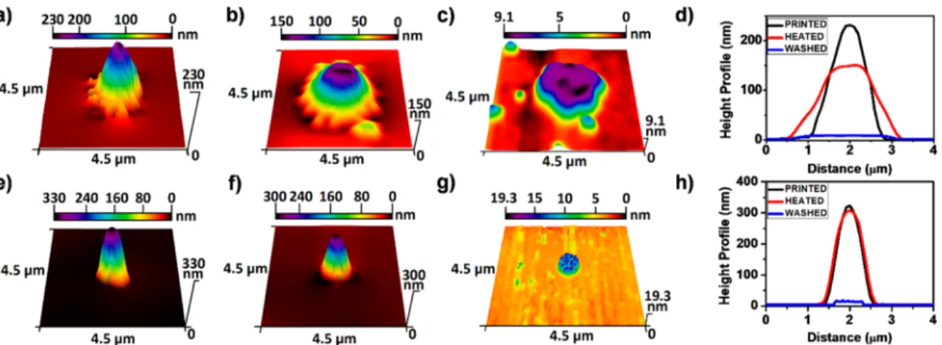
Figure 2. AFM analysis of the grafting process on the hydrophilic and hydrophobic substrates. AFM images of a single printed PEG feature after (a, e) printing, (b, f) annealing, and (c, g) washing steps on the hydrophilic (top row) and hydrophobic (bottom row) substrates. The cross-sectional height profiles for (d) bare hydrophilic and (h) hydrophobic substrates.
that are present under the hydrophobic FAS layer. The excess and unreacted PEG is washed away through sonication in water. This washing results in patterned features with a height that approaches to 20 nm (Figure 1d; see Supporting Information Figure S2 for additional AFM images) with a diameter that depends on the size of the printed spots. The self-assembly of plasmonic structures is achieved by drop-casting colloidal gold NSs on the patterned substrate surface, followed by washing off unbounded and excess particles. This approach allows for preparation of plasmonic arrays as demonstrated by assembly of gold NSs (Figure 1e). The assembly can be confined into areas defined at the printing step with a size as small as 250 nm (Figure 1f). In all cases, gold NSs can be assembled at high densities with low levels of binding to the surrounding regions.
The wetting property of the substrate has a clear effect on spreading and broadening of the size of PEG spots during printing, annealing, and washing steps.Figure 2presents AFM images and cross-sectional height profiles of a printed PEG feature on the bare and hydrophobic substrate. On the bare hydrophilic surface (Figure 2top row), printed droplets have a base diameter of 1.7μm (Figure 2a), which extends to 2.5μm (Figure 2b) after annealing at 120 °C, while the height decreases to 150 nm from the initial height of 230 nm (Figure 2d). Thus, the necessary step of annealing to graft PEG onto the substrate leads to the unwanted effect of significant spreading. The diameter of the printed feature increases by 47% at an annealing temperature of 120 °C. Note that this spreading on the unmodified substrate greatly exceeds those30 for random copolymers of methyl methacrylate and styrene grafted at a temperature of 220°C. The high mobility of PEG chains (Tg< 0°C) together with affinity to the polar substrate
likely drives such a spreading at a reduced grafting temperature of 120°C and duration of 5 min. On the hydrophobic surface (Figure 2 bottom row), printed PEG features have the same base diameter as the inner diameter of the capillary needle (∼1 μm) used in the printing. The first effect of the hydrophobicity of the substrate is reduction in the size of printed patterns in comparison to the bare substrate. A striking contrast appears following thermal annealing, on the hydrophobic substrate, there is no spreading, and both the height and width of the printed features do not change significantly (Figure 2, Table 1). After washing off excess and weakly bounded PEGs, the
base diameters of the grafted PEG features decrease to 2.3μm and ∼700 nm on the bare and hydrophobic surfaces, respectively (Figure 2d and h). Overall, the grafted PEG feature size on the hydrophobic surface is almost three times smaller than on the hydrophilic surface, thus demonstrating the capabilities of surface modification coupled with e-jet printing for the fabrication of highly resolved submicroscopic patterns. The molecular weight and grafting density of the polymer determine the height of the patterns following removal of unreacted materials. The height of the patterned PEG layers was significantly higher on the hydrophobic substrate in
comparison with the hydrophilic substrate. The height of PEG features after washing and drying was 9.1 and 19.3 nm on the hydrophilic and hydrophobic substrates, respectively. The calculation (see Supporting Information for details) of the grafting density of the patterned PEG layers from these height values results in 0.17 chain/nm2 on the hydrophilic substrate
and 0.36 chain/nm2 on the hydrophobic substrate. The increased height and grafting density of the patterned PEG layers on the hydrophobic substrate can be attributed to higher levels of repulsion between polymer chains and strong osmotic pressure within the patterned feature, leading to extremely stretched PEG chains. The quantitative argument further confirms these observations and indicates that the polymers are in the brush regime. For a grafting density of 0.36 chain/nm2, the distance between grafting sites is 1.88 nm, which is smaller than twice the radius of gyration of PEG (Rg = 6.9 nm),
confirming that end-grafted PEG layers are in the brush regime.43Note that the grafting density of ∼0.36 chain/nm2
and height of 19.3 nm are significantly high when compared with previously reported homogeneous PEG layers44prepared by spin-coating of similar materials.
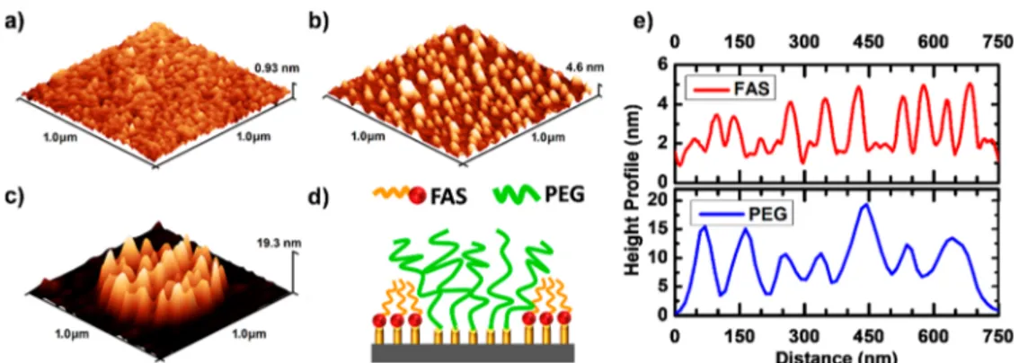
The grafted PEG patterns on the hydrophobic substrate exhibit a particular topography, distinctively different from patterned PEG layers grafted on the hydrophilic surface (Figure 3). This difference can be explained by examining the surface modification due to FAS deposition. The roughness of the deposited FAS film shows a noticeable increase with thermal annealing (Figure 3a,b). This texture is the result of formation and growth of FAS islands during the annealing process, as observed in previous studies.45−47The oligomers of FAS likely dewet during the thermal annealing process. The implication here is that there are unreacted Si−OH groups between mounds of FAS molecules that are available for PEGs to react with (see schematics in Figure 3d and Figure S3). Thus, on the hydrophobic surface, the PEG molecules react with available silanol groups of the silicon substrate and form PEG bundles between the FAS islands. The comparison of height profile of patterned PEG layers with that of unpatterned sample (silicon substrate treated with FAS) clearly supports the aforementioned mechanism (Figure 3e). Here, PEG chains form bundles with a maximum height of 19.3 nm intervened by 4.6 nm tall mounds (Figure 3e). To further understand the origin of this texture, we investigated the effect of the annealing temperature on the morphology of the FAS and end-grafted PEG layer. Figure S4 presents AFM images of the FAS deposited substrate following annealing at temperatures of 80 and 100°C. The topography becomes significant at 120 °C (Figure 3b), suggesting that lower temperatures are not sufficient to induce dewetting of FAS oligomers. Within the same range of grafting temperatures, the height of the end-grafted PEG patterns exhibited a significant reduction with decreasing grafting temperature (Figure S5). The grafting is likely to be hampered at low temperatures due to the diminished ability of PEG chains to reach and react with the silanol groups of the underlying substrate. The mobility of PEG chains, kinetics of the grafting reaction, and dewetting of FAS oligomers to reveal grafting sites should all depend on the temperature and contribute to these observations.
The ability to fabricate printed patterns of end-grafted PEG layers surrounded by a hydrophobic layer enables assembly of colloidal gold NSs into clusters with close interparticle distances resulting in high SERS activity. Shown inFigure 4
are Raman mapping images of a probe molecule, rhodamine Table 1. Height and Width of the Patterns
after printing after annealing after washing substrate height (nm) width (μm) height (nm) width (μm) height (nm) width (μm) hydrophilic 231.3 1.802 150.6 2.723 9.1 2.354 hydrophobic 323.2 1.164 307.3 1.313 19.3 0.700
6G (R6G), on arrays of gold NSs assembled on the patterns of PEG on the hydrophilic and hydrophobic substrates. To better see the impact of the hydrophobicity of the substrate, the assembly of gold NSs was performed by sequential deposition of particles with a diameter of 60 and 20 nm, respectively. The small particles bind at high densities andfill in the interstitial regions left from the large particles, ensuring effective visualization of the patterns. In the case of hydrophobic substrates, the inelastic scattering of light is greatly enhanced in the patterned regions, as demonstrated by the strong contrast in the SERS intensity. The boundary of the patterns becomes ambiguous with a reduction in the intensity on the bare hydrophilic substrates. The examination of SEM images presented in Figure 4b,d clearly establishes that the Raman mapping relates to the assembly behavior of gold NSs on the printed arrays of end-grafted PEG layers on the hydrophilic and hydrophobic substrates. On the hydrophobic surface, the patterned PEG features are small (Figure 4d) and there is a strong contrast between the background, whereas on the hydrophilic surface the features are large (Figure 4b) with ambiguous boundaries. SEM imaging clearly visualizes the difference in the assembly of colloidal gold NSs on the patterns. On the FAS deposited substrate, gold NSs assembled at high densities with a clear and sharp boundary that separates the patterns from the surrounding regions. The Raman spectra
shown inFigure 4e reveal that the SERS intensity of the probe molecule on the hydrophobic substrate is two times stronger than the one on the hydrophilic substrate, which is itself stronger than the SERS signal on the unpatterned surface. This result clearly shows the impact of the background wetting properties for the assembly of colloidal gold nanoparticles and their SERS activity.
The assembly and SERS response of the gold NSs are cooperatively determined by the substrate wetting property and grafting profile of PEG chains within the patterns. The improved SERS activity of the plasmonic arrays prepared on the hydrophobic substrate in comparison with the hydrophilic substrate is likely a consequence of the close placement of the gold NSs favoring formation of plasmonic hot spots.48 We think that multiple interrelated factors contribute to this observation. First, the height of end-grafted PEG layers is significantly high on the hydrophobic substrate, allowing for more polymer chains to interact with the gold NSs. To further verify this behavior, gold NSs were assembled on patterns of PEG that were end-grafted at varying temperatures. SEM imaging (Figure S6) clearly demonstrates that the number of adsorbed gold NSs increased with the grafting temperature. The increasing number of the adsorbed particles within the patterns of similar dimensions favors close placement of the particles. In parallel with the number of adsorbed particles, the
Figure 3. AFM analysis of the grafting process. AFM images of FAS deposited substrate (a) after washing and (b) after thermal annealing at 120°C. (c) AFM image of a single PEG feature after annealing. (d) Illustration of PEG configuration on the surface of FAS-modified substrate. (e) AFM line profile of FAS (as in b) and PEG (as in c) after annealing.
Figure 4. Assembly of colloidal gold NSs on patterns of PEG printed on the hydrophilic (a, b) and hydrophobic (c, d) substrates. (a, c) Mapping images generated using the Raman shift at a position of 1361 cm−1. (b, d) SEM images of isolated features following the assembly of gold NSs. (e) The averaged (from 20 features) SERS intensity of R6G (100μM) recorded on gold NSs assembled on the homogeneous PEG substrate (top red) and the printed patterns on the hydrophilic (center blue) and hydrophobic substrates (bottom green). The assembly of gold NSs was performed by sequential deposition of the particles with a diameter of 60 and 20 nm.
SERS activity was more profound at increasing grafting densities. At grafting temperatures of 80 and 100 °C, particle-free regions within the pattern imply the presence of FAS layers. With the increase of the grafting temperature, not only are more PEG chains end-tethered to the substrate, but also formation of FAS mounds spatially “squeeze” the PEG, forcing them to extend out of plane. Therefore, the high grafting density as well as the distinctive profile consisting of PEG bundles separated by FAS mounds should contribute to increased capture of gold NSs and SERS activity. Besides its impact on the processes of PEG grafting, the hydrophobicity of the substrate should also play a role in confinement of large concentrations of gold NSs over the hydrophilic patterns during the deposition process. All these interrelated factors enable effective assembly of nanoparticles, collectively referred to as chemical funneling in this study.
To demonstrate the ability to assemble nanoscale building blocks of varying sizes on the printed patterns, we immobilized gold NSs of diameters ranging from 60 to 150 nm.Figure 5a
presents SERS spectra and SEM images of the individual patterns. It is clear that smaller particles bind with high density (Figure S7), in good agreement with the literature.49,50 The immobilized small gold particles trace the circular shape of the printed PEG droplets. As the particle size increases, the binding density decreases, while the shape of the patterns deviates from a circle (Figure 5). Particularly, a substantial transition in the binding density of particles and pattern edge sharpness occurs when the size of gold NSs varies from 60 to 80 nm. This observation may relate to a critical length scale associated with (i) the length of the PEG chain allowing close-packed assembly of particles through a multidentate inter-action49,51and (ii) the size of binding sites within the patterns
that consist of bundles of PEG separated by FAS islands. These binding characteristics of the immobilized gold NSs have a significant effect on the SERS spectra of the probe molecule. For example, the SERS signal intensity of R6G at 1361 cm−1 from the 60 nm gold NSs is approximately three times that from 150 nm particles. Since the binding density of 60 nm particles is higher, the interparticle distance (gap) is smaller, which likely facilitates formation of plasmonic hot spots, increasing SERS signals.48,52,53 The SERS intensity from the arrays of assembled gold NSs is reasonably uniform (Figure S8).
SERS can be used for sensor applications to detect small amounts of the molecule of interest due to strong signal enhancement. To investigate the detection capability, we patterned arrays of end-grafted PEG features (size of ∼700 nm) on the hydrophobic substrates using e-jet printing and assembled gold NSs with a diameter of 60 nm. The probe molecule R6G was then deposited on the patterned substrates with concentrations that range from 1μM to 100 pM.Figure 5b shows variation of the SERS signal intensity for varying concentrations of R6G. The SERS intensity of R6G decreases as the concentration varies from 1μM to 100 pM (Figure S9). R6G of concentration as low as 100 pM can be detected with the fabricated arrays of colloidal gold NSs. This detection limit exceeds those observed for assembly of gold NSs of varying sizes on end-grafted PEG layers.50 This contrast likely relates to the high-density grafting of PEG layers in the patterns that were enclosed by the hydrophobic regions. The reached level of detection limit is on par with state-of-the-art SERS substrates prepared by inkjet printing27 of gold NSs with more than 40 times reduction in the diameter of the patterned features. The SERS activity across the patterned features is uniform with a relative standard deviation of 7% and an analytical enhancement factor of 5.06× 10⁷(for details see the Supporting Information). The SERS performance of this platform could be further improved with the far-field plasmonic coupling between neighboring patterns of gold NSs. Such far-field plasmonic coupling effects become significant at pattern-to-pattern separation distances less than 1 μm.24,53 The use of advanced stages and control systems together with the materials presented in this work can enable realization of such far-field plasmonic coupling effects.
The ability to prepare well-defined arrays of gold NSs presents a highly suitable platform for localized in situ growth of metallic nanostructures. Gold NSs can serve as seeds for selective growth of metallic structures with the proper choice of the reducing agent. Hydroquinone (HQ) as a seed-selective reducing agent has recently gained interest for surface growth of metallic structures of varying geometry and composition on immobile seeds.54−56As an example, we performed growth of silver structures by reduction of metallic salt in the presence of HQ (Figure 6a). The SEM image presented in Figure 6b shows localized growth of silver structures in a highly selective manner. The presence of gold and silver within the patterned regions is further verified by EDX elemental mapping of the surface (Figure 6c; see Figure S10 for the EDX spectrum). These results show great promise of the presented approach for expanding the menu of patternable nanostructures in terms of the composition and structure. Recently developed approaches57 based on block copolymer mediated growth of multimetallic structures present opportunities in different application contexts. The localized growth of silver structures greatly improves the SERS performance of the arrays of gold
Figure 5. Assembly of nanoparticles of varying sizes and their SERS activity. (a) SERS spectra of the probe molecule on printed arrays of end-grafted PEG layers following assembly of gold NSs with different diameters. The inset presents SEM images of individual patterns. Scale bar is 200 nm. (b) SERS spectra of R6G at various concentrations on the assembled gold NSs with a diameter of 60 nm.
NSs assembled on end-grafted PEG layers that were fabricated by e-jet printing (Figure 6d). This improvement in the SERS performance allows for detection of the probe molecule with a concentration as low as 1 pM (Figure 6e).
The presented plasmonic arrays can act as a surface encoding platform for applications in anticounterfeiting and authentication. For this demonstration, PEG ink was e-jet printed on the hydrophobic substrate using a 5 μm inner diameter nozzle to write the letters “E” and “U” (Figure 7). The patterns became SERS active following selective assembly of gold NSs with a diameter of 60 nm. To further impede the decoding of such surfaces, we benefited from the additive nature of an e-jet printer and patterned two different Raman-active taggant molecules. R6G and methylene blue (MB) were sequentially e-jet printed on the letters “E” and “U”, respectively. Mapping Raman scattering intensity of the characteristic vibration band of the taggant results in visualization of the encoded patterns. Note that the printing of the taggant molecules was performed using a nozzle with an inner diameter of 5μm by covering the region that covers the letter of interest rather than point by point deposition over the individual dots. A brief UV-ozone treatment was applied over the plasmonic array prior to the printing of taggants to facilitate spreading of the molecules. The deposition of the taggant in the background regions is not an issue, and negligible levels of Raman scattering appear in the absence of plasmonic nanostructures. Each letter becomes visible only when the Raman scattering intensity of the characteristic vibration band is mapped over the surface. The multiplex
patterning ability of the e-jet printer can be well utilized to fabricate surfaces with high levels of encoding capacity.
CONCLUSIONS
A pathway is presented for the assembly of colloidal nanoscopic building blocks into plasmonically active arrays on patterns of end-grafted polymers. The synergistic combination of high-resolution additive printing together with multiple self-assembly processes constitute the essential contribution of this work. The localized grafting of polymer chains through a hydrophobic layer enables selective assembly of colloidal gold nanoparticles into submicroscopic patterned arrays. The ability to graft PEG chains through a hydrophobic layer stems from the self-dewetting of the hydrophobic layer to generate binding sites during the thermal annealing that is necessary for the grafting. The density of end-grafted polymers as derived from AFM imaging greatly exceeds those achievable on homogeneous substrates. The resulting patterns of hydrophilic end-grafted PEG layers surrounded by a hydro-phobic FAS background behave like a chemical funnel to direct the assembly of colloidal nanoparticles into patterns with small interparticle distances. The intense and localized Raman scattering from these plasmonic assemblies presents oppor-tunities for sensing and authentication applications. A critical strength of our approach is generalizability to different material and inkjet printing systems. This generalizability stems from the use of particle-free inks in patterning of colloidal plasmonic nanoparticles into hot spot containing architectures. The direct, additive, and contamination-free patterning of PEG, a
Figure 6. Localized seed-mediated growth of metallic nanostructures over the patterned gold NSs. (a) Schematic illustration of the growth process. HQ denotes hydroquinone. (b) SEM image and (c) EDX mapping following growth of silver structures over the arrays of gold NSs with a diameter of 60 nm. (d) Raman spectra for 100μM R6G deposited on the patterned gold NSs (brown) and silver nanostructures (blue) that were grown on gold NSs. (e) SERS intensity as a function of the concentration of R6G on the silver nanostructures that were selectively grown on the array of gold NSs.
polymer of significant interest for biotechnology,58,59 can enable an interesting set of scientific studies and applications.
EXPERIMENTAL METHODS
Materials. Silicon wafers (⟨100⟩, N/Phos) were purchased from Wafer World Inc. FAS (purity >95%) was purchased from Gelest Inc. PEG (35.0 kg/mol, BioUltra), silver nitrate, hydroquinone, R6G, and MB were purchased from Sigma-Aldrich. Ethanol was purchased from Merck. Citrate-stabilized gold NP solutions (20, 60, 80, 100, and 150 nm in diameter) were obtained from Ted Pella Inc.
Characterization. The topography of the relevant surfaces was analyzed with AFM (Veeco Multimode 8) in tapping mode. The morphology of the substrate after immobilization of the gold nanoparticles was analyzed by scanning electron microscopy (SEM, Zeiss EVO LS10) imaging that was performed at 20 kV following deposition of a thin layer of gold. Water contact angle measurements on the substrates were performed using an automatic optical tensiometer (Attension Theta Lite). SERS measurement was performed on a WITec alpha M+ confocal Raman microscopy system equipped with 100× objective and the 532 nm laser source (1 μm spot size, 0.1 mW power).
Preparation of Hydrophobic Substrates. Silicon substrates were cleaned with UV-ozone treatment (Bioforce, Procleaner) for 20 min. The freshly cleaned substrate was coated with a layer of FAS by enclosing the substrate in a polystyrene Petri dish whose cover was spotted with a small droplet (10μL) of FAS, as discussed in detail in our previous publication.42 The FAS deposition was terminated by removing the substrate from the Petri dish, followed by washing in ethanol for 2 min under sonication to remove excess and weakly
bounded FAS. The hydrophobized substrate was blow-dried with a stream of nitrogen gas prior to use, resulting in a FAS thickness of∼1 nm (ellipsometry) with a water contact angle of 105°. FAS treatment procedure was optimized with regard to deposition time and washing by measuring the FASfilm thickness and water contact angle (Figure S1).
Electrohydrodynamic Jet Printing. The substrate was fixed horizontally onto a motorized X−Y stage (Parker MX80L), above which a metal-coated glass capillary (World Precision Instruments, inner nozzle diameter∼1 μm) with a tip-to-substrate distance of ∼25 μm was positioned vertically. The syringe was filled with ∼2 mL of aqueous PEG solution (0.25 wt %), which can be brought to the tip of the syringe needle by applying a pressure using a syringe pump. To initiate printing, a voltage (300−400 V) pulse was applied between the metal-coated syringe needle tip and the grounded substrate. Patterns of droplets can be printed by adjusting the applied voltage pulse (frequency of the on/off) and the movement speed of the X−Y stage, both of which were controlled via a PC.
Grafting of Patterned PEG Layers. The grafting of the PEG within the printed droplets was achieved by thermal annealing of the patterned substrate at the specified temperature for 5 min in a gloveboxfilled with argon. Unless otherwise specified, the grafting temperature was 120°C. Ungrafted and weakly bonded PEGs were removed by washing the substrate in water under sonication for 3 min. This washing step was repeated three times. The substrate with the patterned and end-grafted PEG layer was blow-dried with nitrogen gas before further processing.
Assembly of Gold NSs on Printed Arrays of End-Grafted PEG Layers. A suspension of gold NSs with a volume of 100μL was drop-casted on the substrate with an area of 1 cm× 1 cm and kept in a humidified environment for 1 h, after which the substrate was washed in water under sonication for 2 min to remove excess and weakly bound particles. After the washing, the substrate was blow-dried with nitrogen gas. For the results presented inFigure 1 and
Figure 4, the assembly of gold NSs was performed by sequential deposition of the particles with a diameter of 60 and 20 nm, each for 1 h incubation followed by 2 min washing.
Growth of Silver Structures on Arrays of Gold Nano-spheres. The growth solution contained 0.1 mM silver nitrate as a metal precursor and 0.2 mM hydroquinone as a reducing agent. The substrate with the arrays of gold NSs assembled on printed layers of end-grafted PEG was immersed in the growth solution under stirring for 2 h in the dark.
SERS Measurements. Rhodamine 6G was used as the probe molecule. Ethanolic solutions with concentrations from 1μM to 1 pM were prepared, and a 2μL aliquot was spotted on the substrate. SERS measurements were performed after drying of the solvent. Unless otherwise stated, the concentration of R6G was 100μM throughout the study. To illustrate the homogeneity of the immobilized plasmonic gold nanoparticle arrays, SERS measurements were performed with mapping mode on an area of 25μm × 60 μm with a step size of 0.5μm and an integration time of 0.05 s. To determine the detection limit of the reporter molecule, a single spectrum with an integration time of 15 s was obtained at the center of a spot, and the spectra of 10 spots were averaged to improve the signal-to-noise ratio. Each raw spectrum was baseline corrected before performing further analysis. The aromatic C−C stretch peak of R6G at 1361 cm−1was
chosen as the characteristic peak, and its intensity was used for the Raman mapping and determination of the detection limit.
ASSOCIATED CONTENT
*
sı Supporting InformationThe Supporting Information is available free of charge at
https://pubs.acs.org/doi/10.1021/acsnano.0c01987.
Thickness and contact angle as a function of the FAS deposition conditions, additional AFM and SEM images, schematic description of the grafting process, density of the assembled gold nanospheres, histograms of SERS intensity from arrays of gold nanospheres of varying
Figure 7. Surface encoding with the plasmonic arrays fabricated by e-jet printing. The plasmonic array was prepared by printing of PEG dots in the geometry of letters“E” and “U”, followed by the grafting and assembly of gold NSs with a diameter of 60 nm. Raman-active taggant molecules were than sequentially e-jet printed on the plasmonic arrays using aqueous inks with a concentration of 10 μM. The schematic description of the substrate and corresponding Raman mapping images are shown. The Raman intensity mapping images were obtained using vibrations at a position of 1361 and 1624 cm−1 for R6G and MB, respectively.
M. Serdar Onses− Department of Materials Science and Engineering, Erciyes University, Kayseri 38039, Turkey; ERNAM, Erciyes University Nanotechnology Application and Research Center, Kayseri 38039, Turkey; UNAM−National Nanotechnology Research Center, Institute of Materials Science and Nanotechnology, Bilkent University, Ankara 06800, Turkey; orcid.org/0000-0001-6898-7700; Email:onses@ erciyes.edu.tr
Authors
Sami Pekdemir− Department of Materials Science and Engineering, Erciyes University, Kayseri 38039, Turkey; ERNAM, Erciyes University Nanotechnology Application and Research Center, Kayseri 38039, Turkey; orcid.org/0000-0002-7929-6849
Ilker Torun− Department of Materials Science and Engineering, Erciyes University, Kayseri 38039, Turkey; ERNAM, Erciyes University Nanotechnology Application and Research Center, Kayseri 38039, Turkey
Menekse Sakir− Department of Materials Science and Engineering, Erciyes University, Kayseri 38039, Turkey; ERNAM, Erciyes University Nanotechnology Application and Research Center, Kayseri 38039, Turkey; orcid.org/0000-0003-3102-0947
Mahmut Ruzi− ERNAM, Erciyes University Nanotechnology Application and Research Center, Kayseri 38039, Turkey;
orcid.org/0000-0003-1945-0418
Complete contact information is available at:
https://pubs.acs.org/10.1021/acsnano.0c01987
Notes
The authors declare no competingfinancial interest.
ACKNOWLEDGMENTS
This work was supported by the Research Fund of the Erciyes University (Project Number FDK-2017-7665). M.S.O. ac-knowledges partial support from the Turkish Academy of Sciences Distinguished Young Scientist Award (TUBA-GEBIP).
REFERENCES
(1) Stewart, M. E.; Anderton, C. R.; Thompson, L. B.; Maria, J.; Gray, S. K.; Rogers, J. A.; Nuzzo, R. G. Nanostructured Plasmonic Sensors. Chem. Rev. 2008, 108, 494−521.
(2) Kluczyk, K.; David, C.; Jacak, J.; Jacak, W. On Modeling of Plasmon-Induced Enhancement of the Efficiency of Solar Cells Modified by Metallic Nano-Particles. Nanomaterials 2019, 9, 3.
(3) Li, D.; Tang, L.; Wang, J.; Liu, X.; Ying, Y. Multidimensional SERS Barcodes on Flexible Patterned Plasmonic Metafilm for Anticounterfeiting Applications. Adv. Opt. Mater. 2016, 4, 1475− 1480.
(8) Yang, M.; Alvarez-Puebla, R.; Kim, H. S.; Aldeanueva-Potel, P.; Liz-Marzán, L. M.; Kotov, N. A. SERS-Active Gold Lace Nanoshells with Built-In Hotspots. Nano Lett. 2010, 10, 4013−4019.
(9) Willets, K. A.; Van Duyne, R. P. Localized Surface Plasmon Resonance Spectroscopy and Sensing. Annu. Rev. Phys. Chem. 2007, 58, 267−297.
(10) Langer, J.; Jimenez de Aberasturi, D.; Aizpurua, J.; Alvarez-Puebla, R. A.; Auguié, B.; Baumberg, J. J.; Bazan, G. C.; Bell, S. E. J.; Boisen, A.; Brolo, A. G.; Choo, J.; Cialla-May, D.; Deckert, V.; Fabris, L.; Faulds, K.; García de Abajo, F. J.; Goodacre, R.; Graham, D.; Haes, A. J.; Haynes, C. L.; et al. Present and Future of Surface-Enhanced Raman Scattering. ACS Nano 2020, 14, 28−117.
(11) Ko, H.; Singamaneni, S.; Tsukruk, V. V. Nanostructured Surfaces and Assemblies as SERS Media. Small 2008, 4, 1576−1599. (12) Karabel Ocal, S.; Patarroyo, J.; Kiremitler, N. B.; Pekdemir, S.; Puntes, V. F.; Onses, M. S. Plasmonic Assemblies of Gold Nanorods on Nanoscale Patterns of Poly(Ethylene Glycol): Application in Surface-Enhanced Raman Spectroscopy. J. Colloid Interface Sci. 2018, 532, 449−455.
(13) Kiremitler, N. B.; Pekdemir, S.; Patarroyo, J.; Karabel, S.; Torun, I.; Puntes, V. F.; Onses, M. S. Assembly of Plasmonic Nanoparticles on Nanopatterns of Polymer Brushes Fabricated by Electrospin Nanolithography. ACS Macro Lett. 2017, 6, 603−608.
(14) Liu, Y.; Lee, Y. H.; Lee, M. R.; Yang, Y.; Ling, X. Y. Flexible Three-Dimensional Anticounterfeiting Plasmonic Security Labels: Utilizing Z-Axis-Dependent SERS Readouts to Encode Multilayered Molecular Information. ACS Photonics 2017, 4, 2529−2536.
(15) Flauraud, V.; Mastrangeli, M.; Bernasconi, G. D.; Butet, J.; Alexander, D. T. L.; Shahrabi, E.; Martin, O. J. F.; Brugger, J. Nanoscale Topographical Control of Capillary Assembly of Nano-particles. Nat. Nanotechnol. 2017, 12, 73−80.
(16) Zhang, H.; Cadusch, J.; Kinnear, C.; James, T.; Roberts, A.; Mulvaney, P. Direct Assembly of Large Area Nanoparticle Arrays. ACS Nano 2018, 12, 7529−7537.
(17) Onses, M. S.; Liu, C.-C.; Thode, C. J.; Nealey, P. F. Highly Selective Immobilization of Au Nanoparticles onto Isolated and Dense Nanopatterns of Poly(2-Vinyl Pyridine) Brushes down to Single-Particle Resolution. Langmuir 2012, 28, 7299−7307.
(18) Wang, Y.; Fedin, I.; Zhang, H.; Talapin, D. V. Direct Optical Lithography of Functional Inorganic Nanomaterials. Science 2017, 357, 385−388.
(19) Wang, Y.; Pan, J. A.; Wu, H.; Talapin, D. V. Direct Wavelength-Selective Optical and Electron-Beam Lithography of Functional Inorganic Nanomaterials. ACS Nano 2019, 13, 13917−13931.
(20) Onses, M. S.; Wan, L.; Liu, X.; Kiremitler, N. B.; Yilmaz, H.; Nealey, P. F. Self-Assembled Nanoparticle Arrays on Chemical Nanopatterns Prepared Using Block Copolymer Lithography. ACS Macro Lett. 2015, 4, 1356−1361.
(21) Schreiber, R.; Do, J.; Roller, E. M.; Zhang, T.; Schüller, V. J.; Nickels, P. C.; Feldmann, J.; Liedl, T. Hierarchical Assembly of Metal Nanoparticles, Quantum Dots and Organic Dyes Using DNA Origami Scaffolds. Nat. Nanotechnol. 2014, 9, 74−78.
(22) Liu, G.; Eichelsdoerfer, D. J.; Rasin, B.; Zhou, Y.; Brown, K. A.; Liao, X.; Mirkin, C. A. Delineating the Pathways for the Site-Directed Synthesis of Individual Nanoparticles on Surfaces. Proc. Natl. Acad. Sci. U. S. A. 2013, 110, 887−891.
(23) Zhao, X. M. Soft Lithographic Methods for Nano-Fabrication. J. Mater. Chem. 1997, 7, 1069−1074.
(24) Hanske, C.; Hill, E. H.; Vila-Liarte, D.; González-Rubio, G.; Matricardi, C.; Mihi, A.; Liz-Marzán, L. M. Solvent-Assisted Self-Assembly of Gold Nanorods into Hierarchically Organized Plasmonic Mesostructures. ACS Appl. Mater. Interfaces 2019, 11, 11763−11771. (25) Matricardi, C.; Hanske, C.; Garcia-Pomar, J. L.; Langer, J.; Mihi, A.; Liz-Marzán, L. M. Gold Nanoparticle Plasmonic Super-lattices as Surface-Enhanced Raman Spectroscopy Substrates. ACS Nano 2018, 12, 8531−8539.
(26) Qin, D.; Xia, Y.; Xu, B.; Yang, H.; Zhu, C.; Whitesides, G. M. Fabrication of Ordered Two-Dimensional Arrays of Micro- and Nanoparticles Using Patterned Self-Assembled Monolayers as Templates. Adv. Mater. 1999, 11, 1433−1437.
(27) Yang, Q.; Deng, M.; Li, H.; Li, M.; Zhang, C.; Shen, W.; Li, Y.; Guo, D.; Song, Y. Highly Reproducible SERS Arrays Directly Written by Inkjet Printing. Nanoscale 2015, 7, 421−425.
(28) Sun, J.; Bao, B.; He, M.; Zhou, H.; Song, Y. Recent Advances in Controlling the Depositing Morphologies of Inkjet Droplets. ACS Appl. Mater. Interfaces 2015, 7, 28086−28099.
(29) Park, J.-U.; Hardy, M.; Kang, S. J.; Barton, K.; Adair, K.; Mukhopadhyay, D. K.; Lee, C. Y.; Strano, M. S.; Alleyne, A. G.; Georgiadis, J. G.; Ferreira, P. M.; Rogers, J. A. High-Resolution Electrohydrodynamic Jet Printing. Nat. Mater. 2007, 6, 782−789.
(30) Onses, M. S.; Ramírez-Hernández, A.; Hur, S. M.; Sutanto, E.; Williamson, L.; Alleyne, A. G.; Nealey, P. F.; De Pablo, J. J.; Rogers, J. A. Block Copolymer Assembly on Nanoscale Patterns of Polymer Brushes Formed by Electrohydrodynamic Jet Printing. ACS Nano 2014, 8, 6606−6613.
(31) Onses, M. S.; Sutanto, E.; Ferreira, P. M.; Alleyne, A. G.; Rogers, J. A. Mechanisms, Capabilities, and Applications of High-Resolution Electrohydrodynamic Jet Printing. Small 2015, 11, 4237− 4266.
(32) Kim, B. H.; Onses, M. S.; Lim, J. B.; Nam, S.; Oh, N.; Kim, H.; Yu, K. J.; Lee, J. W.; Kim, J.-H.; Kang, S.-K.; Lee, C. H.; Lee, J.; Shin, J. H.; Kim, N. H.; Leal, C.; Shim, M.; Rogers, J. A. High-Resolution Patterns of Quantum Dots Formed by Electrohydrodynamic Jet Printing for Light-Emitting Diodes. Nano Lett. 2015, 15, 969−973.
(33) Altintas, Y.; Torun, I.; Yazici, A. F.; Beskazak, E.; Erdem, T.; Onses, M. S.; Mutlugun, E. Multiplexed Patterning of Cesium Lead Halide Perovskite Nanocrystals by Additive Jet Printing for Efficient White Light Generation. Chem. Eng. J. 2020, 380, 122493.
(34) Galliker, P.; Schneider, J.; Eghlidi, H.; Kress, S.; Sandoghdar, V.; Poulikakos, D. Direct Printing of Nanostructures by Electrostatic Autofocussing of Ink Nanodroplets. Nat. Commun. 2012, 3, 890.
(35) Park, J. U.; Lee, J. H.; Paik, U.; Lu, Y.; Rogers, J. A. Nanoscale Patterns of Oligonucleotides Formed by Electrohydrodynamic Jet Printing with Applications in Biosensing and Nanomaterials Assembly. Nano Lett. 2008, 8, 4210−4216.
(36) Shigeta, K.; He, Y.; Sutanto, E.; Kang, S.; Le, A.-P.; Nuzzo, R. G.; Alleyne, A. G.; Ferreira, P. M.; Lu, Y.; Rogers, J. A. Functional Protein Microarrays by Electrohydrodynamic Jet Printing. Anal. Chem. 2012, 84, 10012−10018.
(37) Felts, J. R.; Onses, M. S.; Rogers, J. A.; King, W. P. Nanometer Scale Alignment of Block-Copolymer Domains by Means of a Scanning Probe Tip. Adv. Mater. 2014, 26, 2999−3002.
(38) Onses, M. S. Fabrication of Nanopatterned Poly(Ethylene Glycol) Brushes by Molecular Transfer Printing from Poly(Styrene-Block -Methyl Methacrylate) Films to Generate Arrays of Au Nanoparticles. Langmuir 2015, 31, 1225−1230.
(39) Onses, M. S.; Pathak, P.; Liu, C.-C.; Cerrina, F.; Nealey, P. F. Localization of Multiple DNA Sequences on Nanopatterns. ACS Nano 2011, 5, 7899−7909.
(40) Min, S.-Y.; Kim, T.-S.; Kim, B. J.; Cho, H.; Noh, Y.-Y.; Yang, H.; Cho, J. H.; Lee, T.-W. Large-Scale Organic Nanowire Lithography and Electronics. Nat. Commun. 2013, 4, 1773.
(41) Grilli, S.; Coppola, S.; Vespini, V.; Merola, F.; Finizio, A.; Ferraro, P. 3D Lithography by Rapid Curing of the Liquid Instabilities at Nanoscale. Proc. Natl. Acad. Sci. U. S. A. 2011, 108, 15106−15111.
(42) Torun, I.; Altintas, Y.; Yazici, A. F.; Mutlugun, E.; Onses, M. S. Solid-State Encapsulation and Color Tuning in Films of Cesium Lead Halide Perovskite Nanocrystals for White Light Generation. ACS Appl. Nano Mater. 2019, 2, 1185−1193.
(43) Zdyrko, B.; Varshney, S. K.; Luzinov, I. Effect of Molecular Weight on Synthesis and Surface Morphology of High-Density Poly(Ethylene Glycol) Grafted Layers. Langmuir 2004, 20, 6727− 6735.
(44) Karabel Ocal, S.; Pekdemir, S.; Serhatlioglu, M.; Ipekci, H. H.; Sahmetlioglu, E.; Narin, I.; Duman, F.; Elbuken, C.; Demirel, G.; Onses, M. S. Eco-Friendly Fabrication of Plasmonically Active Substrates Based on End-Grafted Poly(Ethylene Glycol) Layers. ACS Sustainable Chem. Eng. 2019, 7, 4315−4324.
(45) Gnanappa, A. K.; O’Murchu, C.; Slattery, O.; Peters, F.; O’Hara, T.; Aszalós-Kiss, B.; Tofail, S. A. M. Effect of Annealing on Improved Hydrophobicity of Vapor Phase Deposited Self-Assembled Monolayers. J. Phys. Chem. C 2008, 112, 14934−14942.
(46) Bunker, B. C.; Carpick, R. W.; Assink, R. A.; Thomas, M. L.; Hankins, M. G.; Voigt, J. A.; Sipola, D.; De Boer, M. P.; Gulley, G. L. Impact of Solution Agglomeration on the Deposition of Self-Assembled Monolayers. Langmuir 2000, 16, 7742−7751.
(47) Gong, Y.; Wang, M. C. P.; Zhang, X.; Ng, H. W.; Gates, B. D. Optimizing the Quality of Monoreactive Perfluoroalkylsilane-Based Self-Assembled Monolayers. Langmuir 2012, 28, 11790−11801.
(48) Kleinman, S. L.; Frontiera, R. R.; Henry, A. I.; Dieringer, J. A.; Van Duyne, R. P. Creating, Characterizing, and Controlling Chemistry with SERS Hot Spots. Phys. Chem. Chem. Phys. 2013, 15, 21−36.
(49) Onses, M. S.; Nealey, P. F. Tunable Assembly of Gold Nanoparticles on Nanopatterned Poly(Ethylene Glycol) Brushes. Small 2013, 9, 4168−4174.
(50) Pekdemir, S.; Karabel, S.; Kiremitler, N. B.; Liu, X.; Nealey, P. F.; Onses, M. S. Modulating the Kinetics of Nanoparticle Adsorption for Simple and High-Yield Fabrication of Plasmonic Heterostructures as SERS Substrates. ChemPhysChem 2017, 18, 2114−2122.
(51) Diamanti, S.; Arifuzzaman, S.; Genzer, J.; Vaia, R. A. Tuning Gold Nanoparticle-Poly(2-Hydroxyethyl Methacrylate) Brush Inter-actions: From Reversible Swelling to Capture and Release. ACS Nano 2009, 3, 807−818.
(52) Le, F.; Brandl, D. W.; Urzhumov, Y. A.; Wang, H.; Kundu, J.; Halas, N. J.; Aizpurua, J.; Nordlander, P. Metallic Nanoparticle Arrays: A Common Substrate for Both Surface-Enhanced Raman Scattering and Surface-Enhanced Infrared Absorption. ACS Nano 2008, 2, 707−718.
(53) Yan, B.; Thubagere, A.; Premasiri, W. R.; Ziegler, L. D.; Negro, L. D.; Reinhard, B. M. Engineered SERS Substrates with Multiscale Signal Enhancement: Nanoparticle Cluster Arrays. ACS Nano 2009, 3, 1190−1202.
(54) Sakir, M.; Pekdemir, S.; Karatay, A.; Küçüköz, B.; Ipekci, H. H.; Elmali, A.; Demirel, G.; Onses, M. S. Fabrication of Plasmonically Active Substrates Using Engineered Silver Nanostructures for SERS Applications. ACS Appl. Mater. Interfaces 2017, 9, 39795−39803.
(55) Cha, S. K.; Mun, J. H.; Chang, T.; Kim, S. Y.; Kim, J. Y.; Jin, H. M.; Lee, J. Y.; Shin, J.; Kim, K. H.; Kim, S. O. Au-Ag Core-Shell Nanoparticle Array by Block Copolymer Lithography for Synergistic Broadband Plasmonic Properties. ACS Nano 2015, 9, 5536−5543.
(56) Sakir, M.; Yilmaz, E.; Onses, M. S. SERS-Active Hydrophobic Substrates Fabricated by Surface Growth of Cu Nanostructures. Microchem. J. 2020, 154, 104628.
(57) Chen, P.-C.; Liu, X.; Hedrick, J. L.; Xie, Z.; Wang, S.; Lin, Q. Y.; Hersam, M. C.; Dravid, V. P.; Mirkin, C. A. Polyelemental Nanoparticle Libraries. Science 2016, 352, 1565−1569.
(58) Harder, P.; Grunze, M.; Dahint, R.; Whitesides, G. M.; Laibinis, P. E. Molecular Conformation in Oligo(Ethylene Glycol)-Terminated Self-Assembled Monolayers on Gold and Silver Surfaces Determines Their Ability to Resist Protein Adsorption. J. Phys. Chem. B 1998, 102, 426−436.