Atomic and electronic structures of doped silicon nanowires: A first-principles study
E. Durgun,1,2N. Akman,3C. Ataca,1,4and S. Ciraci1,2,
*
1Department of Physics, Bilkent University, Ankara 06800, Turkey
2UNAM-Institute for Materials Science and Nanotechnology, Bilkent University, Ankara 06800, Turkey 3Department of Physics, Mersin University, Mersin 33343, Turkey
4Department of Electrical and Electronic Engineering, Bilkent University, Ankara 06800, Turkey 共Received 17 August 2007; revised manuscript received 6 November 2007; published 20 December 2007兲
We have investigated the atomic and electronic structures of hydrogen saturated silicon nanowires doped with impurity atoms共such as Al, Ga, C, Si, Ge, N, P, As, Te, Pt兲 using a first-principles plane wave method. We considered adsorption and substitution of impurity atoms at the surface and also their substitution at the core of the nanowire. In the case of adsorption to the surface, we determined the most energetic adsorption geometry among various possible adsorption sites. All impurities studied lead to nonmagnetic ground state with a significant binding energy. Impurity bands formed at high impurity concentration are metallic for group IIIA and VA elements but are semiconductor and modify the band gap for group IVA and VIA elements. While low substitutional impurity concentration leads to usual n- and p-type behaviors reminiscent of bulk Si, this behavior is absent if the impurity atom is adsorbed on the surface. It is shown that the electronic properties of silicon nanowires can be modified by doping for optoelectronic applications.
DOI:10.1103/PhysRevB.76.245323 PACS number共s兲: 73.63.Nm, 73.20.At, 73.20.Hb
I. INTRODUCTION
Well-developed microelectronic technology based on Si has made silicon nanowires 共SiNWs兲 an attractive material for nanoscale optoelectronics. SiNW can transport charge carriers so efficiently that it can serve as a building material in many electronic and optical applications such as field ef-fect transistors1 共FETs兲, light emitting diodes,2 lasers,3 and
interconnects. Additionally, the conductance of silicon nano-wire can be tuned easily by doping during the growth pro-cess or by applying a gate voltage in a SiNW FET. Up to now, various experimental methods have been used to syn-thesize the silicon nanowires with different diameters and orientations. Recently, it has become possible to fabricate the thinnest SiNW with a diameter of 1.3– 7 nm and their oxide etched surfaces could be terminated with hydrogen.4 It has
also been found that hydrogen passivated SiNW共H-SiNW兲 is stable and oxidation resistant in air.
Recently, electronic structure and energetics of bare 共un-passivated兲 and surface passivated SiNWs have been treated theoretically. Rurali and Lorente5 studied bare and undoped SiNWs of various diameters by using density functional theory共DFT兲. They obtained conducting SiNWs, which re-sult from the energetically equivalent surface reconstruc-tions. The surface reconstruction has also been examined in recent papers.6,7Structures and energetics of H-SiNWs were reported by using DFT tight binding method.8By passivating
the SiNWs surface with H and some halogens including Br, Cl, and I, the electronic structure of wires with diameter ranging from 0.6 to 3 nm has been studied using ab initio DFT calculations.9
Impurity doped SiNWs have also attracted attention since the dopant atoms provide excess carriers required in device applications, such as diodes and transistors. Doping of H-SiNW by B and P impurities and its effect on the elec-tronic structure and band gap have been investigated by cal-culations based on DFT.10Fernandez-Serra et al.11examined
the transport properties of the B and P doped silicon nano-wires. Furthermore, growing research interest has been de-voted to the functionalization of SiNW surface with various species to study the chemical and biological sensitivities of silicon nanowires.12–14 Earlier, we have studied
functional-ization共and also doping兲 of SiNWs with specific transition metal 共TM兲 atoms resulting in many interesting nanostruc-tures, such as half-metals, one-dimensional ferromagnetic semiconductor or nanomagnets.15
Instead of providing just excess carriers which are neces-sary for device operation, single dopants in a SiNW can also be used as a functional part of a device. In order to clarify this issue, electronic states of single dopants in gated SiNW 共Ref.16兲 have been discussed recently. Moreover, variation in electronic properties of silicon clathrate nanowires inter-calated with alkaline and alkaline earth atoms has been pre-sented by using a first-principles study.17
The present paper reports an extensive analysis of the electronic structure of H-SiNWs doped by various共impurity兲 adatoms, such as Al, Ga, C, Si, Ge, N, P, As, Te, and Pt. We first examined the adsorption geometry and energetics of these adatoms and their effects on the electronic properties for different concentrations. We also investigated the elec-tronic properties of H-SiNW substitutionally doped by Al or As atoms. We found that the electronic properties of a semi-conducting H-SiNW is dramatically altered upon adsorption of adatoms at high concentration. While specific atoms, such as Al, Ga, N, P, and As, metallize H-SiNW, adatoms such as C, Si, Ge, Te, and Pt modify the band gap. Low substitu-tional impurity concentration results in usual n- and p-type behaviors.
II. METHOD
We have performed first-principles plane wave calculations18,19 within DFT 共Ref. 20兲 using ultrasoft
has been approximated by generalized gradient approxima-tion共GGA兲 using PW91 functional23both for spin-polarized
and spin-unpolarized cases. For partial occupancies, we use the Methfessel-Paxton smearing method.24 The adopted
smearing width is 0.1 eV for the atomic relaxation and 0.02 for the accurate band structure analysis and density of states calculations. All structures have been treated within a super-cell geometry using the periodic boundary conditions. The lattice constants of the tetragonal supercell in the x-y plane are taken as asc= bsc= 25 Å and csc= coalong the z axis. For the double unit cell calculations, the lattice constant is taken as csc= 2co to prevent the interactions between the nearest neighbor impurity atoms located in adjacent cells. In the self-consistent potential and total energy calculations, the Bril-louin zone of SiNW is sampled in the k space within the Monkhorst-Pack scheme25 by 共1⫻1⫻15兲 and 共1⫻1⫻11兲
mesh points for single and double cell, respectively. A plane wave basis set with kinetic energy in the range from 200 to 400 eV has been used depending on the impurity atom. All atomic positions and lattice parameters are opti-mized by using the conjugate gradient method where total energy and atomic forces are minimized. The convergence for energy is chosen as 10−5eV between two ionic steps, and the maximum force allowed on each atom is 0.02 eV/Å.
III. BARE AND H SATURATED SiNW
In this study, we took a silicon nanowire as a prototype, which has N = 57 Si atoms in its primitive unit cell and is grown along the关001兴 direction. The ideal nanowire is cut initially from bulk Si crystal and, subsequently, the lattice constant coand all the atomic positions are fully optimized. Upon relaxation, the structure of the ideal bare nanowire reconstructed. Furthermore, to allow possible reconstructions involving two unit cells, we carried out structure optimiza-tion of an ideal nanowire by doubling the primitive cell to include N = 114 Si atoms. In the latter optimization, the en-ergy per Si atom and the atomic structure did not change from the single cell optimization.The ab initio molecular
dy-namics calculations are carried out for SiNW at 500 K for 1 ps by rescaling velocities. The time step is taken as 3 fs. In order to allow reconstructions involving multiple unit cells, supercells involving two共N=114兲 and four 共N=228兲 primi-tive unit cells have been used. These calculations indicate that SiNW is stable also at high temperature. The optimized structure is shown in Fig.1. The average radius of the bare SiNW共57兲 is ⬃6.6 Å. In the case of H-SiNW共57兲, the dan-gling bonds on the surface of optimized bare SiNW are satu-rated with hydrogen atoms and the system is optimized again. From now on, structure optimized bare and hydrogen saturated silicon nanowires having N = 57 silicon atoms in the primitive unit cell will be denoted as SiNW and H-SiNW, respectively. However, nanowire structures with periodicity involving double primitive unit cell with N = 114 Si atoms will be specified as SiNW共114兲 or H-SiNW共114兲. It should be noted that the above sequence of structure optimization is in compliance with the fabrication of H-SiNW.26The
aver-age radius of the relaxed hydrogen saturated nanowire is found to be 8.9 Å. The lattice constants of optimized bare SiNW and H-SiNW are determined as 5.42 and 5.38 Å, re-spectively. These values are very close to the cubic lattice parameter of bulk crystal共a=5.46 Å兲 of Si. The Si-Si dis-tance distributions of ideal SiNW, optimized bare SiNW, and optimized H-SiNW are shown in Fig.1up to the sixth near-est neighbor. Owing to reconstruction, the Si-Si distance dis-tribution of the optimized bare SiNW deviates dramatically from that of the ideal SiNW. Upon passivation with H and subsequent optimization, most of the peak positions coincide with those of the ideal SiNW.
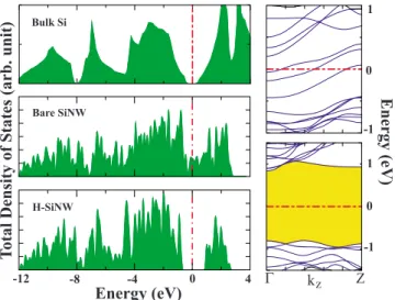
The cohesive energy is calculated as 4.24 eV, which is 0.40 eV less than that of the bulk Si crystal. While bare SiNW is metallic due to the dangling bonds on the surface, it becomes semiconductor with a direct band gap of 1.7 eV when the dangling bonds are saturated with H atoms. In view of the fact that GGA underestimates the band gaps, the sys-tem may have a wider direct band gap, which is very conve-nient for optoelectronic applications.27 The total density of
states 共TDOS兲 and energy band diagrams are illustrated in Ideal SiNW Bare SiNW H-SiNW
Si-Si
distance
distribution
(arb.
unit)
0 0.6 0 1 0 6distance (A)
1 2 3 4 5 6 7 oCross Section Side View
FIG. 1. 共Color online兲 Cross section and side views of opti-mized bare SiNW共uppermost two panels兲 and hydrogen passivated SiNW 共lower two panels兲. Side views of the figures are given in three unit cells for clarity. On the right panels, the Si-Si distance distribution up to the sixth nearest neighbors is indicated for ideal SiNW, as cut from bulk crystal, optimized bare SiNW, and hydro-genated SiNW. The dotted line in the third panel represents the H–Si bond population.
Fig.2. For the sake of comparison, TDOS of bulk Si is given on the left upmost panel.
IV. SINGLE ATOM ADSORPTION A. Structure and energetics
Having discussed the structural and electronic properties of bare and H-SiNW, we now present a systematic analysis of the doping of various elements from group IIIA共Al, Ga兲, group IVA共C, Si, Ge兲, group VA 共As, N, P兲, group VIA 共Te兲 and also Pt as a TM element. In semiconductor physics, the doping normally indicates the minute concentration of for-eign共impurity兲 atoms implemented substitutionally or inter-stitially into the crystal with an average nearest neighbor distance of several lattice parameters. An impurity state that cannot couple with the neighboring ones becomes localized 共isolated兲 at the impurity site. The electron-electron interac-tion, the resulting dielectric constant ⑀o, and the effective mass m쐓 of the band electrons determine the energy levels relative to the band edges and the effective radius of the donors or acceptors. However, the situation may be different for doped H-SiNWs because ⑀o and m쐓 undergo a change due to size and dimensionality effects. Moreover, local envi-ronment, as well as coordination of an impurity in H-SiNW, can be different from its counterpart in bulk Si crystal. For example, an impurity can be adsorbed on the surface or sub-stitute a Si atom either at the surface or in the core region. Here, we simulated the effect of doping by adsorbing a single impurity adatom to the surface either in every unit cell 共having nearest neighbor distance ᐉn,n= co and N = 57兲 or in every two unit cells共having ᐉn,n= 2coand N = 114兲. While the significant coupling in the case of high concentration leads to the formation of the bands, owing to the negligible coupling in the case of low concentration, the dopant adatom yields flat impurity bands. These flat bands may be taken to repre-sent states of an isolated impurity. In order to find the
ener-getically most favorable configuration of adatoms, we first consider six possible initial adsorption sites28 on the surface
of the nanowire, as described in Fig.3. We initially place the adatom at one of these sites and fully relax the whole system in order to obtain the energetically most favorable configu-ration. In the relaxation process, structural deformations and also bond breaking of Si-Si or Si-H are allowed. The results that we have obtained from present calculations are summa-rized in Table I. The binding energy of elements are calcu-lated from the following expression:
Eb= ET关H-SiNW共N兲兴 + ET关A兴 − ET关H-SiNW共N兲 + A兴, 共1兲 where ET关H-SiNW共N兲+A兴 is the total energy of adatom A absorbed to H-SiNW共N兲, ET关H-SiNW共N兲兴 is the total energy of H-SiNW共N兲, and ET关A兴 is either the spin-polarized or spin-unpolarized energy of the adsorbed atom calculated within the same supercell.29 In the case of single unit cell calculations with N = 57, the distance between adatoms is ᐉn,n= 5.38 Å so that the interaction may not be negligible. For double cell calculations, csc=ᐉn,n= 10.76 Å and N = 114. For all the elements under consideration, Ebis considerably high, which indicates a chemical interaction between adatom and H-SiNW.
We found that the energetically most favorable adsorption site depends on the group of the Periodic Table that the ada-tom belongs to. For example, site MH is found to be favored by the group IIIA elements共namely, Al, Ga兲. On the other hand, elements of groups IVA, VA, and VIA prefer site B. Platinum, being a TM element, prefers site SH after atomic relaxation. First row elements, C and N, having the smallest radius among all elements studied here, are adsorbed with a high binding energy Eb= 8.06 and 8.71 eV, respectively. These two atoms first break Si–Si bond to form Si–A–Si bond and also attract the H atom of the neighboring Si–H
Z Γ kz 1 0 -1 1 0 -1 Energy (eV ) -12 -8 -4 0 4 Energy (eV) Total Dens ity ofS tates (arb. un it ) Bare SiNW H-SiNW Bulk Si
FIG. 2.共Color online兲 The left panels display the TDOS of bulk Si, optimized bare SiNW, and optimized H-SiNW. The right panels are the energy band diagrams for the optimized bare and hydrogen-ated silicon nanowires. The energy gap of semiconducting H-SiNW is shaded. The zero of energy is taken at the Fermi level.
MH MP SH
SP B T
FIG. 3. 共Color online兲 Possible adsorption sites of the adatom 共impurity兲 at the surface. These sites are, respectively, the 共1兲 hol-low site of the surface hexagon at the concave part of the cross section共see Fig.1兲 共MH兲, 共2兲 hollow site of the surface pentagon at the concave part of the cross section共MP兲, 共3兲 hollow site of the surface hexagon at the convex part of the cross section共SH兲, 共4兲 hollow site of the surface pentagon at the convex part of the cross section共SP兲, 共5兲 bridge site of hexagon at the convex part of the cross section共B兲, and 共6兲 top sites 共T兲.
TABLE I. Initial positions of the impurities共adatoms兲 are indicated with abbreviations such as MH, MP,
SH, SP, B, and T, as described in Fig.3. Single cell共double cell兲 signifies that the periodic nearest neighbor distance of the adatoms isᐉn,n= co共ᐉn,n= 2co兲. Final optimized configurations are denoted, for example, as
→MH. Superscript b means that adatom breaks Si-Si bond共s兲 in the vicinity of its initial position. Subscript h indicates breaking and binding of hydrogen atom by the adatom. Ebup 共Ebsp兲 and Ebb correspond to the impurity binding energy relative to spin-unpolarized共spin-polarized兲 free atom and bulk energies of impurity atom, respectively. d shows the distance between adatom and nearest neighbor Si atoms.
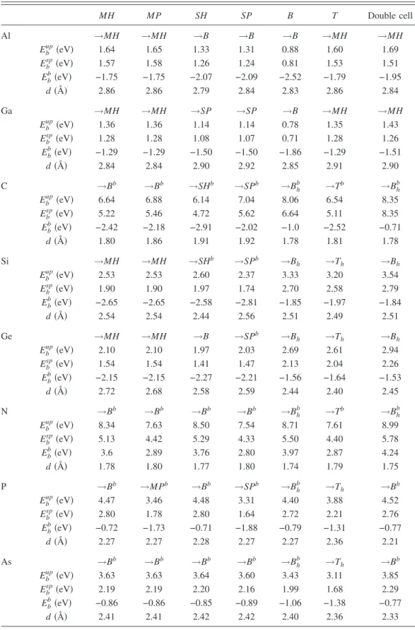
MH MP SH SP B T Double cell Al →MH →MH →B →B →B →MH →MH Ebup共eV兲 1.64 1.65 1.33 1.31 0.88 1.60 1.69 Ebsp共eV兲 1.57 1.58 1.26 1.24 0.81 1.53 1.51 Ebb共eV兲 −1.75 −1.75 −2.07 −2.09 −2.52 −1.79 −1.95 d共Å兲 2.86 2.86 2.79 2.84 2.83 2.86 2.84 Ga →MH →MH →SP →SP →B →MH →MH Ebup共eV兲 1.36 1.36 1.14 1.14 0.78 1.35 1.43 Ebsp共eV兲 1.28 1.28 1.08 1.07 0.71 1.28 1.26 Ebb共eV兲 −1.29 −1.29 −1.50 −1.50 −1.86 −1.29 −1.51 d共Å兲 2.84 2.84 2.90 2.92 2.85 2.91 2.90 C →Bb →Bb →SHb →SPb →B h b →Tb →B h b Ebup共eV兲 6.64 6.88 6.14 7.04 8.06 6.54 8.35 Ebsp共eV兲 5.22 5.46 4.72 5.62 6.64 5.11 8.35 Ebb共eV兲 −2.42 −2.18 −2.91 −2.02 −1.0 −2.52 −0.71 d共Å兲 1.80 1.86 1.91 1.92 1.78 1.81 1.78 Si →MH →MH →SHb →SPb →B h →Th →Bh Ebup共eV兲 2.53 2.53 2.60 2.37 3.33 3.20 3.54 Ebsp共eV兲 1.90 1.90 1.97 1.74 2.70 2.58 2.79 Ebb共eV兲 −2.65 −2.65 −2.58 −2.81 −1.85 −1.97 −1.84 d共Å兲 2.54 2.54 2.44 2.56 2.51 2.49 2.51 Ge →MH →MH →B →SPb →B h →Th →Bh Ebup共eV兲 2.10 2.10 1.97 2.03 2.69 2.61 2.94 Ebsp共eV兲 1.54 1.54 1.41 1.47 2.13 2.04 2.26 Ebb共eV兲 −2.15 −2.15 −2.27 −2.21 −1.56 −1.64 −1.53 d共Å兲 2.72 2.68 2.58 2.59 2.44 2.40 2.45 N →Bb →Bb →Bb →Bb →Bhb →Tb →Bhb Ebup共eV兲 8.34 7.63 8.50 7.54 8.71 7.61 8.99 Ebsp共eV兲 5.13 4.42 5.29 4.33 5.50 4.40 5.78 Ebb共eV兲 3.6 2.89 3.76 2.80 3.97 2.87 4.24 d共Å兲 1.78 1.80 1.77 1.80 1.74 1.79 1.75 P →Bb →MPb →Bb →SPb →B h b →T h →Bb Ebup共eV兲 4.47 3.46 4.48 3.31 4.40 3.88 4.52 Ebsp共eV兲 2.80 1.78 2.80 1.64 2.72 2.21 2.76 Ebb共eV兲 −0.72 −1.73 −0.71 −1.88 −0.79 −1.31 −0.77 d共Å兲 2.27 2.27 2.28 2.27 2.27 2.36 2.21 As →Bb →Bb →Bb →Bb →B h b →T h →Bb Ebup共eV兲 3.63 3.63 3.64 3.60 3.43 3.11 3.85 Ebsp共eV兲 2.19 2.19 2.20 2.16 1.99 1.68 2.29 Ebb共eV兲 −0.86 −0.86 −0.85 −0.89 −1.06 −1.38 −0.77 d共Å兲 2.41 2.41 2.42 2.42 2.40 2.36 2.33
bond to form A–H bond共i.e., C–H or N–H兲 specified as Bh b configuration in TableI. Si and Ge adatoms are adsorbed at the bridge position above the Si-Si bond without any signifi-cant deformation at the underlying Si nanowire but break the Si–H bond and bind the freed H atom. This adsorption con-figuration is specified as Bh. P, As, and Te are adsorbed at site
Bb, but they cannot break the neighboring Si–H bond. Pt has also high binding energy 共5.24 eV兲. Unlike the other ele-ments, Pt has moved inward after relaxation. Besides, Pt–Si bond length is measured as 2.5 Å, which is comparable to the Pt–Pt bond distance共2.8 Å兲 in bulk Pt. The binding en-ergies with respect to the element’s bulk cohesive energy are always negative except for N. This means that nitrogen dop-ing is an exothermic process in which energy is given out from the system. Note that N is the only element studied in this work, being in the gaseous state at room temperature, while others are in solid state. Interestingly, there exists a trend in binding energies of elements within the same group in such a way that it decreases as the radius of the element increases. While the distance of Al and Ga to the nearest Si atoms is d = 2.9 Å, this distance ranges between 2.3 and 2.5 Å for other elements except C and N. Carbon and nitro-gen, having the smallest radius among other impurities, have the smallest distance to the nearest neighbor Si atoms.
In the double cell calculations共ᐉn,n= 2co兲, we considered only the most energetic sites determined in single cell calcu-lations. By placing the adatom to the same position in every two cells, we relaxed the whole system to minimize the total energy. Results are given in the last column of TableI. After the atomic relaxation, we observed similar effects, such as breaking of Si–Si and Si–H bonds and also binding of H by the same adatoms discussed in single cell calculations. The trend in binding energy of adatom which decreases as it moves down within the same group elements is also ob-served in double cell calculations. Furthermore, the binding energies which are calculated by using Eq.共1兲 in double cell slightly increase as compared to the single cell results. Asᐉnn increases from 5.38 to 10.76 Å, the interaction between ada-toms reduces, whereby adatom-wire interaction is enhanced. Eb, with respect to bulk cohesive energies, remains negative except for nitrogen again. The nearest adatom-Si distance, d does not significantly change from single cell values.
Finally, we note that binding energies in Table I corre-sponding to the same final optimized adsorption geometry which initiates from different adsorption sites may differ slightly. This is due to the different paths of the impurity atom between the final and different initial configurations, whereby the final geometry may deviate slightly from the minimum total energy configuration. Here, the highest value of Ebhas to be taken as the binding energy of the final, most energetic adsorption site. However, there are significant en-ergy differences between the same B共or Bb兲 optimized final adsorption geometry. This originates from the bridge sites of the hexagonal or pentagonal rings.
B. Electronic properties
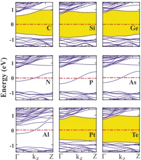
We first consider adatom adsorption at high concentration with ᐉn,n= co, where the electronic structure of H-SiNW is affected considerably. The energy band diagrams are illus-trated in Fig.4. Semiconducting H-SiNW becomes metallic upon adsorption of IIIA and VA elements, which have an odd number of valence electrons. For these systems, one nonde-generate half-filled band crosses the Fermi energy EF. Ac-cording to the band decomposed charge density analysis, these bands originate from the impurity atom. The dispersion of these bands indicate a non-negligible coupling between adatoms. The quantum ballistic conductance30of such an
in-finite metallic wire at small bias is G = 2e2/h. The conduc-tance of the finite wire is, however, smaller than 2e2/h due to connections to the electrode. For the other elements which have an even number of valence electrons, the wire remains semiconducting with modified band gaps. C and Pt doped H-SiNWs have again a direct band gap of 1.17 and 1.36 eV, respectively, whereas Ge, Si, and Te atoms change H-SiNW from the direct band gap to the indirect band gap of 1.46, 1.41, and 1.54 eV, respectively.31 Commonly, we observe
that the band gap value decreases after the adsorption of the adatom.
Next, we examine the electronic structure at low concen-tration of the adatom obtained from double cell calculations withᐉn,n= 2co. The corresponding energy band structures are presented in Fig.5. Due to the reduced interaction between adatoms, the dispersion of the bands near EF is low. These TABLE I. 共Continued.兲 MH MP SH SP B T Double cell Te →Bb →MPb →Th →Bb →Th →Th →Bb Ebup共eV兲 2.94 2.08 2.78 2.02 2.73 2.74 2.86 Ebsp共eV兲 2.42 1.56 2.26 1.50 2.20 2.22 2.29 Ebb共eV兲 0.019 −0.85 −0.14 −0.91 −0.20 −0.19 −0.20 d共Å兲 2.52 2.69 2.54 2.51 2.53 2.54 2.52 Pt →MH →MPb →SH →SPb →B h →T →SH Ebup共eV兲 5.24 5.03 5.49 5.07 4.38 4.72 5.63 Ebsp共eV兲 4.99 4.79 5.24 4.82 4.14 4.47 5.30 Ebb共eV兲 −0.53 −0.74 −0.28 −0.70 −1.38 −1.05 −0.24 d共Å兲 2.42 2.39 2.48 2.40 2.38 2.38 2.48
bands may be assumed to correspond to the isolated impurity levels. At very low concentration共which cannot be treated by the present method兲, the isolated impurity levels do not coincide with the Fermi level.32 Interestingly, while the im-purity level that coincides with the Fermi energy is closer to the valence band for the case of P and As doped H-SiNW共114兲, it lies at the middle of the band gap of the N
doped nanowire. Surprisingly, Al doping causes energy lev-els to shift closer to the conduction band. The location of impurity states in the band gap occurs in a reverse order as compared to the n-type共N, P, As兲 and p-type 共Al, Ga兲 dop-ants in bulk Si crystal. In fact, Singh et al.10have studied the
effects of substitutional P impurity on the electronic and atomic structures of H-SiNW共along the 关110兴 direction and having a square cross section兲 using a similar ab initio method. The Fermi level was seen to shift toward the con-duction band while making the nanowire n type. This situa-tion is explained by the fact that in the present case, the adatoms are simply absorbed on the surface of H-SiNW. Similar to the single cell analysis, C and Te doped H-SiNW共114兲 have again direct and indirect band gaps, re-spectively. On the other hand other elements change the nanowire from the direct band gap into the indirect band gap or vice versa. Besides, the energy gap values are increased as compared with the single cell results. Although n- or p-type impurity effects cannot be observed in the case of adsorbed adatom type, one can tune the band gap of the doped nano-wire easily. This is a promising result for optoelectronic ap-plications. However, it should be noted that the effect of impurity on the band gap diminishes as the concentration of adatom decreases and, hence, ᐉn,nbecomes several co. The band decomposed charge density analysis clearly indicates the character of the impurity level. These bands belong to p orbitals of dopant atoms.
V. SUBSTITUTION
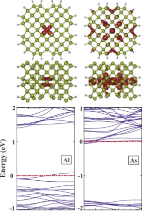
In addition to adatom adsorption on the surface of SiNW, substitutional impurities such as Al and As have also been examined. To this end, one Si atom in the core or on the surface of H-SiNW共114兲 was replaced with either Al or As atom. The substitution energy is calculated as follows:
Es= ET关H-SiNW共114兲兴 + ET关S兴
− ET关H-SiNW共113兲 + S兴 − ET关Si兴, 共2兲 where S denotes the free impurity atom, and ET关H-SiNW共113兲+S兴 is the total energy of the optimized system where one Si atom is replaced by S. After the full relaxation of the system, surface configurations were seen to be more favorable when compared with the core ones, in agreement with earlier calculations dealing with B and P doped Si nanowires.10,11The substitution energies of dopants relative to the spin-unpolarized共spin-polarized兲 dopant free atom energy and their bulk energies are given in Table II. The energy band diagrams are presented in Figs. 6 and 7 together with their charge analysis. As one can see, it is possible to make p-type共n-type兲 silicon nanowire by doping with Al 共As兲 atom substitutionally. The isosurface charge analysis presented in Fig.6displays p-type orbital character-istics for the levels crossing the Fermi energy. The nonde-generate band with negligible dispersion originates mainly from Al orbitals and is reminiscent of the acceptor state at very low Al concentration. On the other hand, a hybridized state which is composed of As and its nearest neighbor Si atoms is obtained for the As doped nanowire. Flat As impu-Al C Si N Pt Te As Ge P Energy (eV) -1 0 1 -1 0 1 -1 0 1 Z Γ kz Γ kz Z Γ kz Z
FIG. 4.共Color online兲 Energy band structures of adatom 共impu-rity兲 adsorbed H-SiNW. The distance between adjacent impurity atoms is ᐉn,n= co= 5.38 Å. The energy gaps of semiconducting
structures are highlighted. The dash-dotted line represents the Fermi level. Note that owing to the significant adatom-adatom interaction, the width of the impurity bands is in the range of 0.5– 1 eV.
-1 0 1 Al C Si Pt Te Energy (eV) Z Γ kz Γ kz Z Ge Γ kz Z -1 0 1 N P As -1 0 1
FIG. 5.共Color online兲 Energy band structures of adatom 共impu-rity兲 adsorbed H-SiNW共114兲 with ᐉn,n= 2co= 10.76 Å. The energy
gaps of semiconducting structures are again highlighted. The flat bands which line up with the Fermi energy are reminiscent of iso-lated impurity levels.
rity bands occur near the conduction band edge, attributing an n-type character to the dopant. At very low As concentra-tion, these flat bands become isolated donor states near the conduction band edge. For the case of surface substitutional doping, the isosurface charge analysis of those nondegener-ate single levels crossing the Fermi energy are again purely p-type dopant states. We note, however, that energies relative to the band edges and characters of these donor and acceptor states are closely related to the configuration of the corre-sponding substitutional impurity.
VI. DISCUSSION AND CONCLUSIONS
In this paper, we presented a systematic study of the effect of doping of silicon nanowire by several impurity atoms. We
took a hydrogenated Si nanowire as prototype and investi-gated the adsorption and substitution onto the surface, as well as the substitution of impurity atom in the core. The adsorption of impurity atom on the surface has been treated in the high concentration共one adatom per unit cell of 57 Si atoms兲 and “low” concentration 共one adatom per two unit cells of 114 Si atoms兲 limits. The usual band theory yields impurity bands for both concentration limits, the high con-centration bands being dispersive and the low concon-centration bands being flat. The latter flat bands have been taken as representative of single impurity levels. Our analysis reveals that SiNW surface impurity sites are very active and strongly interacts with IIIA, IVA, VA, and VIA elements. While IIIA elements 共Al, Ga兲 prefer to be at the center of the middle hexagon and do not distort the SiNW surface, the elements in other groups break the Si–Si bond共s兲 of the nanowire. C and N even break Si–H bond and bind the hydrogen atom to themselves. Different from the elements in groups IIIA, IVA, VA, and VIA, Pt prefers the hollow site of the hexagon being in the same plane as Si atoms. Initially semiconducting H-SiNW becomes metallic when IIIA and VA elements are
TABLE II. Substitution energy of the substitutional impurities共Al and As兲. Esup, Essp, and Esbare defined as in the caption of TableIand Eq.共2兲.
Esup 共eV兲 Essp 共eV兲 Esb 共eV兲 Esup 共eV兲 Essp 共eV兲 Esb 共eV兲 Alsurface −2.72 −2.15 −0.97 Assurface −1.40 −2.22 −0.65 Alcore −3.00 −2.44 −1.26 Ascore −1.53 −2.35 −0.78 -1 0 1 2 -1 0 1 -2 Energy (eV) Al As
FIG. 6. 共Color online兲 Si atom in the core of H-SiNW共114兲 is replaced with impurity atom共Al or As兲. On the left, Al replaced one of the core Si atoms. The charge density graph is given at the top, indicating p-orbital characteristics. The energy band structure at the bottom indicates a p-type behavior. On the right, the charge density graph and energy band structure of As replacing one of the core Si atoms are presented. All these analyses are realized for the double unit cell. -1 0 1 2 Energy (eV) Al 0 -1 -2 1 As Γ kz Z Γ kz Z
FIG. 7.共Color online兲 Si atom on the surface of H-SiNW共114兲 is replaced with either Al or As atom. p-orbital characteristics of impurity states and p-type共Al兲 and n-type 共As兲 behaviors of semi-conducting are clearly seen.
adsorbed in the high concentration limit. However, it remains semiconducting with a modified band gap when doped with other elements that have even number of valence electrons. Similar trends are also obtained in the low concentration limit. Due to the reduced adatom-adatom interaction, disper-sionless impurity bands are obtained. The band decomposed charge density analysis indicates that these levels originate from doping elements. H-SiNW semiconductor can be modi-fied as a p type and an n type through substitution of Al and As, respectively. In view of the above results, one can con-template that metallic, n and p-type zones or any sequence and size of them can be generated according to a desired device functionality. This way, various types of devices and a
metallic interconnect between them can be realized using the same Si nanowire. In particular, metal-semiconductor junc-tions shall easily be produced. It is expected that the above trends exist in other H-SiNWs with N⬎57. In conclusion, our results indicate that the electronic properties of SiNW can be modified by single atom adsorption according to the desired properties and can be used in nanoscale device ap-plications.
ACKNOWLEDGMENT
Part of the computations has been performed using the ULAKBİM High Performance Computer Center.
1Y. Cui, Z. Zhong, D. Wang, W. U. Wang, and C. M. Lieber, Nano Lett. 3, 149共2003兲.
2Y. Huang, X. F. Duan, and C. M. Lieber, Small 1, 142共2005兲. 3X. F. Duan, Y. Huang, R. Agarwal, and C. M. Lieber, Nature
共London兲 421, 241 共2003兲.
4D. D. D. Ma, C. S. Lee, F. C. K. Au, S. Y. Tong, and S. T. Lee, Science 299, 1874共2003兲.
5R. Rurali and N. Lorente, Phys. Rev. Lett. 94, 026805共2005兲. 6A. K. Singh, V. Kumar, R. Note, and Y. Kawazoe, Nano Lett. 5,
2302共2005兲.
7Y. Zhao and B. Yakobson, Phys. Rev. Lett. 91, 035501共2003兲; S. Ismail-Beigi and T. Arias, Phys. Rev. B 57, 11923共1998兲. 8R. Q. Zhang, Y. Lifshitz, D. D. D. Ma, Y. L. Zhao, Th.
Frauen-heim, S. T. Lee, and S. Y. Tong, J. Chem. Phys. 123, 144703 共2005兲.
9P. W. Leu, B. Shan, and K. Cho, Phys. Rev. B 73, 195320共2006兲. 10A. K. Singh, V. Kumar, R. Note, and Y. Kawazoe, Nano Lett. 6,
920共2006兲.
11M. V. Fernandez-Serra, Ch. Adessi, and X. Blase, Phys. Rev. Lett.
96, 166805共2006兲.
12Y. Cui, Q. Q. Wei, H. K. Park, and C. M. Lieber, Science 293, 1289共2001兲.
13X. T. Zhou, J. Q. Hu, C. P. Li, D. D. D. Ma, C. S. Lee, and S. T. Lee, Chem. Phys. Lett. 369, 220共2003兲.
14J. Hahm and C. M. Lieber, Nano Lett. 4, 51共2004兲.
15E. Durgun, D. Cakir, N. Akman, and S. Ciraci, arXiv:0704.0109. 16H. Sellier, G. P. Lansbergen, J. Caro, S. Rogge, N. Collaert, I. Ferain, M. Jurczak, and S. Biesemans, Phys. Rev. Lett. 97, 206805共2006兲.
17S. Sirichantaropass, V. M. Garcia-Suarez, and C. J. Lambert, e-print arXiv:cond-mat/0611128.
18M. C. Payne, M. P. Teter, D. C. Allen, T. A. Arias, and J. D. Joannopoulos, Rev. Mod. Phys. 64, 1045共1992兲.
19Numerical computations have been carried out usingVASP soft-ware. G. Kresse and J. Hafner, Phys. Rev. B 47, R558共1993兲; G. Kresse and J. Furthmuller, ibid. 54, 11169共1996兲.
20W. Kohn and L. J. Sham, Phys. Rev. 140, A1133 共1965兲; P. Hohenberg and W. Kohn, Phys. Rev. 136, B864共1964兲.
21D. Vanderbilt, Phys. Rev. B 41, R7892共1990兲.
22We used the following configurations for the atomic pseudopo-tentials: Al and Ga: s2p1; C, Si, and Ge: s2p2; N, P, and As: s2p3; Te: s2p4; Pt: s1d9.
23J. P. Perdew, J. A. Chevary, S. H. Vosko, K. A. Jackson, M. R. Pederson, D. J. Singh, and C. Fiolhais, Phys. Rev. B 46, 6671 共1992兲.
24M. Methfessel and A. T. Paxton, Phys. Rev. B 40, 3616共1989兲. 25H. J. Monkhorst and J. D. Pack, Phys. Rev. B 13, 5188共1976兲. 26In the present study, H-SiNW is obtained in following sequences:
First, the ideal SiNW is cut from the ideal, tetrahedrally coordi-nated bulk Si crystal. Ideal and bare SiNW is then fully opti-mized. The structure of this bare nanowire is shown in Fig.1. This optimized bare SiNW is passivated with H atoms and even-tually optimized again. Note that this sequence leads to elec-tronic properties different from the sequence where the ideal bare SiNW is passivated and then optimized.
27According to the GW corrections carried out by X. Zhao, C. M. Wei, L. Yang, and M. Y. Chou, Phys. Rev. Lett. 92, 236805 共2004兲, the actual band gap of H-SiNW共57兲 is estimated to be ⬃2.3 eV.
28There are other sites on the surface for the adsorption of atoms that are left out of the scope of the present study. For example, in addition to the bridge sites of surface hexagons共BH兲, there are two types of bridge sites of surface pentagons, namely, one be-tween the two adjacent pentagons and the other one bebe-tween the adjacent hexagon and pentagon. Our test calculations showed that these two sites are not stable sites for adatom.
29In this way, the adatom-adatom coupling is excluded in the value of binding energy Eb.
30Note that such a half-filled metallic band is vulnerable to the Peierls distortion.
31In these band gap values, the GW self-energy corrections are not taken into account.
32Statistical calculations based on the law of mass action关see, for example, C. Kittel, Introduction to Solid State Physics, 7th ed. 共Wiley, New York, 1996兲兴 at low concentration and finite tem-perature indicate that the chemical potential shifts from the iso-lated impurity levels.