The focusing effect of graded index photonic crystals
H. Kurt, E. Colak, O. Cakmak, H. Caglayan, and E. Ozbay
Citation: Appl. Phys. Lett. 93, 171108 (2008); View online: https://doi.org/10.1063/1.3009965
View Table of Contents: http://aip.scitation.org/toc/apl/93/17
Published by the American Institute of Physics
Articles you may be interested in
Self-focusing media using graded photonic crystals: Focusing, Fourier transforming and imaging, directive emission, and directional cloaking
Journal of Applied Physics 110, 053103 (2011); 10.1063/1.3630116
Design and experimental evidence of a flat graded-index photonic crystal lens
Journal of Applied Physics 114, 083105 (2013); 10.1063/1.4817368
High efficiency of graded index photonic crystal as an input coupler
Journal of Applied Physics 105, 103708 (2009); 10.1063/1.3130403
Graded photonic crystals curve the flow of light: An experimental demonstration by the mirage effect
Applied Physics Letters 92, 133501 (2008); 10.1063/1.2901684
A cylindrical optical black hole using graded index photonic crystals
The focusing effect of graded index photonic crystals
H. Kurt,1,a兲 E. Colak,2O. Cakmak,2H. Caglayan,2and E. Ozbay21Department of Electrical and Electronics Engineering, TOBB University of Economics and Technology,
06560 Ankara, Turkey
2Nanotechnology Research Center-NANOTAM, Department of Physics, and Department of Electrical
and Electronics Engineering, Bilkent University, Bilkent, 06800 Ankara, Turkey
共Received 3 September 2008; accepted 7 October 2008; published online 29 October 2008兲 We describe an approach to implement graded index 共GRIN兲 structures using two-dimensional photonic crystals共PCs兲. The lattice spacing along the transverse direction to propagation is altered and we show, both theoretically and experimentally, that such a spatial perturbation is an effective way to obtain GRIN PC. The response of the structure to spatially wide incident beams is investigated and strong focusing behavior is observed. The large spot size conversion ratio can be attainable and is mainly limited by the finite size of the structure. The designed GRIN PC shows promise for use in optical systems that require compact and powerful focusing elements compared to the traditional bulky lenses. © 2008 American Institute of Physics. 关DOI:10.1063/1.3009965兴
The photonic crystals 共PCs兲 are multidimensional peri-odic dielectric structures with their spatial periperi-odicity at the same length scale as the subwavelength of light. If the operating frequency of the incident light is within the prohibited frequency region, called the photonic band gap, then PC may act as a mirror reflecting the entire incoming wave.1The periodic nature of the crystal along with the high-index contrast dielectric materials governs some of the re-markable properties of PCs, such as self-collimation and superprism.2–6The pure periodicity of PCs can be broken by introducing spatial perturbations in terms of point- or line-type defects. As a result, artificially created modes can be localized in a small area or guided through waveguides with sharp bends.7–12
In addition to guiding and confining the light, focusing it to a small spot size is an imperative procedure in photonics. The bulky lenses with curved surfaces have to be replaced with more compact ones. PCs also possess potential for this kind of application. Plano-concave lenses that are obtained with PCs that have a negative effective index and left-handed electromagnetic properties have been proposed to focus the light.13–18 There have been various other studies addressing the different applications of PCs that certain types of struc-tural modifications are introduced. The self-collimation, fo-cusing, mirage, and superbending effects were explored pre-viously with the graded PCs.19–22The beaming effect from a corrugated concave surface of PCs was studied in Ref.23, in which the pattern of the emitted beam demonstrated the fo-cusing effect. In the present study, we consider index based confinement using a graded index共GRIN兲 PC by modulating the lattice spacing of the crystal. The average index amount 共the dielectric filling factor兲 is larger at the center of the PC than that at the sides, in which the incident wave with a planar wave front converges toward the central region. The surfaces of the GRIN PC are flat and the complete structure is very compact. We theoretically show, and experimentally prove, that only a few columns of PCs are capable of strongly focusing spatially wide beams to a narrow area. The appeal of GRIN PC encourages us by using it as an interface
device that can act as a coupler by enhancing the coupling efficiency of wide input beams to narrow PC waveguides. However, this aspect of the GRIN PC will be pursued in another study.
There can be other ways of achieving GRIN variation rather than modulating the lattice spacing. The radii of the rods or the refractive index of the dielectric rod are the pa-rameters to be engineered in order to have an index gradient along certain directions. The changes in the rod radii require precise and small increments. Furthermore, it limits the range of the index gradient that can be achieved. Similarly, the index changes of the rods require different materials to be used. As a result, when a comparison is made among the choices, we can state that the selected method that uses the lattice spacing seems to be more practical than the others. Therefore, in the present study we modulate the lattice spac-ing in order to implement GRIN PC.
The advances in fabrication technology allow for the fabrication of them in the optical frequency regime. At the same time, the scalability of Maxwell’s equations makes it possible to scale the wavelength to any spectral region. Since targeting the microwave frequencies lifts some of the tech-nological and practical burdens, the experimental work is performed at the microwave regime.
The structure under study is composed of aluminum di-electric rods in an air background. The refractive index is taken to be n = 3.13 and the radius of the rod is r = 0.22a, where a is the lattice constant. The unmodified PC structure has a square-lattice crystal but the lattice spacing along the
y-direction is altered. The GRIN PC geometry under study is
shown in Fig.1共a兲. It is a two-dimensional PC, in which the polarization is taken to be TM共electric field is along the rod axis兲. The TE polarization is not considered in the study. The lattice spacing along the y-direction is changed, in turn keep-ing the spackeep-ing in the x-direction constant at a. Half of the GRIN PC that is surrounded by the dashed lines in Fig. 1共a兲 is enlarged and is shown in Fig. 1共b兲. The other half of the GRIN PC is the exact replica of this enlarged portion. The spatial increment 共⌬yi+1−⌬yi兲 occurs at every row of the
dielectric rods, where the subscript i takes the values from 0 to 6. The distances between each set of rows are labeled as 2⌬yi. The rows closest to the central part have 2⌬y0 a兲Electronic mail: [email protected].
APPLIED PHYSICS LETTERS 93, 171108共2008兲
= 0.75a and the incremental step is taken to be 0.15a. This means that 2⌬y1= 1.3a, 2⌬y2= 1.6a, etc. The reason behind this selection will be explained later. The width of the GRIN PC is 26.54a and the length of it is varied in order to study the focusing mechanism with respect to the column numbers. In the figure, there are N = 8 columns that make the length become共N−1兲a.
The finite-difference time-domain 共FDTD兲 method is carried out to observe the field propagation throughout the computational domain, which is terminated by the perfectly matched layer absorbing boundary condition.24 The input source is a spatially broad modulated Gaussian pulse with a center frequency at a/=0.38. This center frequency is within the waveguide modes of a regular PC waveguide 共PCW兲 that is obtained by removing one row of rods. In the present study, only a GRIN PC structure is investigated, but the integration of GRIN PC with PCWs will be studied in another work.
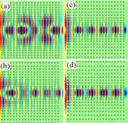
In order to decide the value of the incremental step value, four cases 共0.05a, 0.10a, 0.15a, and 0.20a兲 are se-lected and a comparison is made among them. Figure 2
shows the steady-state electric field map of these cases when a spatially broad Gaussian pulse is sent to different GRIN PC. As we can see in Figs.2共a兲and2共b兲, small increments of 0.05a and 0.10a have less focusing power. As a result, the beam is partly focused. When we increase the increment step from 0.10a to 0.150a, the field becomes strongly focused at the focal point and the beam pattern shows small and peri-odic oscillations. There is not much change in the field’s focusing behavior if the increment step is increased from 0.15a to 0.20a. As a result, 2共⌬yi+1−⌬yi兲=2共0.15兲a is
se-lected by considering the need to have a compact structure. The focusing behavior of the designed GRIN PC with respect to the number of columns N is studied next. In this part, the number of the columns is increased and the nature of the spatially broad incident beam is analyzed. The full width at half maximum 共FWHM兲 value of the beam at the focal point of the GRIN PC is recorded. The incident beam has a FWHM value of 10.8a. We can clearly see in Fig.3共a兲
that one layer hardly shows the respective focusing behavior. As the layer number increases to 2, the focusing effect of GRIN PC becomes more apparent. The FWHM values show little change after the layer number exceeds 3. The decre-ment in the FWHM value means that the maximum peak of the field at the focal point increases and is also a measure of the focusing power. From the figure, we can claim that one may not need a very large PC structure in order to focus a wide beam to a small area. The power of the focusing be-havior can be quantified by looking at the spot size conver-sion ratio, which is around 8.4. By sending even spatially broader pulses to GRIN PC in turn produces tightly focused beams. As a result, the spot size conversion ratio increases. We should note here that the finite size of the GRIN PC along the y-direction restricts the sending of spatially very wide pulses. The photonic devices that produce a small spot size ratio play a crucial role, especially for interconnect de-vices. Figure 3共b兲 shows the amplitude profile of the beam for three cases. The broadest profile with the blue line rep-resents the input pulse without GRIN PC. The green and red lines indicate the beam profiles at the exit side of the GRIN PC with N = 4 and N = 6, respectively. The strong focusing effect and small changes in the FWHM values of the beams after focusing occurs can be observed from the figure.
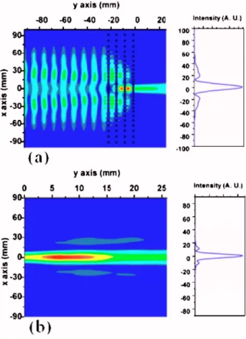
The magnitude of the steady-state electric field of the GRIN PC structure with four columns is monitored with the FDTD method. The result is shown in Fig.4共a兲. The spatially wide input beam can be seen at the input side of the GRIN PC. The input beam reduces its spatial width considerably after traveling through a few columns of the dielectric rods and focuses to the central part of the structure. It remains confined within this central area. The experimental charac-terization of the designed GRIN PC, which is composed of aluminum rods with a = 7 mm, is performed at 18 GHz by using a network analyzer as well as horn and monopole an-tennas. The horn antenna illuminates the structure at a dis-tance of 70 mm and one monopole antenna at the output of the GRIN PC is used to capture the field scanning area. Fig-ure4共b兲shows the measured intensity distribution at the exit side of the GRIN PC. The intensity is confined spatially to a narrow region. The measurement is in good agreement with the FDTD calculation. The cross sectional profiles of the FIG. 1. 共a兲 The schematic representation of the GRIN PCs. The lattice
spacing is increased along the y-direction and is kept constant at a along the
x-direction. The distances between each set of rows are labeled as 2⌬yi,
where the subscript i takes the values from 0 to 6.共b兲 Half of the structure surrounded by the rectangular area with the dashed line is enlarged at the right-hand side in the figure.
FIG. 2. 共Color online兲 The electric field pattern of the incident Gaussian beam at the center frequency of a/=0.38 for four cases of increments. ⌬yi+1−⌬yi= 0.05a for共a兲 and it is 0.10a, 0.15a, and 0.20a for 共b兲, 共c兲, and
共d兲, respectively.
E-fields at the focal point, 0.6 mm away from the PC
sur-face, is also presented on the right-hand sides in the figure. A flat surface GRIN PC lens is obtained by modulating the lattice spacing of the PC. The curved surfaces of the conventional convex lenses behave in a similar way but their size is bulky and smooth curved surfaces are required, which places stringent requirements on the fabrication procedure. Our approach is free from curved surfaces, the structure is compact, and it can be integrated easily with other photonic devices. Due to the high-index contrast between the dielec-tric rods and the air background, the index gradient that is obtained by modulating the lattice spacing is also quite large
compared to the traditional approaches. The presented results prove the importance of the engineering of the individual constituents of the PCs.
In conclusion, we performed the lattice space modula-tion of PCs in order to obtain GRIN structures. The focusing behavior of the designed device was analyzed, both theoreti-cally and experimentally, and indicated that a small number of columns are sufficient to focus a spatially wide beam to a narrow region. The theoretical result obtained with the FDTD method agrees well with the result of the experiment that was performed at the microwave region. We have proven that structural modification in PCs yields important features to manipulate the spatial profile of spatially wide incident beams.
1E. Yablonovitch,Phys. Rev. Lett. 58, 2059共1987兲.
2S. Y. Lin, V. M. Hietala, L. Wang, and E. D. Jones, Opt. Lett. 21, 1771 共1996兲.
3H. Kosaka, T. Kawashima, A. Tomita, M. Notomi, T. Tamamura, T. Sato, and S. Kawakami,Phys. Rev. B 58, R10096共1998兲.
4M. Notomi,Phys. Rev. B 62, 10696共2000兲.
5J. Witzens, M. Loncar, and A. Scherer, IEEE J. Sel. Top. Quantum Electron. 8, 1246共2002兲.
6L. Wu, M. Mazilu, and T. F. Krauss, J. Lightwave Technol. 21, 561 共2003兲.
7T. Asano, B.-S. Song, Y. Tanaka, and S. Noda,Appl. Phys. Lett. 83, 497 共2003兲.
8S. Fan, P. R. Villeneuve, J. D. Joannopoulos, and H. A. Hauss,Phys. Rev. Lett. 80, 960共1998兲.
9A. Mekis, J. C. Chen, I. Kurand, S. Fan, P. R. Villeneuve, and J. D. Joannopolous,Phys. Rev. Lett. 77, 3787共1996兲.
10H. Kurt and D. S. Citrin,IEEE J. Quantum Electron. 43, 78共2007兲. 11S. H. G. Teo, A. Q. Liu, M. B. Yu, and J. Singh, Photonics Nanostruct.
Fundam. Appl. 4, 103共2006兲.
12G. Manzacca, D. Paciotti, A. Marchese, M. S. Moreolo, and G. Cincotti, Photonics Nanostruct. Fundam. Appl. 5, 164共2007兲.
13E. Cubukcu, K. Aydin, E. Ozbay, S. Foteinopoulou, and C. M. Soukoulis, Phys. Rev. Lett. 91, 207401共2003兲.
14Z. Y. Li and L. L. Lin,Phys. Rev. B 68, 245110共2003兲.
15R. Meisels, R. Gajíc, F. Kuchar, and K. Hingerl,Opt. Express 14, 6766 共2006兲.
16E. Foca, H. Föll, J. Carstensen, V. V. Sergentu, I. M. Tiginyanu, F. Daschner, and R. Knöchel,Appl. Phys. Lett. 88, 011102共2006兲.
17I. Bulu, H. Caglayan, K. Aydin, and E. Ozbay,Opt. Lett. 32, 850共2007兲. 18K. Aydin, I. Bulu and E. Ozbay,Appl. Phys. Lett. 90, 254102共2007兲. 19E. Centeno and D. Cassagne, Opt. Lett. 74, 2278共2005兲.
20E. Centeno, D. Cassagne, and J. P. Albert, Phys. Rev. B 73, 235119 共2006兲.
21F. S. Roux and I. De Leon,Phys. Rev. B 74, 113103共2006兲. 22H. Kurt and D. S. Citrin,Opt. Express 15, 1240共2007兲.
23E. H. Khoo, A. Q. Liu, T. H. Cheng, J. Li, and D. Pinjala,Appl. Phys. Lett. 91, 221105共2007兲.
24A. Taflove, Computational Electrodynamics: The Finite-Difference
Time-Domain Method共Artech House, Norwood, MA, 2000兲.
FIG. 3.共Color online兲 共a兲 The FWHM values for different numbers of GRIN layers. Simulation and experimental results are shown by square and dia-mond shapes, respectively. 共b兲 Field profiles at the output side of the GRIN structure for N = 4 layers共green line兲 and N = 6 layers共red line兲. The free space profile共blue line兲 has also been added for comparison.
FIG. 4.共Color online兲 The focusing effect of the GRIN structure illuminated with a wide incident Gaussian beam at 18 GHz.共a兲 The electric field pattern obtained with FDTD for N = 4 layers. The cross section profile of the E-field at the focal point, 0.6 mm away from the PC surface, is also presented on the right-hand side.共b兲 The electric field pattern obtained experimentally by scanning the output side of the PC utilizing a monopole antenna. The cross section at the focal point is again given for convenience.