Contents lists available atScienceDirect
Optik
journal homepage:www.elsevier.com/locate/ijleo
Original research article
The electrical characteristics of ITO/CZTS/ZnO/Al and ITO/ZnO/
CZTS/Al heterojunction diodes
Serap Yiğit Gezgin
a, Hamdi Şükür Kılıç
a,b,c,⁎aUniversity of Selçuk, Faculty of Science, Department of Physics, 42031, Selçuklu, Konya, Turkey
bUniversity of Selçuk, Directorate of High Technology Research and Application Center, 42031, Selçuklu, Konya, Turkey
cUniversity of Selçuk, Directorate of Laser Induced Proton Therapy Application and Research Center, 42031, Selçuklu, Konya, Turkey
A R T I C L E I N F O Keywords: Thin film CZTS ZnO Diode PLD Photoelectric A B S T R A C T
In this study, ITO/a-CZTS/ZnO1/Al, ITO/ZnO2/a-CZTS/Al and ITO/ZnO2/c-CZTS/Al diode structures were produced by PLD technique and analysed, as well as data are presented. a-CZTS and ZnO thin films were grown as layer by layer thin films on ITO coated glass at room tem-perature and annealing process was not carried out for these samples. Morphologies and crystal structures of ZnO and a-CZTS thin films were analysed. ZnO thin films have been produced depending on an oxygen ambient gas pressure and a-CZTS thin film has been produced using low laser energies. While ZnO thin films exhibit crystal structure, a-CZTS has amorphous structure. In addition, c-CZTS thin film has also been annealed at 375 °C sulfurization temperature at which crystalline structure was obtained. Optical features of thin films were determined by UV–vis spectra and it was observed that a-CZTS and c-CZTS thin films have a high band gap and an ideal band gap, respectively. Diode structure of ITO/a-CZTS/ZnO1/Al has shown normal diode char-acteristics in dark environment and has different ideality factors for three regions in semi-loga-rithmic forward bias region. ITO/ZnO2/a-CZTS/Al diode structure has also shown a negative differential resistance and behaved like a tunnelling diode in dark environment exhibiting photoelectric effect under illuminated environment. Short circuit current density is very low, fill factor and open circuit voltage are quite high. In addition, ITO/ZnO2/c-CZTS/Al diode structure has shown some photo-electricity property under illumination conditions. The diode’s short circuit current density was found to be higher and open circuit voltage was very low. Electrical characteristics of diodes have been described in some details in this work.
1. Introduction
Cu2ZnSnS4 (also known as CZTS) is a chalcogenide material and p-type semiconductor, with a high absorption coefficient of 104cm−1and band gap about 1–1.5 eV [1]. That material is formed from low cost and non-toxic materials compared to the cost of Copper Indium Sulphide (CIS), Cadmium Tellur (CdTe) and Copper Indium Gallium Sulphide (CIGS) which have been widely used in second generation solar cells, even they are composed of toxic (such as Cd) and costly materials (such as In, Ga, Te). n-type buffer layers, such as CdS [2], Zinc Sulphide (ZnS) [3], Indium Sulphide (In2S3) [4] and Zinc Oxide (ZnO), can be used to form p-n junction characteristics in CZTS solar cells. CdS thin film has been used to form p-n heterojunction with CZTS thin film which has an adversely feature in that Cd diffuses into CZTS to form some defect structures and Cd is also toxic [5,6].
https://doi.org/10.1016/j.ijleo.2019.01.014
Received 9 October 2018; Received in revised form 10 January 2019; Accepted 10 January 2019 ⁎Corresponding author.
E-mail address:hamdisukurkilic@selcuk.edu.tr(H.Ş. Kılıç).
0030-4026/ © 2019 Elsevier GmbH. All rights reserved.
diodes were produced in this study. CZTS and ZnO (ZnO and CZTS) thin films have been grown as layer by layer thin films on ITO coated glass at room temperature by PLD. While ZnO1 thin film in ITO/a-CZTS/ZnO1/Al diode structure was produced at high oxygen gas pressure, other ZnO2 thin film in ITO/ZnO2/a-CZTS/Al and ITO/ZnO2/c-CZTS/Al diode structure was produced at low oxygen gas pressure. J–V (short circuit current density/voltage) characteristics of diode structures were obtained in dark and under illumination conditions. Diodes have shown some different electrical characteristics depending on crystalline structure of ZnO and CZTS thin films. As ITO/a-CZTS/ZnO1/Al structure has shown only diode characteristics in dark environment, ITO/ZnO2/a-CZTS/Al structure acts as a tunnelling diode showing a negative differential resistivity in dark environment and exhibits some photo-electric behaviour under illumination conditions. Also, ITO/ZnO2/c-CZTS/Al diode shows photo-electric property under illumination con-ditions. Although some studies on ITO/ZnO/CZTS/Al diode structure are available in literature [30,31], it has been observed, for the first time in this work, that the diodes in this structure has photo-electric properties. Short circuit current density (Jsc), filling factor (FF), open circuit voltage (Voc) and power conversion efficiency (η) of diodes were determined and electrical properties of diodes were interpreted in this present work.
2. Experimental
2.1. Preparation of the PLD system before the experiment
In production process of ITO/ZnO2/a-CZTS/Al, ITO/ZnO2/c-CZTS/Al and ITO/a-CZTS/ZnO1/Al diodes, a laser beam in pulsed format at 1064 nm wavelength with 5 ns pulse width at 10 Hz repetition rate [32] has been used. A convex lens with a focal length of 50 mm was used to focus laser beam on sputtering target material. Before to start experimenting, ITO coated glass was washed in acetone for 15 min and in isopropyl alcohol for 15 min by ultrasonic bath and then dried by nitrogen gas jet. In all experiments, vacuum chamber was first evacuated down to a background pressure of several 10−6mbar. Both of target and substrate holders were rotated at relatively different speeds of 970 and 960 rpm for homogeneous coating of thin films and not damage to target materials.
2.2. The growth of ZnO thin films by PLD
For production of ZnO thin films, distance between target and substrate was set at 45 mm. Vacuum chamber was filled by oxygen ambient gas up to 9 × 10⁻²mbar pressure for production of ZnO1 thin films after evacuation down to 10-6mbar background pressure-just before starting experimenting, and then ZnO target (GoodWill-Chine commercial company with a %99.99 purity at www.chine-goodwill.com) was ablated by laser pulse which was set to deliver an energy of 40 mJ per pulse for 90 min and thin film was grown on a substrate at room temperature for ITO/a-CZTS/ZnO1/Al diode structure. Oxygen ambient gas pressure was decreased down to 7 × 10⁻²mbar while other parameters were kept constant for ZnO2 thin film to be produced for ITO/ZnO2/a-CZTS/Al and ITO/ZnO2/c-CZTS/Al structures.
2.3. The growth of CZTS thin films by PLD
Sputtering target of CZTS was purchased from and supplied by GoodWill-Chine commercial company with a %99.99 purity (www.chine-goodwill.com) and with Cu:Zn:Sn:S (2:1:1:4 at%) ratios. For production process of CZTS thin film, the distance between CZTS sputtering target and substrate was set at 50 mm. CZTS thin film was grown on a substrate at room temperature by 20 mJ laser pulse energy for 2 h. PLD system and pictures of plasmas generated by laser ablated CZTS and ZnO are shown inFig. 1. Aluminium contacts were deposited by Physical Vapour Deposition (PVD) technique for 30 min. As a result, ITO/a-CZTS/ZnO1/Al and ITO/ ZnO2/a-CZTS/Al diode structures have been produced. Later, CZTS thin film was placed in a furnace (quartz tube furnace from YKY-CY Scientific Instrument-www.cykeyi.com) and next to which 50 mg of sulphur powder was placed and annealed at 375 °C for 45 min. ITO/ZnO2/c-CZTS/Al diode structure has been produced using annealed c-CZTS thin film.
2.4. Material characterization
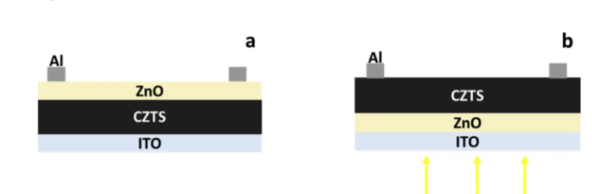
Structures of diodes produced are shown inFig. 2. Morphology, elemental ratios, optical properties and crystalline structures of ZnO1, ZnO2 and CZTS thin films were analysed by Scanning Electron Microscopy (SEM) and Atomic force microscopy (AFM), Energy-dispersive X-ray spectroscopy (SEM-EDX), UV–vis spectrometer and X-ray Powder Diffraction (XRD), respectively. The electrical properties of ITO/a-CZTS/ZnO1/Al diode structure (in dark environment), ITO/ZnO2/a-CZTS/Al and ITO/ZnO2/c-CZTS/Al diode structures (in dark and illumination conditions) are determined by J–V characteristics.
3. Results and discussion
3.1. XRD analysis
As-deposited ZnO thin films were deposited in oxygen ambient gas pressures of 9 × 10⁻²mbar (for ZnO1) and 7 × 10⁻²mbar (for ZnO2) for ITO/a-CZTS/ZnO1/Al and ITO/ZnO2/a-CZTS/Al (and ITO/ZnO2/c-CZTS/Al) diode structures, respectively. Both ZnO1 and ZnO2 thin films have polycrystalline structures according to XRD pattern presented inFig. 3. ZnO1 thin film has a crystallized structure with orientations of 100, 002, 101. A peak appeared with 002 orientation in XRD spectra for both ZnO1&2 thin films is dominant peak and considered to be main peak for both structures [33]. It is very important to indicate that ZnO thin films were produced at room temperature and present a crystalline form obtained without any substrate temperature [34]. Thus, ZnO crystal structure in thin films used as a n-type layer in device is a major contributor to provide charge carrier transfer and collect charges in depletion region. However, it is a fact that ZnO1 thin film is not in a more pronounced crystal structure due to some possible defects in crystal structure. Namely, high oxygen ambient gas pressure slows down ZnO1 particles and ZnO1 particles do not have a good nucleation and orientation because they do not have enough kinetic energies when they reach at substrate [35]. Thus, formed defects can negatively affect performance of device.
Size of main grain in ZnO thin film was calculated by Scherrer equation:
=
D 0.94 / cos (1)
Where D is average size of main grain forming thin film, is the full-width at half-maximum of diffraction main peak, λ is X-ray wavelength and is Bragg diffraction angle in degree [8,11]. Using this equation, main crystalline sizes of ZnO1 and ZnO2 particles in thin film were calculated to be 12.5 nm nm and 21. 53 nm, respectively. In addition, Williamson-Hall (W-H) equation which is more reliable than the Scherrer formula, is also used to calculate the crystalline size. W-H equation is expressed as follows:
= +
cos
D sin
( ) 4 ( ) (2)
Fig. 1. a)Pictures of PLD system, b) plasma of CZTS and c) ZnO species ablated by the laser beam.
Where, is the lattice strain. The crystalline size and lattice strain can be determined depending on the width of the XRD peaks of thin films. Furthermore, in the reciprocal space,
= +
D d
1 4
*2
2 2 *2 (3)
the above equation is used. Where, *= cos / andd*=2sin / [36].
When W*2is plotted depending on d4 *2, the crystalline size of ZnO2 thin film can be calculated from slope of the linear line fit as shown inFig. 4a. The average crystalline size of ZnO2 thin film has been calculated to be 17. 91 nm. As a result, the crystal size found by W-H equation is very close to that obtained by using Scherrer formula. In addition, thicknesses of ZnO1 and ZnO2 thin films were estimated to be 120 nm and 200 nm, respectively.
As-deposited CZTS thin film has an amorphous structure as seen from XRD pattern in Fig. 5since no annealing or no high substrate temperature were applied. Amorphous CZTS thin film indicates that a large number of defects and interfacial states can be found in active layer. Most of these defects can act as a charge trapper and recombination centres limiting performance of diode [37,38]. One of the reasons for amorphous CZTS thin film structure is that it was ablated by a low laser energy and thin films were produced on substrate at room temperature. During the deposition process of CZTS thin film, laser ablation energy was kept low to avoid any damage on ZnO or ITO thin films [39–41]. Therefore, CZTS particles ablated by low laser energy have a low kinetic energy when they reach to substrate, so their diffusion is limited. As a result of nucleation, grain size remains small, and poor crystal structure is formed because it cannot make an harmonious merger for an orientation to form crystal structure [25,26,41]. Therefore, the many defects occurring in a-CZTS act as a trap leading to high electrical resistance of thin film [42,43] which prevents trans-portation of charge carriers and limits accumulation of charges within space charge region of diodes.
CZTS thin film annealed at 375 °C sulfurization temperature that has a polycrystalline structure as shown in XRD pattern inFig. 5. c-CZTS thin film has peaks in 112, 200, 220 and 312 orientations. The highest peak was found in 112 orientation and assumed to be the main peak for c-CZTS thin film in pattern of XRD spectrum. The crystalline structure of c-CZTS thin film reduces the defects in the thin film, thus transportation of the charge carriers into the space charge range is facilitated which results in some increases in the charge collection and photo current. In addition, the main crystalline size of the annealed c-CZTS thin film was calculated to be
Fig. 3. XRD patterns of ZnO1 and ZnO2 thin films.
51.14 nm with Scherrer equation. Furthermore, the crystalline size and micro strain of c-CZTS thin film can be calculated from slope of the linear line fit as shown inFig. 4b, using W-H formula. The average crystalline size of c-CZTS thin film was determined as 50.10 nm. The crystalline sizes calculated with both equations were found to be close and support to each other.
3.2. Morphological analysis
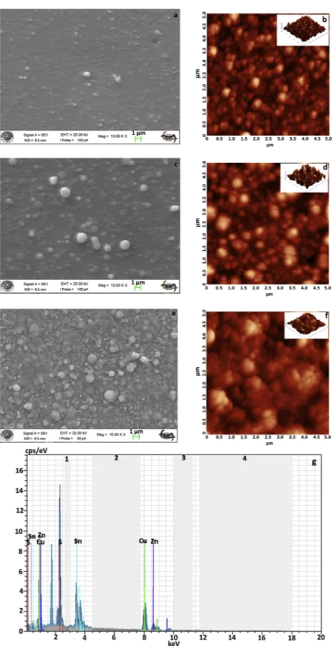
AFM and SEM images of ZnO2 thin film grown in oxygen ambient gas pressure of 7 × 10⁻²mbar are given inFig. 6a and b. Formation of phases of ZnO2 thin film is as follows: Ablated ZnO2 particles react with surrounding oxygen environment, where ambient oxygen pressure were about 7 × 10⁻²mbar, but since gas pressure is kept to be low, ZnO2 atoms can reach at substrate without any significant energy loss. ZnO2 particles coming closer - next to particles located on substrate- have enough energy for diffusion and nucleation. Energetic ZnO2 particles form large islands by joining each other and other particles reached earlier at substrate. In addition, intense ZnO2 particles coming later are added to these islands and then cause particle sizes to grow. Also, energetic ZnO2 particles in low ambient gas pressure diffuse into correct crystallographic regions and initiate crystallization [35]. Therefore, ZnO2 thin film is composed of dense particles, very close to a compact structure, there is a completely inhomogeneous particle distribution in ZnO2 thin film, according to SEM and AFM images given inFig. 6a and b. Average size of particles forming thin film is determined to be between 100 and 150 nm A decrease in number of grain boundaries obtained with an increase in particle size and good crystallization may reduce resistance of ZnO2 thin film [44,45]. Thickness of ZnO2 thin film was measured about 200 nm, which is somewhat higher for use as a buffer layer in solar cells. Roughness of ZnO2 thin film is about 20 nm due to effect of relatively larger particle size [7,22].
SEM and AFM images of a-CZTS thin film as given inFig. 6c and d shows that thin film is made of heterogeneously distributed particles. Particle size was found between 300–500 nm and not considered to be too large. There are two reasons why CZTS na-noparticles forming CZTS thin film are not too large: the first one is that ablation of CZTS particles from a CZTS target was carried out by using low laser pulse energies. The second reason is that CZTS thin film is produced in room temperature and not exposed to any annealing process. Laser ablation energy was kept low enough to avoid any damage on ZnO or ITO thin films during deposition of a-CZTS thin film [39–41]. Therefore, CZTS particles were ablated from target by low laser pulse energies to have particles with low kinetic energies at arrivals on substrate, so their diffusion is limited to nearest particles. Grain size of nanoparticles produced remains small since either CZTS particles arriving at substrate have energies as low as just to reach substrate or the number of particles arriving substrate may also be limited [25,26,35,41–43]. In addition, thin film thickness and roughness values were measured to be 700 nm and 40 nm, respectively, that can result in interface states in joint region of ITO/a-CZTS/ZnO1/Al structure.
TheFig. 6e and f shows SEM and AFM images of c-CZTS thin film annealed at 375 °C sulfurization temperature, respectively. The size of the particles forming c-CZTS thin film were increased due to the annealing process. The number of grain boundaries were decreased by increasing the particle size. Therefore, the traps and defects between grain boundaries are passivated which increases the life-time of photo-excited charge carriers and allows them to accumulate in the depletion range.
3.3. EDX analysis
Atomic ratios of elements in a-CZTS thin film have been obtained from SEM EDX spectrum and are given inTable 1. a-CZTS thin film is Cu-rich and Zn-poor structure [46–48]. Cu/(Zn + Sn) should be unity for CZTS thin films with stoichiometric structure [49]. However, this rate is 1.2 for amorphous CZTS thin film in our study and there is a slight deviation from the stoichiometric ratio [50]. Due to low laser energies, unwanted effects may have occurred during the ablation process of CZTS material consisting of four elements and, therefore, it can be slightly deviated from the stoichiometry of CZTS target structure.
Fig. 6. a) SEM and b) AFM images of ZnO thin film, c) SEM and d) AFM images of a-CZTS thin film, e) SEM and f) AFM images of c-CZTS thin film, g)
3.4. Optical Properties of thin films
Photo transmission of ZnO2 thin film is high according to UV–vis graph inFig. 7a. However, thin film tends to absorb slightly about 560 nm in visible region and about near infra-red and infra-red regions. Thin film of large particles causes transmission of photons to be limited in these regions. In particular, poor photon transmission around 560 nm in visible region can cause some low short circuit current density of ITO/ZnO2/a-CZTS/Al and ITO/ZnO2/c-CZTS/Al diode structures.
Band gap of ZnO thin film was defined by Tauc law:
=
h A h E
( )2 ( g)1/2 (4)
Where A is a constant, Egis band gap of thin film and h is photon energy. Egis acquired by extrapolation of straight line of h( )2vs
h
( )in Tauc plot inFig. 7[51,52]. Band gap of ZnO2 thin film was obtained as 3.37 eV from Tauc graph inFig. 7b. This value is consistent with reported value for ZnO thin film in literature [53,54], which is quite ideal to transmit a large part of photons in a wide band gap from ZnO thin film to active layer.
Absorption spectrum of a-CZTS thin film is given inFig. 8a. Band gap of a-CZTS thin film was obtained to be 1.80 eV from Tauc plot inFig. 8b. This value found in this work is somewhat higher than that of a-CZTS thin film given in literature to be 1–1.5 eV [55,56] that can be attributed to element rate and defects in a-CZTS structure. In addition, low film thickness, small grain size and amorphous structure can cause some increase in band gap [57,58].
The band gap of the crystalline c-CZTS thin film was calculated to be 1.5 eV in this article. c-CZTS thin film has a band gap lower than a-CZTS thin film, which can be attributed to the elimination of many defects in CZTS structure. Furthermore, the band gap of 1.5 eV is the band gap of an ideal CZTS thin film [55,56].
3.5. Electrical characteristics of ITO/a-CZTS/ZnO1/Al diode
According to the J–V characteristics (and logarithmic graph given inset ofFig. 9a) of ITO/a-CZTS/ZnO1/Al structure inFig. 9, the device exhibits rectification behaviour in dark environment. Theory of thermionic emission is used to express this behaviour. Ac-cording to theory, current is expressed by the following equation,
=
I I exp qV nkTo[ ( / ) 1] (5)
Where,Iois saturation current, V is applied voltage, k is Boltzmann constant, q is elementary electric charge, n is ideality factor and T
is absolute temperature.
Table 1
The atomic ratios of elements in a-CZTS thin film.
Cu(%) Zn(%) Sn(%) S(%) Cu/(Zn + Sn) S/metal
30.97 9.21 14.94 44.88 1.2 0.81
Ideality factor n is given by = n q kT dV d lnI( ) (6)
and determined from slope of linear part of semi-logarithmic graph of forward bias J–V characteristics. Semi logarithmic plot of forward bias J–V characteristics of ITO/a-CZTS/ZnO1/Al structure is given inFig. 9b which consists of three different regions expressed by three different slopes. These slopes, m1, m and m2 3were determined to be 0.9, 4.4 and 2.4 from log J-log V curves in I. region, II. region and III. region in the case of forward bias graph inFig. 9b [59–65]. Ideality factors,n n n1, 2, 3, of diode changes depending on these slopes for I., II., III. regions were calculated to be 4,56, 3.86 and 10.43 by using Eq.(6), respectively. Ideality factor of an ideal diode should be 1 < n < 2 [66], but, this varies from 3.86 to 10.43 for ITO/a-CZTS/ZnO1/Al diode structure produced in our present work. Some factors lead to a high ideality factor that shows different values in three regions inFig. 9b : The shunt paths can be formed in diode structure due to pinholes that can form in ZnO1 thin film produced in high oxygen ambient gas pressure leading to a leakage current [59,61]. A leakage current may cause the ideality factor to be large.
In a-CZTS lattice structure, there are defect states causing film to have amorphous structure. In particular, some of defects at interfaces act as a charge trapper [37,46,67]. Therefore, even if a-CZTS thin film behaves as p-type semiconductor [42,50,68], CZTS having amorphous structure, which is one of several factors, to adversely affect its electrical properties [69]. This can cause the sheet resistance of thin film to be high. High sheet resistance of CZTS with amorphous structure results in high series resistivity [12,70,71]. In addition, these trapping centres in a-CZTS can act as recombination points of charge carriers in a quasi-neutral region and negatively affect charge collection as well as good charge separation in joint region [12]. These conditions cause ideality factor to become larger.
Work function of back contact must be higher for ohmic behaviour in p-type semiconductors [72]. 5.25 eV work function of ITO is sufficient to exhibit ohmic behaviour for p-type a-CZTS semiconductor which has 5.5 eV work function [66,73–75]. However, ITO layer, which is a transparent conductive oxide layer, has resistance higher than that of metal layers (such as Mo). Also, no use of any annealing process is one of main factors preventing ITO contact to exhibits ohmic behaviour. These situations cause some high ideality factor [76].
Usage of an oxygen gas in production of ZnO1 thin films on a-CZTS limits high energetic ZnO1 species, ablated from ZnO target material, to enter into a-CZTS thin film. This relatively prevents the formation of deformations in a-CZTS thin film. In addition, production of crystalline ZnO1 thin film at room temperature without using any substrate temperature or annealing temperature during growth of ZnO1 thin film prevents ZnO1 diffusion into a-CZTS layer, and this makes some contributions to the formation of a good p-n junction. This is why, the formation of defects in space charge region is somewhat limited and it may contribute positively to charge collecting behaviour in space charge region.
3.6. Electrical characteristic of ITO/ZnO2/a-CZTS/Al diode
J–V characteristics, logarithmic J–V characteristics and semi-logarithmic forward bias plots of ITO/ZnO2/a-CZTS/Al structure are given for dark environment inFig. 10a, b and c, respectively. Diode structure exhibits an interesting tunnelling diode behaviour
showing a negative differential resistance (NDR), according to forward bias region of logarithmic graph inFig. 10b and c. Tunnelling diode properties [77,78] and NDR of ITO/ZnO2/a-CZTS/Al structure can be attributed to defects in ZnO2 thin film layer. Oxygen ambient gas was used at low pressure about 7 × 10⁻²mbar while ZnO2 thin film was produced on ITO substrate. Therefore, defect states such as zinc interstitial or oxygen vacancies are more likely to occur in growth of ZnO2 thin film. This defect states act as an electron charge trapping region. An increase in number of these defect regions allows ZnO2 thin film to be negatively charged [79–81]. Thus, if charge carrier concentration of ZnO2 thin film can be increased to make heavily doped n-type ZnO semiconductor. ZnO2 thin film has a markedly crystallized structure in direction of (002) in comparison with ZnO1 as seen from XRD pattern in Fig. 3. This results in a doped depletion region cause some tunnelling diode behaviour of ITO/ZnO2/a-CZTS/Al structure.
Band alignment between n-ZnO and p-CZTS becomes mismatched in depletion region [82]. When band gap alignment is es-tablished in interface state between a-CZTS and ZnO2, electrons in conduction band of ZnO2 thin film cannot exceed the built in voltage because 0.05 V applied to device in I. region inFig. 9c that is less than the built in voltage in depletion region. In this case, a small number of electrons tunnel from conduction band of ZnO2 thin film to valance band of a-CZTS thin film layer and this forms a forward bias current density of 6.32 × 10⁻²mA/cm2[83]. When a voltage applied to diode is increased to 0.25 V in II. region, number of electrons passing to valence band of a-CZTS thin film increases, forward bias current density increases and then reaches a maximum current density of 1.81 mA/cm2.When voltage is increased to 0.5 V in III. region (critical voltage region), ITO/ZnO2/a-Fig. 9. J–V characteristics and semi-logarithmic graph in forward bias region of ITO/a-CZTS/ZnO1/Al structure in dark environment is given.
CZTS/Al diode structure displays a negative differential resistance region [77,78,83–86] in III. region of forward bias since an alignment difference can occur between valence band of a-CZTS thin film and conduction band of ZnO2 thin film (a CZTS-ZnO2 bandgap). Trapped electrons in defects in ZnO2 cause a negative charge in tunnelling region that forms an interface barrier in opposed to tunnelling electrons. At present, the diode exhibits NDR behaviour in high resistance region [80,87]. As a result, it was
Fig. 10. a) J–V characteristic, b) logarithmic J–V characteristic and c) semi-logarithmic forward bias plots for ITO/ZnO2/a-CZTS/Al in dark
observed that current density decreases in this region. Even if inconsistent alignment occurs between bands, a few electrons in conduction band of ZnO2 tunnels to valence band of a-CZTS, since bands are still overlapping with each other. When voltage reaches to 0.5 V, current density drops down to 1.26 × 10⁻¹mA/cm2. When voltage at IV. region is increased, current density starts to increase. Now, ITO/ZnO2/a-CZTS/Al structure behaves like a normal p-n junction diode in IV. region. Since voltage applied to this region is greater than the built-in voltage in depletion region, forward current gradually increases [77].
J–V characteristics of ITO/ZnO2/a-CZTS/Al diode structure under illumination conditions, given inFig. 11, indicate that the diode presents some photo-electric properties. Electrical parameters of the diode are given inTable 2.
Since high substrate and annealing temperature in production of CZTS thin film were not used, it can be said that no cracks in a-CZTS thin film were observed and penetration of a-a-CZTS thin film and ZnO2 thin film into each other were not observed. Thickness of ZnO2 thin film as a buffer layer was measured to be quite high. However, as ZnO2 thin film thickness increases, number of voids within film decreases and film becomes a continuous structure and, therefore, a better crystallization occurs in ZnO2 thin film. ITO layer, which is a transparent conductive oxide, is an ideal electrode for solar cells because it transmits most of incoming photons and collects charges on itself. In addition, although CZTS is an amorphous structure, a small number of charge carriers to be formed in a-CZTS thin film can cause the charge accumulation in the joint region [88]. All of these factors have provided that ITO/ZnO2/a-CZTS/ Al exhibits photo-electric effects.
The Jscvalue of diode is determined to be 0.051 mA/cm2and was commented to be very low. Low current value can be attributed to many reasons depending on a-CZTS thin film. Since thickness of a-CZTS thin film is low, this means that absorption rate of incident photon is lower in active layer. Therefore, number of photo-excited charge carriers is small and charge accumulation in space charge region is low, and leads to a low Jscvalue. In addition, photons with energy above band gap of a-CZTS thin film can excite charge carriers to active layer. Photons coming to active layer with some energy below a-CZTS thin film band gap cannot be absorbed [89]. However, since band gap of active layer is large, it reduces photo-excitation of electrons in active layer and, therefore, current density is limited [90]. Some of defects ingrain boundaries and interfacial states in a-CZTS thin film have played a key role as a re-combination centre. Minority charge carriers, that are formed as a result of photo-excitation, could be small in amorphous CZTS thin film [88], and are destroyed in these trap centres. Amorphous structure of CZTS thin film enhances a series resistance that causes Jsc to be small [88,91]. Furthermore, number of grain boundaries is high since a-CZTS thin film consists of small grain sizes. Minority charge carriers can recombine in traps within these particle boundaries that causes a low Jsc.
Since ZnO2 thin film is composed of large particles and thickness of thin film is 200 nm, ZnO2 thin film performs a certain amount of photon absorption at a wavelength of 560 nm in visible region and between NIR and IR region, as shown in UV–vis spectrum of Fig. 7a. Therefore, photons absorbed in this region are limited to be transferred into a-CZTS structure. This has a negative effect on photo current formation in a-CZTS and, therefore, on short circuit current density. Also, the shunt pathways can be formed inside the diode due to the possibility of the formation of pinholes in ZnO2 and a-CZTS thin film, which lead to the low short circuit current density.
Vocvalue and fill factor have been determined to be 600 mV and 0.64, respectively. These values are quite high despite Jscbeing low. The large band gap of a-CZTS thin film was found to be 1.80 eV and causes a high open circuit voltage [92]. Vochas a high value due to a high band gap (Eqg V )oc, as it is directly proportional to separation between quasi Fermi levels of p- and n-types [89,93–97].
CZTS thin film, grown as a compact structure on ZnO2 which has a low roughness value produced by PLD, leads to a high Voc[98]. According to literature [99–101], increases in Vocand FF values are based on doping density in depletion region when Jscdecreases. Excess of doping rate and high charge density in depletion region due to ZnO2 thin film may cause the width of the depletion region to become narrower [77]. A narrowing in depletion region in p-CZTS/n-ZnO can also lead to a low Jsc[13,98,102–105]. In addition, it is assumed that ITO/ZnO2/a-CZTS/Al structure exhibits tunnelling diode characteristics in dark environment and tunnelling diode
Fig. 11. J–V plot of ITO/ZnO2/a-CZTS/Al under illumination condition.
Table 2
The electrical parameters of ITO/ZnO2/a-CZTS/Al diode structure.
Jsc Voc FF η
has a very narrow depletion region [77]. Therefore, a narrow depletion region causes high Vocand low Jsc[100,106]. Since ZnO2 thin film has wide band gap (3.37 eV) as a buffer layer and can create high built-in potential in depletion region, Vocincreases [12].
Reasons for power conversion efficiency being low are generally expressed as: i) as-deposited a-CZTS thin film is in amorphous structure and there are some defects in it, these defects acts as a recombination center for minority charge carriers [88], ii) Since annealing temperature is not applied, contacts may not exhibit ohmic behaviour, iii) as indicated above, insufficient charge collection in space charge region may be observed, iv) diode exhibits tunnelling diode characteristics, v) due to low thickness of a-CZTS thin film, insufficient photon absorption limits photo-current formation, vi) loss of photons due to high thickness of ZnO2 thin film. These conditions limit power conversion efficiency where short circuit current density is low. However, high values of Vocand FF prevents η value to be much lower. As a result, elimination of such problems, that may cause short circuit current density to be low and contribute to power conversion efficiency.
3.7. Electrical characteristic of ITO/ZnO2/c-CZTS/Al diode
According to the J–V characteristics (and logarithmic graph given inset ofFig. 12a) of the ITO/ZnO2/c-CZTS/Al structure in Fig. 12, device exhibits some weak rectification behaviour in dark environment. The ideality factor and the slope were calculated to be 6.96 and 1.1 from semi logarithmic plot of forward bias J–V characteristics of ITO/ZnO2/c-CZTS/Al structure given inFig. 12b, respectively. The ideality factor is found to be higher for ITO/ZnO2/c-CZTS/Al diode structure. An important point here, the charge collection in the depilation region may be adversely affected due to the possibility of diffusing CZTS thin film, annealed at 375 °C sulfurization temperature, into the ZnO2 thin film. The defect structure and trap sites formed in the depilation region lead to a leakage of carriers in depilation region. These conditions can cause the ideality factor to be large [107].
Fig. 12. J–V characteristics and semi-logarithmic graph in forward bias region of ITO/ZnO2/c-CZTS/Al structure in dark environment is given.
The logarithmic J–V characteristic of ITO/ZnO2/c-CZTS/Al diode structure under illumination conditions, given inFig. 13, in-dicates that the diode exhibits photo-electric behaviour. Electrical parameters of the diode are presented inTable 3.
Electrical parameters of Voc, Jsc, FF and η are found to be 20 mV, 3.6 mA/cm2, 0.65, and 0.06%, respectively, according to the logarithmic J–V characteristic shown inFig. 13and given in Table 3. After CZTS thin film was annealed, Jscvalue of the diode significantly increased while Vocvalue decreased significantly in comparison. The power conversion efficiency of ITO/ZnO2/c-CZTS/ Al diode structure is found to be three times higher than that of ITO/ZnO2/a-CZTS/Al diode structure. The crystalline structure of the annealed CZTS thin film have significantly contributed to photo electricity property of the diode. The defect structures and the trapped regions in the crystalline CZTS thin film is reduced and recombination points are passivated compared to a-CZTS thin film. Thus, more photo-excited charge carriers have been formed within c-CZTS thin film and then Jscvalue has been increased.
After 375 °C sulfurization annealing process, the band gap of CZTS thin film was decreased from 1.80 eV to 1.50 eV. This decrease in the band gap is very effective to reduce Vocvalue [92,95]. The built in potential reduces as the band gap of CZTS thin film reduces [108]. The leakage current in the depilation region increases as the built-in potential decreases, and then Vocvalue decreases too [109,110]. In addition, CZTS thin film annealed at 375 °C sulfurization temperature is likely to embedded and diffuse into ZnO2 thin film causing both defect structures in deplation region and the formation of non-ideal deplation region. The defects and re-combi-nation points can be formed in deplation region lead to leakage current in the deplation region [111]. Therefore, this also result in reduction of Vocvalue. As a result, Jscsignificantly increases and Vocsignificantly decreases due to that in the other diode. So, it has been noticed that power conversion efficiency was threefold increased.
4. Conclisions
In this study, ITO/a-CZTS/ZnO1/Al and ITO/ZnO2/a-CZTS/Al diode structures were produced at room temperature while ITO/ ZnO2/c-CZTS/Al diode structure produced with CZTS thin film annealed at 375 °C sulfurization temparature, all diode structures were produced by PLD system. ITO/a-CZTS/ZnO1/Al diode exhibits normal diode behaviour while ITO/ZnO2/a-CZST/Al shows tunnelling diode behaviour in dark environment. Three different ideality factors have been determined in forward bias region of ITO/ a-CZTS/ZnO1/Al structure. Tunnelling behaviour of ITO/ZnO2/a-CZTS/Al diode structure is based on oxygen vacancies and inter-stitial Zn defect sites in ZnO thin film. Since these defects can create doping effects within ZnO2 thin film, they can create a doping and narrow depletion region. It is thought that these conditions cause diode to have tunnelling behaviour. ITO/ZnO2/a-CZTS/Al diode structure exhibits photoelectric behaviour in illumination conditions. Electrical characteristics of Jsc, Voc, FF and η for a diode under illumination conditions were obtained to be 0.051 mA/cm2, 600 mV, 0.64, 0.02%, respectively. Low short circuit current density and higher open circuit voltage may be attributed to a high band gap of a-CZTS thin film and narrow depletion region. In particular, low short-circuit current is attributed to insufficient charge collection in space charge region and defects as recombination centers in a-CZTS thin film having amorphous structure.
CZTS thin film annealed at 375 °C sulfurization temperature has a crystalline structure. Electrical parameters of Jsc, Voc, FF and η for ITO/ZnO2/c-CZTS/Al diode formed with c-CZTS and ZnO2 thin films under illumination conditions were determined to be 3.6 mA/cm2, 20 mV, 0.65 and 0.06%, respectively.
The increase in Jscvalue can be attributed to some passivation of defect structures and traps (re-combination) in CZTS thin film. However, the reduction of the band gap of CZTS thin film may cause some reduction in Vocvalue. Furthermore, CZTS thin film annealed at 375 °C sulfurization temperature may have been embedded and diffused into ZnO2 thin film. Thus, there may be some defects and recombination points in the depilation region leading to leakage current and hence, the decrease in Vocvalue.
The efficiency of ITO/ZnO2/c-CZTS/Al diode structure is increased three times compared to the efficiency of ITO/ZnO2/a-CZTS/ Al diode structure by annealing of CZTS thin film. However, the efficiency of both diodes is still low. In order to overcome this problem, CZTS must be produced at appropriate substrate temperature, or CZTS thin film should be annealed at more appropriate sulfurization temperature with the amount of suitable sulphur powder, in order not to cause any defect in depletion region and the thin films. In addition, ZnO thin film can also be annealed at an appropriate temperature for ideal surface tension. It can be said that the diffusion and embedding of CZTS thin film into ZnO and then the formation of defects and leakage currents in the depilation region can be prevented. As a result, the power conversion efficiency can be enhansed by increasing Vocand Jscvalues.
Acknowledgements
Authors kindly would like to thank,Scientific and Technical Research Council of Turkey (TUBITAK) for financial support via Grant No. 1649B031503748, Selçuk University, High Technology Research and Application Centre for supplying with Infrastructure and budget via 15301020 and 18401178 projects.
Table 3
The electrical parameters of ITO/ZnO2/c-CZTS/Al diode structure.
Jsc Voc FF η
[11] R. Khandelwal, et al., Effects of deposition temperature on the structural and morphological properties of thin ZnO films fabricated by pulsed laser deposition, Opt. Laser Technol. 40 (2) (2008) 247–251.
[12] M.T. Htay, et al., A cadmium-free Cu2ZnSnS4/ZnO hetrojunction solar cell prepared by practicable processes, J. Appl. Phys. 50 (3R) (2011) 032301. [13] S.K. Silvi, M.I.B. Chowdhury, Modeling of JV characteristics of CZTS based thin film solar cells including voltage and space dependent electric field in the
absorber layer, Development in the in Renewable Energy Technology (ICDRET), 2016 4th International Conference on the (2016) 1–4.
[14] S.K. Swami, A. Kumar, V. Dutta, Deposition of kesterite Cu2ZnSnS4 (CZTS) thin films by spin coating technique for solar cell application, Energy Procedia 33 (2013) 198–202.
[15] S. Vanalakar, et al., A review on pulsed laser deposited CZTS thin films for solar cell applications, J. Alloys Compd. 619 (2015) 109–121. [16] Y. Curé, S. Pouget, V. Reita, H. Boukari, Cu2ZnSnSe4 thin films grown by molecular beam epitaxy, Scr. Mater. 130 (2017) 200–204. [17] K. Ramasamy, M.A. Malik, P. O’Brien, The chemical vapor deposition of Cu 2 ZnSnS 4 thin films, Chem. Sci. 2 (6) (2011) 1170–1172.
[18] Z. Chen, K. Shum, T. Salagaj, W. Zhang, K. Strobl, ZnO thin films synthesized by chemical vapor deposition, Applications and Technology Conference (LISAT), 2010 Long Island Systems (2010) 1–6.
[19] L. Xu, X. Li, Y. Chen, F. Xu, Structural and optical properties of ZnO thin films prepared by sol–gel method with different thickness, Appl. Surf. Sci. 257 (9) (2011) 4031–4037.
[20] A. Moholkar, et al., Development of CZTS thin films solar cells by pulsed laser deposition: influence of pulse repetition rate, Sol. Energy 85 (7) (2011)
1354–1363.
[21] A. Moholkar, et al., Synthesis and characterization of Cu2ZnSnS4 thin films grown by PLD: solar cells, J. Alloys. Compd. 509 (27) (2011) 7439–7446. [22] A.O. Dikovska, P. Atanasov, C. Vasilev, I. Dimitrov, T. Stoyanchov, Thin ZnO films produced by pulsed laser deposition, J. Optoelectron. Adv. Mater. 7 (2005)
1329–1334.
[23] A.C. Cazzaniga, J. Schou, N. Pryds, P.M. Petersen, Fabrication of Thin Film CZTS Solar Cells With Pulsed Laser Deposition, Technical University of Denmark (DTU), 2016.
[24] C.M. Ghimbeu, F. Sima, R. Ostaci, G. Socol, I. Mihailescu, C. Vix-Guterl, Crystalline vanadium nitride ultra-thin films obtained at room temperature by pulsed laser deposition, Surf. Coat. Technol. 211 (2012) 158–162.
[25] B. Thestrup, J. Schou, Transparent conducting AZO and ITO films produced by pulsed laser ablation at 355 nm, Appl. Phys. A 69 (1) (1999) S807–S810. [26] Ş. Tozan, Fabrication of YBCO Thin Flims by Pulsed Laser Deposiyion Technique and Their Charcterization, İzmir Institute of Technology, 2010. [27] I.W. Boyd, Thin film growth by pulsed laser deposition, Laser and Ion Beam Modification of Materials, Elsevier, 1994, pp. 319–326.
[28] J.M. Lackner, W. Waldhauser, T. Schöberl, Film growth phenomena in high-energetic room temperature pulsed laser deposition on polymer surfaces, Surf. Coat. Technol. 201 (7) (2006) 4037–4039.
[29] D.B. Chrisey, G.K. Hubler, Pulsed Laser Deposition of Thin Film, John Wiley & Sons, Inc., New York, 1994.
[30] A. El Kissani, et al., Structural, optical, and electrical properties of Kësterite/Zinc oxide heterostructures, Spectrosc. Lett. 47 (5) (2014) 387–391. [31] K. Yang, M. Ichimura, Fabrication of Cu–Zn–Sn–S–O thin films by the electrochemical deposition method and application to heterojunction cells, Int. J.
Photoenergy 2012 (2012).
[32] H.S. Kılıç, H. Durmus, Yeni bir puls laser depozisyon (PLD) sistemi tasarımı, üretimi ve uygulamaları, (2016). [33] L. Znaidi, et al., AZO thin films by sol-gel process for integrated optics, Coatings 3 (3) (2013) 126–139.
[34] M.-j. Jin, J. Jo, G.P. Neupane, J. Kim, K.-S. An, J.-W. Yoo, Tuning of undoped ZnO thin film via plasma enhanced atomic layer deposition and its application for an inverted polymer solar cell, AIP Adv. 3 (10) (2013) 102114.
[35] R. Kumar, G. Kumar, A. Umar, Pulse laser deposited nanostructured ZnO thin films: a review, J. Nanosci. Nanotechnol. 14 (2) (2014) 1911–1930. [36] A. Weibel, R. Bouchet, F. Boulc’, P. Knauth, The big problem of small particles: a comparison of methods for determination of particle size in nanocrystalline
anatase powders, Chem. Mater. 17 (9) (2005) 2378–2385.
[37] L. Yin, G. Cheng, Y. Feng, Z. Li, C. Yang, X. Xiao, Limitation factors for the performance of kesterite Cu 2 ZnSnS 4 thin film solar cells studied by defect characterization, RSC Adv. 5 (50) (2015) 40369–40374.
[38] E. Lund, Defect Characterization and Phase Analyses of Copper Zinc Tin sulfide/selenide, The University of Utah, 2014. [39] wikipedia, Pulsed Laser Deposition, 03.09 (2018).
[40] A. Voevodin, M. Donley, Preparation of amorphous diamond-like carbon by pulsed laser deposition: a critical review, Surf. Coat. Technol. 82 (3) (1996) 199–213.
[41] J. Gottmann, E. Kreutz, Controlling crystal quality and orientation of pulsed-laser-deposited BaTiO3 thin films by the kinetic energy of the film-forming particles, Appl. Phys. A 70 (3) (2000) 275–281.
[42] M. Rabeh, R. Touatti, M. Kanzari, Substrate temperature effects on structural optical and electrical properties of vacuum evaporated Cu2ZnSnS4 thin films, Int. J. Eng. Pract. Res. (2013).
[43] M. Islam, et al., Properties of low temperature vacuum annealed CZTS thin films deposited on polymer substrate, Chalcogenide Letters 11 (5) (2014) 233–239. [44] C. Periasamy, R. Prakash, P. Chakrabarti, Effect of post annealing on structural and optical properties of ZnO thin films deposited by vacuum coating technique,
J. Mater. Sci. Mater. Electron. 21 (3) (2010) 309–315.
[45] H. Mahdhi, Z. Ben Ayadi, L. El Mir, K. Djessas, S. Alaya, Elaboration and characterization of Ca doped ZnO films prepared by rf-magnetron sputtering at room temperature, Sens. Lett. 9 (6) (2011) 2150–2153.
[46] M. Kumar, A. Dubey, N. Adhikari, S. Venkatesan, Q. Qiao, Strategic review of secondary phases, defects and defect-complexes in kesterite CZTS–Se solar cells, Energy Environ. Sci. 8 (11) (2015) 3134–3159.
[47] S. Chen, X. Gong, A. Walsh, S.-H. Wei, Defect physics of the kesterite thin-film solar cell absorber Cu 2 ZnSnS 4, Appl. Phys. Lett. 96 (2) (2010) 021902. [48] S. Chen, A. Walsh, X.G. Gong, S.H. Wei, Classification of lattice defects in the kesterite Cu2ZnSnS4 and Cu2ZnSnSe4 earth‐abundant solar cell absorbers, Adv.
Mater. 25 (11) (2013) 1522–1539.
[50] M. Farinella, P. Livreri, S. Piazza, C. Sunseri, R. Inguanta, One-Step Electrodeposition of CZTS for Solar Cell Absorber Layer, Electroplating of Nanostructures: InTech, 2015.
[51] E. Keskenler, et al., Growth and characterization of Ag/n-ZnO/p-Si/Al heterojunction diode by sol–gel spin technique, J. Alloys. Compd. 550 (2013) 129–132. [52] F. Bedia, A. Bedia, B. Benyoucef, Electrical properties of ZnO/p-Si heterojunction for solar cell application, Int. J. Mater. Eng. 3 (4) (2013) 59–65. [53] N. Hassan, M. Hashim, Structural and optical properties of ZnO thin film prepared by oxidation of Zn metal powders, Sains Malays. 42 (2) (2013) 193–196. [54] E. Muchuweni, T. Sathiaraj, H. Nyakotyo, Synthesis and characterization of zinc oxide thin films for optoelectronic applications, Heliyon 3 (4) (2017) e00285. [55] S. Vanalakar, et al., Effect of post-annealing atmosphere on the grain-size and surface morphological properties of pulsed laser deposited CZTS thin films,
Ceram. Int. 40 (9) (2014) 15097–15103.
[56] C. Malerba, et al., CZTS stoichiometry effects on the band gap energy, J. Alloys. Compd. 582 (2014) 528–534. [57] Shodhganga, "Effect of thickness on the properties of CZTS thin films," Effect of thickness on CZTS thin films.
[58] M. Rao, S.S. Basha, Structural and electrical properties of CZTS thin films by electrodeposition, Results Phys. 9 (2018) 996–1006.
[59] P. Yadav, K. Pandey, B. Tripathi, M. Kumar, Investigation of interface limited charge extraction and recombination in polycrystalline silicon solar cell: using DC and AC characterization techniques, Sol. Energy 116 (2015) 293–302.
[60] P. Liao, X. Zhao, G. Li, Y. Shen, M. Wang, A new method for fitting current–voltage curves of planar heterojunction perovskite solar cells, Nano-micro Lett. 10 (1) (2018) 5.
[61] J.D. Servaites, M.A. Ratner, T.J. Marks, Organic solar cells: a new look at traditional models, Energy Environ. Sci. 4 (11) (2011) 4410–4422. [62] X. Shen, D. Zhao, Z. Liu, Z. Hu, H. Yang, J. Liang, Space-charge-limited currents in GaN schottky diodes, Solid. Electron. 49 (5) (2005) 847–852. [63] V. Janardhanam, I. Jyothi, J.-H. Lee, J.-Y. Kim, V.R. Reddy, C.-J. Choi, Electrical properties and carrier transport mechanism of Au/n-GaN schottky contact
modified using a copper pthalocyanine (CuPc) interlayer, Mater. Trans. 55 (5) (2014) 758–762.
[64] D. Shi, et al., Low trap-state density and long carrier diffusion in organolead trihalide perovskite single crystals, Science 347 (6221) (2015) 519–522. [65] Ş. Aydoğan, K. Çınar, H. Asıl, C. Coşkun, A. Türüt, Electrical characterization of Au/n-ZnO Schottky contacts on n-Si, J. Alloys. Compd. 476 (1-2) (2009)
913–918.
[66] M. Patel, I. Mukhopadhyay, A. Ray, Study of the junction and carrier lifetime properties of a spray-deposited CZTS thin-film solar cell, Semicond. Sci. Technol. 28 (5) (2013) 055001.
[67] S. Kim, J.-S. Park, A. Walsh, Identification of killer defects in kesterite thin-film solar cells, ACS Energy Lett. 3 (2) (2018) 496–500. [68] H. Nguyen Thi, Fabrication of Cu2ZnSnS4 Semiconductor Thin Films Using a Spray Pyrolysis Method for Photovoltaic Applications, (2018). [69] A. Noble, A. Zakari, Characterization of CZTS absorbent material prepared by field-assisted spray pyrolysis, Am. J. Mater. Sci. 4 (3) (2014) 127–132. [70] D. Bhattacharya, A. Mansingh, P. Swarup, Dependence of series resistance on operating current in pn junction solar cells, Sol. Cells 18 (2) (1986) 153–162. [71] S.R. Kodigala, Thin Film Solar Cells From Earth Abundant Materials: Growth and Characterization of Cu2 (ZnSn)(SSe) 4 Thin Films and Their Solar Cells,
Newnes, 2013.
[72] K.K. Kurhade, Electrical Characterization of GaN and SiC Schottky Diodes and Non Mechanical Beam Steering Using Liquid Crystals, (2015).
[73] J.-S. Kim, J.-K. Kang, D.-K. Hwang, High efficiency bifacial Cu2ZnSnSe4 thin-film solar cells on transparent conducting oxide glass substrates, APL Mater. 4 (9) (2016) 096101.
[74] U. Saha, M.K. Alam, Boosting the efficiency of single junction kesterite solar cell using Ag mixed Cu 2 ZnSnS 4 active layer, RSC Adv. 8 (9) (2018) 4905–4913. [75] J. Tao, et al., Synthesis and characterization of Cu 2 ZnSnS 4 thin films by the sulfurization of co-electrodeposited Cu–Zn–Sn–S precursor layers for solar cell
applications, RSC Adv. 4 (46) (2014) 23977–23984.
[76] M. Denhoff, N. Drolet, The effect of the front contact sheet resistance on solar cell performance, Sol. Energy Mater. Sol. Cells 93 (9) (2009) 1499–1506. [77] T. Diode. (2018).
[78] T. Diode, Tunnel Diode, 03.09 (2018).
[79] M.-Y. Chuang, et al., Negative differential resistance behavior and memory effect in laterally bridged ZnO nanorods grown by hydrothermal method, ACS Appl. Mater. Interfaces 6 (8) (2014) 5432–5438.
[80] N. Roy, A. Chowdhury, A. Roy, Observation of negative differential resistance and electrical bi-stability in chemically synthesized ZnO nanorods, J. Appl. Phys. 115 (22) (2014) 223502.
[81] Y. Fang, J. Li, Y. Chen, W. Zhang, C. Jia, Magnetic field-induced bipolar resistive switching and negative differential resistance in (110) SrTiO3: Nb/ZnO heterojunctions, Physica B Condens. Matter 521 (2017) 69–72.
[82] H. Li, et al., Epitaxial growth of ZnO nanorods on diamond and negative differential resistance of n-ZnO nanorod/p-diamond heterojunction, Appl. Surf. Sci. 280 (2013) 201–206.
[83] X. Zeng, G. Otnes, M. Heurlin, R.T. Mourão, M.T. Borgström, InP/GaInP nanowire tunnel diodes, Nano Res. 11 (5) (2018) 2523–2531.
[84] W.F. Mohammed, O. Daoud, M. Al-Tikriti, Power conversion enhancement of CdS/CdTe solar cell interconnected with tunnel diode, Circuits Syst. 3 (03) (2012) 230.
[85] H. Schmid, C. Bessire, M.T. Björk, A. Schenk, H. Riel, Silicon nanowire Esaki diodes, Nano Lett. 12 (2) (2012) 699–703.
[86] S. Rathi, S.K. Gupta, C.M.S. Negi, A. Singh, Negative differential resistance in heterojunction polymeric films, Superlattices Microstruct. 114 (2018) 15–22. [87] P. Chen, X. Ma, D. Li, Y. Zhang, D. Yang, Electrically pumped ultraviolet random lasing from ZnO-based metal-insulator-semiconductor devices: dependence on
carrier transport, Opt. Express 17 (6) (2009) 4712–4717.
[88] Z. Shi, A.H. Jayatissa, One-pot hydrothermal synthesis and fabrication of kesterite Cu2ZnSn (S, Se) 4 thin films, Prog. Nat. Sci. 27 (5) (2017) 550–555. [89] A. Polman, H.A. Atwater, Photonic design principles for ultrahigh-efficiency photovoltaics, Nat. Mater. 11 (3) (2012) 174.
[90] PVeducation.org, Short-Circuit Current, (2018).
[91] M. Kurokawa, K. Tanaka, K. Moriya, H. Uchiki, Fabrication of three-dimensional-structure solar cell with Cu2ZnSnS4, J. Appl. Phys. 51 (10S) (2012) 10NC33. [92] PVeducation.org. (2018).https://www.pveducation.org/pvcdrom/open-circuit-voltage.
[93] B. Qi, J. Wang, Open-circuit voltage in organic solar cells, J. Mater. Chem. 22 (46) (2012) 24315–24325.
[94] J. Yan, G. Luo, B. Xiao, H. Wu, Z. He, Y. Cao, Origin of high fill factor in polymer solar cells from semiconducting polymer with moderate charge carrier mobility, Org. Electron. 24 (2015) 125–130.
[95] T. Tayagaki, Y. Hoshi, N. Usami, Investigation of the open-circuit voltage in solar cells doped with quantum dots, Sci. Rep. 3 (2013) 2703. [96] A. Polizzotti, I.L. Repins, R. Noufi, S.-H. Wei, D.B. Mitzi, The state and future prospects of kesterite photovoltaics, Energy Environ. Sci. 6 (11) (2013)
3171–3182.
[97] S. Bourdais, et al., Is the Cu/Zn disorder the main culprit for the voltage deficit in kesterite solar cells? Adv. Energy Mater. 6 (12) (2016) 1502276. [98] M. Yang, et al., The Cu2ZnSnS4 solar cell with high open circuit voltage, Physica B Condens. Matter 509 (2017) 50–54.
[99] Y. Peng, L. Zhang, T.L. Andrew, High open-circuit voltage, high fill factor single-junction organic solar cells, Appl. Phys. Lett. 105 (8) (2014) p. 135_1. [100] Y. Zhao, et al., Effect of doping on the short-circuit current and open-circuit voltage of polymer solar cells, J. Appl. Phys. 116 (15) (2014) 154506. [101] Y.J. Hofstetter, P.E. Hopkinson, A.A. Bakulin, Y. Vaynzof, Simultaneous enhancement in open circuit voltage and short circuit current of hybrid
organic–i-norganic photovoltaics by iorganic–i-norganic interfacial modification, J. Mater. Chem. C 4 (5) (2016) 1111–1116.
[102] J. Li, et al., 10% Efficiency Cu2ZnSn (S, Se) 4 thin film solar cells fabricated by magnetron sputtering with enlarged depletion region width, Sol. Energy Mater. Sol. Cells 149 (2016) 242–249.
[103] J. Li, et al., Tailoring the defects and carrier density for beyond 10% efficient CZTSe thin film solar cells, Sol. Energy Mater. Sol. Cells 159 (2017) 447–455. [104] J. Zhu, et al., Enhancement of open-circuit voltage and the fill factor in CdTe nanocrystal solar cells by using interface materials, Nanotechnology 25 (36)
(2014) 365203.
[105] J. Zhang, Y.-G. Jung, Advanced Ceramic and Metallic Coating and Thin Film Materials for Energy and Environmental Applications, Springer, 2018. [106] S. Tajima, T. Itoh, H. Hazama, K. Ohishi, R. Asahi, Improvement of the open-circuit voltage of Cu2ZnSnS4 solar cells using a two-layer structure, Appl. Phys.