PREPARATION AND CHARACTERIZATION
OF POLYMER COMPOSITES CONTAINING
GOLD NANOPARTICLES
a dissertation submitted to
the department of chemistry
and the graduate school of engineering and science
of bilkent university
in partial fulfillment of the requirements
for the degree of
doctor of philosophy
By
Eda Yılmaz
September, 2011
I certify that I have read this thesis and that in my opinion it is fully adequate, in scope and in quality, as a dissertation for the degree of doctor of philosophy.
Prof. Dr. S¸efik S¨uzer (Advisor)
I certify that I have read this thesis and that in my opinion it is fully adequate, in scope and in quality, as a dissertation for the degree of doctor of philosophy.
Prof. Dr. Erdal Bayramlı
I certify that I have read this thesis and that in my opinion it is fully adequate, in scope and in quality, as a dissertation for the degree of doctor of philosophy.
I certify that I have read this thesis and that in my opinion it is fully adequate, in scope and in quality, as a dissertation for the degree of doctor of philosophy.
Assist. Prof. Dr. Erman Beng¨u
I certify that I have read this thesis and that in my opinion it is fully adequate, in scope and in quality, as a dissertation for the degree of doctor of philosophy.
Assist. Prof. Dr. Co¸skun Kocaba¸s
Approved for the Institute of Engineering and Science:
Prof. Dr. Levent Onural Director of the Institute
ABSTRACT
PREPARATION AND CHARACTERIZATION OF POLYMER COMPOSITES CONTAINING GOLD NANOPARTICLES
EDA YILMAZ
Ph.D. in Chemistry
Supervisor: Prof. Dr. Şefik Süzer September, 2011
In this study, light-assisted synthesis of gold nanoparticles in polymer films is demonstrated and characterization of gold nanoparticle-polymer composites using various techniques is shown. There are various methods introduced for the synthesis of gold nanoparticles in solution and their integration to the polymer films afterwards. However, synthesizing gold nanoparticles directly inside the polymer matrix is more advantageous for the production of polymer-nanoparticle composites.
An advantage of synthesizing gold nanoparticles within polymer films is the opportunity of photo-patterning. Films having patterns made of regions with and without gold nanoparticles can be produced, using masks designed to cut off the radiation at desired places. Such patterned films were investigated with scanning electron microscope (SEM) and dark regions between irradiated regions and masked regions were observed. These dark regions are shown to be “ion depleted regions”, where gold ions diffuse through irradiated regions during the irradiation. These regions of about 10 m width, suggests a very large distance for gold ions to diffuse through a rigid matrix like Poly(methyl methacrylate)(PMMA), which is very interesting. Supporting evidence for the existence of these regions was obtained from fluorescence studies with Rhodamine 6G molecule and x-ray electron spectroscopy (XPS). The observations made through the formation of ion depleted regions can be used to estimate the diffusion constant of gold ions inside the PMMA matrix. Also the presence of ion depleted regions indicate the stability of photo-patterns created on the polymer film against
smearing during light exposure after the production, by setting an upper limit to the critical feature size.
During the characterization of gold nanoparticle-polymer composites, the electrical properties of PMMA with and without gold nanoparticles were investigated using charge resolved XPS, while applying external bias to the films with and without gold nanoparticles to probe the charging properties of the films. An enhancement of conductivity of PMMA films containing gold nanoparticles was observed using this technique. Additionally charge resolved XPS technique was also used to determine the charge storage characteristics of the polymer surfaces, which is important for the identification of charging mechanisms during contact and other electrification processes. It was shown that the PMMA surface is very susceptible to negative charging and even native negative charges on the PMMA surface can be observed prior to any treatment. Also when the surface is charged carbon and oxygen atoms of the carbonyl and methoxy groups of PMMA were observed to behave differently from the backbone of the polymer, which shows the chemical specificity of the charge accumulating spots on the surface.
Keywords: Gold nanoparticle, PMMA, XPS, Charge resolved XPS, Photo-patterning, Ion depleted region, Contact electrification
ÖZET
ALTIN NANOPARÇACIKLARI İÇEREN POLİMER KOMPOSİTLERİNİN HAZIRLANMASI VE KARAKTERİZASYONU
EDA YILMAZ
Danışman: Prof. Dr. Şefik Süzer Eylül, 2011
Bu çalışmada altın nanoparçacıklarının polimer filmleri içerisinde ışık yardımıyla sentezlenmesi ve çeşitli teknikler kullanılarak altın nanoparçacığı-polimer kompositlerinin karakterizasyonu gösterilmektedir. Altın nanoparçacıklarının çözelti fazında sentezini ve sonradan polimer filmlerine bütünleştirilmesini gösteren başka çalışmalarda mevcuttur. Fakat bu uygulamalara nazaran altın nanoparçacıklarının polimer filmleri içerisinde sentezlenmesi, polimer-nanoparçacık kompositlerinin üretimi açısından daha basit ve avantajlıdır.
Altın nanoparçacıklarının polimer filmleri içinde sentezlenmesinin bir avantajı, bu tekniğin ışıkla desenleme uygulamalarına imkan sağlamasıdır. Bu yöntemle UV ışığını istenen bölgelerde kesen maskeler kullanılarak, polimer içinde altın nanoparçacığı içeren ve içermeyen bölgelerden oluşan desenler oluşturulabilir. Bu şekilde oluşturulan desenli filmlerin taramalı elektron mikroskobu ile incelenmesi sırasında, maskelenmiş ve radyasyona maruz bırakılmış bölgeler arasında mikroskopta koyu gözüken bölgeler tespit edilmiştir. Bu koyu bölgeler “İyondan arındırılmış bölgeler” olarak adlandırılmış olup oluşumları sırasında altın iyonlarının radyasyona maruz bırakılmış bölgelere doğru hareket ettiği düşünülmektedir. İyonların bu bölgeleri oluştururken katı bir polimer filmi içerisinde 10 µm gibi uzun bir mesafe kat etmesi ilgi çekicidir. Bu bölgelerin varlığı ile alakalı destekleyici kanıtlar Rhodamine 6G molekülünü kullanan floresans çalışmalarından ve x-ışını fotoelektron spektroskopisinden (XPS) elde edilmiştir. İyondan arındırılmış bölgelerde yapılan incelemelerden yola çıkılarak, altın iyonlarının poli(metil metakrilat) (PMMA) filmleri
içerisindeki hareket kabiliyetlerine ait difüzyon katsayısı hesaplanabilir. Bunun yanı sıra iyondan arındırılmış bölgelerin varlığı, daha dayanıklı, ışıkla temas sonucu kusma yapmayan desen oluşumunda çok önemlidir.
Altın nanoparçacığı-polimer kompositlerinin karakterizasyonu bağlamında, yük çözümlemeli XPS tekniği ile altın nanoparçacığı içeren ve içermeyen PMMA filmleri, dışarıdan voltaj uygulanarak incelenmiştir. Bu çalışmalar sonucunda altın nanoparçacığı içeren PMMA filmlerinin iletkenliklerinin arttığı gözlemlenmiştir. Buna ek olarak, yük çözümlemeli XPS tekniği ayrıca polimer yüzeylerinin yük toplama özelliğinin incelenmesi için kullanılmıştır. Bu özellik yalıtkan malzemelerin temasla elektriklenmesi olayının aydınlatılması için büyük önem taşımaktadır. Bu çalışmalarda PMMA yüzeyinin eksi yükleri toplamaya çok yatkın olduğu gösterilmiş ayrıca yüzeyde hiçbir etki olmaksızın yerel eksi yüklerinde bulunduğu gözlemlenmiştir. Ayrıca yüzey yüklü olduğu durumlarda PMMA‟nın karbonil ve metoksi gruplarının polimerin iskeletinden daha farklı davrandığı görülmüştür. Bu durum özellikle yük toplama noktalarının kimyasal özelliklerinin tayini için önem arz etmektedir.
Anahtar kelimeler: Altın nanoparçacığı, PMMA, XPS, Yük çözümlemeli XPS, Işıkla desenleme, İyondan arındırılmış bölge, Temasla elektriklenme.
ACKNOWLEDGEMENTS
I would like to express my deepest gratitude to Prof. Dr. Şefik Süzer for his excellent supervision and his support during 7 years starting from my undergraduate to my Ph.D. graduation. I would like to thank Dr. Gülay Ertaş for always answering my questions and helping me in every possible way. I‟m also grateful to my committee members for their valuable contributions during the preparation on this thesis.
I‟m indebted to my husband and my family for all their support and self-sacrifice on my behalf.
I also would like to thank my present and past groups members, Hikmet Sezen, İlknur Tunç, Ivalina Avromova, C. Pinar Cönger, Hacı Osman Güvenç and Merve Taner, for their support.
Finally, I would like express my gratitude to TÜBİTAK for the financial support during my studies.
Table of Contents
ABSTRACT ... IV ÖZET ... VI ACKNOWLEDGEMENTS ... VIII Table of Contents ... IX List of Figures ... XIList of Tables ... XIV
1 Introduction ... 1
1.1 Applications of Gold Nanoparticles ... 3
1.1.1 Gold Nanoparticles in Electronics ... 3
1.1.2 Gold Nanoparticles in Catalysis ... 4
1.1.3 Gold Nanoparticles in Biotechnology ... 5
1.1.4 Gold Nanoparticles in Characterization ... 5
1.2 Applications of Nanoparticle-Polymer Composites ... 7
1.3 Synthesis of Nanoparticles ... 10
1.3.1 Synthesis of Gold Nanoparticles in the Solution Phase ... 10
1.3.2 Synthesis of Nanoparticles in Polymer Matrix ... 12
1.4 Advantages of Poly(methyl methacrylate) as a Synthesis Medium ... 14
1.5 Photo-Patterning of Polymer Composites ... 15
1.6 Ultraviolet-Visible Spectroscopy ... 16
1.6.1 Surface Plasmon Resonance Band of Gold Nanoparticles ... 17
1.7 X-Ray Photoelectron Spectroscopy ... 19
1.7.1 Using Charging as a tool in XPS ... 21
1.8 Contact Electrification of Insulating Materials ... 24
2 Experimental ... 28
2.1 Materials ... 28
2.2 Preparation of Samples ... 28
2.3 Instrumentation ... 30
3 Results and Discussion ... 34
3.1 Light Induced Production of Gold Nanoparticles... 34
3.2 Photo-patterning and Investigation of Ion Depleted Regions ... 43
3.3 Effect of Gold Nanoparticles on the Dielectric Properties of PMMA ... 57
3.4 Extra electrons on the PMMA Surface: Pendant Groups are Affected More than Skeleton Carbons ... 65 4 Conclusions ... 74 5 List of Abbreviations ... 76 6 References ... 77 7 Appendix ... 83 7.1 Publications ... 83 7.2 Conference Presentations ... 83
List of Figures
Figure 1.1 Evolution of electronic states of a metal from molecule to bulk ... 2
Figure 1.2 Schematic representation UV radiation induced, reduction of Au3+ ions to Au0 atoms and nucleation and growth of Au nanoparticles in polymer matrix ... 13
Figure 1.3 A UV-Vis spectrum showing the dependency of SPR band to the particle size. ... 17
Figure 1.4 Schematic representation of XPS measurement ... 19
Figure 1.5 Schematic representation of angle resolved XPS measurement. ... 20
Figure 1.6 Shifting of the XPS peaks due to +/- 10 V DC bias in a conducting sample. ... 22
Figure 1.7 Schematic representation of contact electrification. ... 24
Figure 2.1 Schematic representation of spin coating procedure. ... 29
Figure 2.2 Illustration of experimental setup for the SQW voltage applied measurement on PMMA films. ... 32
Figure 3.1 UV-Vis Spectrum of PMMA/Au film; reduction of Au3+ and nucleation and growth of Au NPs ... 34
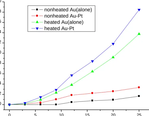
Figure 3.2 Effect of heating and addition of Pt ions on NP formation vs. Au3+ reduction. It „s seen that both heating and Pt ions addition increases NP formation without affecting reduction rate. ... 36
Figure 3.3 Structure of benzophenone ... 37
Figure 3.4 UV-Vis spectra of PMMA/Au films with and without benzophenone taken in appropriate time intervals ... 37
Figure 3.5 UV-Vis spectra of PVA/Ag films with and without benzophenone taken in appropriate time intervals ... 38
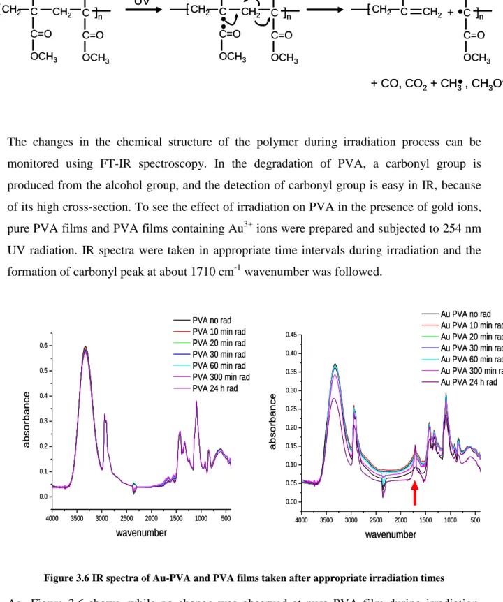
Figure 3.6 IR spectra of Au-PVA and PVA films taken after appropriate irradiation times ... 39
Figure 3.7 Reduction of Au3+ in PMMA by different wavelengths of UV-Vis radiation ... 40
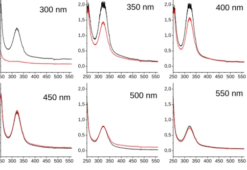
Figure 3.8 Reduction of Au3+ in PVA by different wavelengths of UV-Vis radiation ... 41
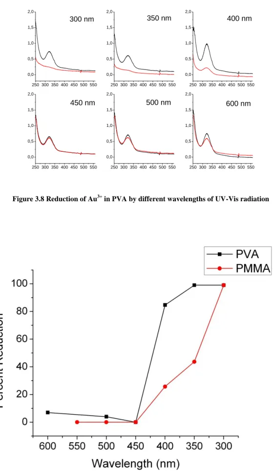
Figure 3.9 Graph summarizing the reducing effects of different wavelengths of light on PVA and PMMA. ... 41
Figure 3.11 Raman spectra recorded from different regions of the photo-patterned film on a silicon wafer substrate ... 44 Figure 3.12 Secondary electron (left) and backscattered electron (right) images of a
photopatterned Au-PMMA film ... 45 Figure 3.13 Light microscope image of photopattern produced on Au-PMMA film by 200 μm x 200 μm mesh, the film was irradiated for another 24 hours after the mask was removed. ... 46 Figure 3.14 SEM image of the photopatterned Au-PMMA film after second UV treatment .. 46 Figure 3.15 Illustration of ion migration during irradiation and the ion depleted region at the border, after mask is removed and after second UV treatment. ... 47 Figure 3.16 Fluorescence microscope image of a photo-patterned Au/R6G/PMMA film. ... 49 Figure 3.17 Fluorescence images of photo-patterned (a) Au-PMMA and (b) PMMA films with R6G taken by fluorescence microscope. ... 50 Figure 3.18 Fluorescence microscope images of PMMA with gold and R6G, the middle of which contains that of only R6G film overlapped. ... 51 Figure 3.19 Overlapped images of SEM and fluorescence microscope of the same sample ... 52 Figure 3.20 Fluorescence images of PMMA film with Au and R6G irradiated for 30 minutes, 1 hour and 24 hours. Inlet: XPS line scans of the Au4f peak intensity ... 53 Figure 3.21 Photo-patterned PVA film containing Au nanoparticles and R6G, left hand-side shows SEM image right hand-side shows fluorescence image. ... 56 Figure 3.22 The scheme of samples used for XPS measurement ... 58 Figure 3.23 Charging behaviour of C lines of PMMA films a) without gold nanoparticles, b) with gold nanoparticles and c) with a large amount of gold nanoparticles ... 59 Figure 3.24 Measurement of dielectric behaviour of Graphite, PMMA and Au NP/PMMA films with SQW voltages at different frequencies. ... 61 Figure 3.25 Off-set shift observed in the C lines of PMMA with and without gold
nanoparticles compared to line positions of Graphite as a reference ... 62 Figure 3.26 Snapshot spectra of PMMA/Au NPs film (left) and PMMA film (right) taken as a function of 0.01 Hz +/-10 V SQW voltage and the effect of flood gun. ... 63
Figure 3.27 IV measurement performed on PMMA film containing Au3+ ions and Au
nanoparticles ... 64 Figure 3.28 XPS spectra of carbon and oxygen 1s peaks of PMMA at Ground, -0.25 V and +0.25 V. ... 67 Figure 3.29 Fitted peak positions for dynamic measurement of -/+5 V at 0.002 Hz. (a)
Comparison of binding energy change of carbonyl carbon and backbone carbon. (b) Comparison of binding energy change of methoxy carbon and backbone carbon. (c)
Comparison of binding ... 68 Figure 3.30 Scheme representing the non-uniform distribution of charges on the PMMA surface. ... 70 Figure 3.31 Fitted dynamic XPS measurements performed on a PMMA film with and without flood gun. ... 71 Figure 3.32 Fitted dynamic XPS measurements performed on PMMA and Au/PMMA films without flood gun, with flood gun without Ar and with flood gun with Ar. ... 72
List of Tables
Table 3.1 Resistance and capacitance values calculated for Au NP/PMMA and PMMA films with SQW measurements ... 61 Table 3.2 Reference binding energies of C1s and O1s peaks for PMMA and the binding energy differences between the reference O1s and C1s values. ... 69
1 Introduction
Nanotechnology has been one of the most popular fields of science for the last 20 years and the attention towards this area continues to increase. Nanotechnology includes a wide range of applications in the interest of many different fields. For that reason, interdisciplinary approaches are generally essential for the creation of novel methods or materials within the scope of nanotechnology. “Nano” term in nanotechnology, in general, refers to materials with features in the 1 nm - 100 nm size range. In this size range materials behave differently from their bulk and atomic forms, hence materials which were previously unknown to us have been synthesized utilizing these properties. In addition to producing new materials, nanotechnology is also important to build smaller components for many applications like new generation electronics, computers etc.. In this respect, there is an ever-increasing demand for smaller components for technology with increased capacity to create more compact devices than before. Especially for the computers, the transistor technology we have now is not sufficient to build machines with higher capacity. New ways to fit more transistors or other circuit elements to smaller chips are required. To achieve this mission, scientists now use nanotechnology to create smaller and more powerful transistors, capacitors and other circuit components for such systems. Of course this example is only a very small fraction of the studies conducted in the field of nanotechnology. Such approaches to build smaller and more efficient materials are employed in many different fields like biotechnology, catalysis chemistry, environmental chemistry, sensor design, energy related research etc.
One of the most studied materials in nanotechnology is probably metal nanoparticles, sometimes referred as Quantum Dots (QD) as well. Nanoparticles are basically particles made of any material that are again within the size range of 1-100 nm. The reason of the demand for nanoparticles in various applications is their fascinating size-related properties. 1-3 Each metal nanoparticle behaves different and has specific properties depending on its size, shape and composition. The electronic properties of metals differ drastically, as one compares bulk metal to metal nanoparticles and molecular forms of the metals, due to change in density of electronic states as shown in Figure 1.1.4, 5. Nanoparticles neither have bandgaps as wide as molecules nor as small as bulk metals. The bandgap structure of most nanoparticles can be described as discrete energy levels with a small energy gap. This change in the bandgap structure grants many different properties to the nanoparticles. In addition, the increased
surface/volume ratio imparts some nanoparticles more reactivity than their bulk counterparts and enables them to catalyze reactions more efficiently and/or some nanoparticles gain superior electrical properties making them excellent candidates for the next generation electronic devices. Of course how their properties change is strongly related to the material they are made of. Nanoparticles can be synthesized from noble metals atoms like gold, platinum or silver or transition metals like manganese, iron etc. or even the oxides of the transition metals. In addition to that, nanoparticles consisting of two or more different metals can also be synthesized. Core-shell nanoparticles and alloy nanoparticles are examples for this kind of nanoparticles. Creating such bimetallic (or multimetallic) nanoparticles enables us to achieve properties that cannot be achieved with monometallic nanoparticles. Whatever they are made of, the band structure imparted in nanoparticles is particularly important and enables many applications in electronics3, 6, optics7, 8, catalysis9, 10 and biotechnology11, 12.
Figure 1.1 Evolution of electronic states of a metal from molecule to bulk
As mentioned, nanoparticles of noble metals like gold or silver can be synthesized and they have exciting chemical, optical and physical properties unlike their bulk metals. For example, although the bulk form of gold is an inert material, the nanoparticle form of gold is highly reactive and can catalyze many different reactions. 13-16 Also they have interesting optical properties. A strong absorption band in visible range is observed for most of these noble metals, which is called Surface Plasmon Resonance (SPR) band. SPR band is usually a very strong absorption band which makes the nanoparticles having this band, especially in the visible range, very valuable for optical applications. In the upcoming chapters, the extraordinary properties of gold nanoparticles and the applications related to these properties will be discussed in more detail for a better understanding of the motivation for this work.
.
Molecule
Nanoparticle
Metal
Band gap
Molecule
Nanoparticle
Metal
1.1 Applications of Gold Nanoparticles
Although gold nanoparticles have become popular for the last decade but they are not newly discovered. They have been used by many cultures from Egypt to China as a colorant for glass or ceramics throughout the history. We can still admire stained glass windows in churches colored with colloidal gold from centuries ago. Considering the elapsed time we‟ve been using gold nanoparticles, the detailed characterization to classify them as nanoparticles is very recent. After realization of the special electronic structure of gold nanoparticles and introduction of synthesis methods with excellent control on the particle size and shape, the research considering the possible applications of gold nanoparticles has increased tremendously for the last 50 years. Nowadays gold nanoparticles are even being used in some commercial applications created with certain nanotechnology approaches. There are also numerous applications of gold nanoparticles in different fields. Brief insights to some of these fields will be mentioned in the following sections to demonstrate the importance of gold nanoparticles in science and technology.
1.1.1 Gold Nanoparticles in Electronics
In the electronics, the most demanding objective is to build smaller devices with higher performance and with less energy consumption. The current semiconductor technology cannot fulfill these requirements any further since it has reached its physical limit. In place of the current systems, more capable new materials should be developed. An important candidate for such technologies is single electron device concept, which uses quantum dots as its components. The single-electron devices are expected to employ “switchable” quantum dots and quantum channels with correlated electrons that can offer order of magnitude smaller components for the new generation electronics. This can result in new generation of computers, supersensitive electrometers, near infrared receivers and very simple miniature lasers. Gold nanoparticles can be employed to produce such devices as shown in a study by Sato et al. in which a single-electron transistor has been constructed using alkanedithiol-stabilized gold nanoparticles as tunnel junctions.17
When metallic nanoparticles with a diameter in the range of a few nanometers are arranged with an interparticle distance of about 1nm, they build tunnel junctions with low electrical capacitances. 18 With this process controlled charge transport between the particles can be achieved by single-electron tunneling (SET) events at room temperature. SET devices can range from a single conductive nanoparticle between two microelectrodes to 2D-3D
arrays of nanoparticles with SET property in contact with a STM tip. For example, scanning tunneling spectroscopy has been used to observe SET effects on nanoparticle monolayers of Au55 nanoparticles in contact with a tip and “Coulomb staircase” behavior (single electron
transfer steps in current-potential curve) was observed even at room temperature and the capacitance of the nanoparticles was calculated as 3.9 x 10⁻¹⁹ F. 19 Combining many SET elements to develop computing devices is still challenging. Although construction of single nanotransistors is not a hard task, combining 1012 transistors to form a transistor network is yet a dream. But judging from the current studies, gold nanoparticles are excellent candidates for the components of such devices.
1.1.2 Gold Nanoparticles in Catalysis
Normally gold is known as a chemically inert element and indeed it is one of the most stable elements. But gold nanoparticles are surprisingly very active catalysts for many different reactions. For example, Haruta et al. reported that gold nanoparticles dispersed on Co3O4, Fe2O3 or TiO2 substrates are highly active catalysts for CO and H2 oxidation, NO
reduction, water-gas shift reaction, CO2 hydrogenation and catalytic combustion of methanol. 13-16
This surprising catalytic activity again is a result of the intermediate electronic structure of gold nanoparticles between bulk metal and atomic state. Catalytic performance can be sensitive to particle size since the surface structure and electronic properties can change greatly with the size of the nanoparticles. One of the most important studies about gold nanoparticle catalysts was by Valden et al. 20. They produced a highly active model gold catalyst where gold nanoparticles are spread uniformly on a Ti2O3 surface that showed ~50
fold improvement in the performance of realistic, high surface area catalysts.
Besides improved electronic structure suitable for catalysis, gold nanoparticles are also preferred as catalysts for their large surface/volume ratio. For catalysis the area of the catalyst interacting with the substrate is of great importance. For the same amount of catalysts the ones with larger surface/volume ratio have greater activity than the others if all other conditions are equal. For this reason generally catalyst species are attached to mesoporous or microporous structures for heterogeneous catalysis to achieve the largest possible area for interactions with the substrate. In this aspect, gold nanoparticles serve as a practical solution for this problem with their easy synthesis and naturally large surface/volume ratio. 1
For instance a final note on catalysis with gold nanoparticles is, as can be realized from the list of the important reactions that are catalyzed by gold nanoparticles, most of the
reactions are related to degradation of harmful gases that cause air pollution and global warming. For this reason gold nanoparticle based catalyst research is a very hot topic and better catalysts for the exhaust of the cars or other pollution sources are anticipated in the near future.
1.1.3 Gold Nanoparticles in Biotechnology
Gold nanoparticles are also widely used in biology and biotechnology for various applications, mostly on the basis of attaching different groups on nanoparticles and functionalizing them as sensors or for targeted drug delivery. Currently, DNA-gold nanoparticle assemblies for biological sensors, gold nanoparticle enhanced immuno-sensing, gold nanoparticle sugar sensors and other gold nanoparticle bioconjugates like peptides, lipids, enzymes, drugs and viruses are some of the areas of interests. Conjugates of gold nanoparticles with oligonucleotides are of great interest because of the potential use of the programmability of DNA base pairing to organize nanoparticles in space and the multiple ways of providing a signature for the detection of precise DNA sequences. With these properties such conjugate systems have many applications in the fields of biosensors, disease diagnosis and gene expression. 21 22 23 For example, in a study of Mirkin‟s group DNA and RNA oligonucleotides attached to gold nanoparticles was monitored using surface-enhanced Raman spectroscopy (SERS) and with the shifts of the corresponding Raman signals matching with the target oligonucleotides was detected. 24 Like this example, by changing the attached groups on gold nanoparticles many of the biological molecules could be detected since biological systems are generally based on pair matching mechanisms. Using this basis, it is possible to design biosensor chips, consisting of gold nanoparticles with different recognition groups as an array on the chip and a single drop of specimen can be detected for many different threads at the same time.
1.1.4 Gold Nanoparticles in Characterization
Gold nanoparticles are also used for the improvement of instrumentation techniques and detection methods. The mostly known example in this area is SERS effect of gold nanoparticles. 25 Generally Raman signals of most molecules are hard to detect since the signals are very weak and the concentration must be very high to conduct a reliable measurement. But for cases like molecular biology generally the amount of the molecule to be detected may be very small and some kind of signal enhancement is needed at such cases.
Surface plasmon resonance of gold nanoparticles enhances Raman signals and enables non-detectable amounts of materials to be detected.
Besides, gold nanoparticles can also be used for analytical detection of desired elements or molecules, changing the attached groups. An example of such studies is given by Kim et al. for detection of small concentrations (“spectroscopically silent”) of aqueous heavy metal ions, including toxic metals like lead, cadmium, mercury, was accomplished using simple calorimetry. 26 In this study, functionalized gold nanoparticles were aggregated in solution in the presence of divalent metal ions by an ion-templated chelation process and this caused an easily measurable change in the absorption spectrum of the particles.
1.2 Applications of Nanoparticle-Polymer Composites
Polymer composites have been produced and used for decades for various applications. Probably the most famous and widely used polymer composite is Bakelite, which is a clay reinforced resin that was developed in the early 20th century. Nevertheless the true importance of polymer composites was not fully realized until the end of 20th century. With the growing attention towards nanomaterials such as nanoparticles, carbon nanotubes and nanowires, the investigations towards possible applications of these materials in polymer composites has also became popular. Addition of nanoparticles or other nanomaterials to the polymer matrix enables the modification of polymer properties or sometimes implies addition of new properties to the polymers. These new materials with superior properties have many applications in different areas like optics, microelectronics, piezoelectrics, batteries, organic solar cells and biomedical sciences etc. and the application areas still continue to increase. Some of the most popular applications will be reviewed briefly in this section.
There are several ways to produce polymer-nanoparticle composites depending on the desired properties and the area of use. Nanoparticles can either be integrated to the polymer matrix to produce homogeneous composite films or can be capped with polymers to produce nanoparticle-core/polymer-shell composite nanoparticles. To produce homogeneous composite films of polymer-nanoparticle composites nanoparticles can either be synthesized beforehand and integrated to the polymer or can be synthesized within the polymer. For both cases homogeneous distribution of the pre-synthesized nanoparticles is important. In the former synthesis method, ligands that are used to stabilize nanoparticles against agglomeration, can be immiscible with polymer and prevent homogeneous distribution in some cases. The ligand choice should be carefully made for the synthesis of nanoparticles for that reason. However in the latter case, which is the synthesis of the nanoparticles directly within the polymers, the homogeneous distribution of nanoparticles in polymer is granted for most cases. Comparing the distribution of metal pre-cursors to nanoparticles, the distribution of metal pre-cursors can be more easily achieved because of their small size and high miscibility with the polymer.
Another important criterion to be watched for the nanoparticle-polymer composites is maintaining the interaction and full integration of nanoparticles in the polymer matrix. In this case ligands around the nanoparticles can again be a problem since even if the ligand is
miscible with polymer and enables homogeneous distribution, it still forms a barrier between nanoparticle and polymer. Especially in applications for electronics, full integration of nanoparticles with the polymer is needed for improved electron transfer between nanoparticles and polymer. For this reason ligand hinderance should be kept at a minimum. The synthesis of nanoparticles inside polymer matrices is again advantageous for such cases since the nanoparticles synthesized with this method in the polymer don‟t need ligands for the stabilization. Polymer maintains the particle size of nanoparticles and prevents them against agglomeration by its limited pore size and low diffusion rate within. For that reason better interaction of polymer with nanoparticle can be maintained using this synthesis technique.
One of the most important effects of nanoparticles on polymer materials is changing their optical properties. For example, the addition of nanoparticles can change the refractive index of the polymers, as shown by many different studies27-32. TiO2 is one of the most widely
used materials to modify the refractive index of the polymers, but there are also studies employing ZrO2, Al2O2, ZnO and PbS for this purpose. The modification of refractive index
of polymers is especially important for applications like microoptics and optical data transmission. Photoluminescence of nanocomposites is another interesting property of nanoparticle-polymer composites and it has a high potential for applications. For example epoxy nanocomposites containing ZnO nanoparticles can be used as solid state lightning33 and ZnO-polymer core-shell nanoparticles can be used for in vitro cell imaging34.
Combination of Fe2O3, Fe3O4 or ferrite nanoparticles with polymers creates the
opportunity to produce polymeric materials with magnetic properties. Polymer nanocomposites with desired magnetic properties free of hysteresis at room temperature and in some cases transparent can be produced this way.35, 36 For polymers with magnetic properties there are many potential applications in different fields such as in industry; as microwave absorbing material37, as contrast agent for magnetic resonance imaging38, 39, in cancer treatment by local hyperthermia40, 41, as drug carriers42, 43 or as biocompatible ferromagnetic fluid44, 45.
Polymer composites with interesting dielectric properties can be synthesized with the addition of conductive metal nanoparticles to polymers. The most aspiring advantage of using polymer composites as parts of integrated circuits is the opportunity of “printing” the polymers on the boards to create these circuits. Such an opportunity would bring down the production costs tremendously compared to the current technology. Also polymers can be synthesized with low cost methods and there is practically unlimited amount of resources
compared to the limited resources of silicon, which is used as the base material of the current electronic devices. Additionally light and flexible devices can be produced using polymer composites as the main material which is an advantage regarding the preferences of the consumers towards such products. Studies continue to grow aiming to produce suitable nanocomposites as components for electronic applications. 3, 46 For example there are many attempts to design materials with high permittivity to be used as capacitors. BaTiO3
composites with polymers are promising candidates for such applications because of the high permittivity of BaTiO3. 47, 48 In another study the capacitive and resistive characteristics of
ionic polymer metal composites are discussed in length. 49 Although there are encouraging examples of polymer composites demonstrating excellent capacitance or conductance abilities for the design of circuit components, the integration of those into circuits and devices still has a long way to go and studies will continue to overcome many hardships in this way.
Another important potential application field for the polymer-nanoparticle composites is employing them as electrodes in lithium-ion batteries. Nanocomposites based on inorganic nanoparticles and carbon are very advantageous as anode materials in lithium-ion-batteries and are expected to increase the performance of the batteries significantly since reducing dimensions using nanomaterials increases the diffusion rate of lithium insertion and removal due to short diffusion lengths. 50 Also the electron transfer between nanoparticles is enhanced and the high surface/volume ratio enables high contact area with the electrolytes. Nanocomposites containing SnO2 seems very promising as anode materials since they have
higher specific capacities than the standard carbon anodes. The most important point to improve about nanocomposite anodes is the cyclability of the anode. The current cyclability of the nanocomposites are quite low comparing to the current systems and studies to improve this problem continue. Combining nanoparticles with carbon based materials gives promising results for increasing the number of cycles the anode can go through. Zhang et al. demonstrated a high number of cycles (100 cycles with 34% decay) for metallic Sn nanoparticles encapsulated in an elastic carbon sphere. 51Carbon encapsulation of SnO2 also
1.3 Synthesis of Nanoparticles
Synthesis methods for nanoparticles are typically grouped into two categories: (i) top- down and (ii) bottom-up approaches. The top-down approach involves division of a bulky solid into smaller portions, using milling, chemical methods and volatilization of a solid followed by condensation of the volatilized components. The bottom-up approach uses condensation of atoms or molecular species from the gas phase or the solution. Both methods have advantages and disadvantages in different aspects. The top-down approach employing lithography and etching techniques can advantageously be used to generate required nanostructures in a spatially controlled manner. This property is important for integration and interconnection of nanoparticles into circuit elements and/or to design other specific applications. On the other hand, the bottom-up approach is very powerful in creating monodisperse nanoparticles with atomic precision and this precise synthesis is important for applications in need of well-defined nanoparticles. Also the machinery and the costs of both approaches differ considerably. For the top-down techniques generally expensive machinery and careful maintenance are needed. While for the bottom-up techniques, reactions generally take place in a test tube and the cost of reagents are a lot cheaper compared to the costs of machinery used in the top-down approach. There are strong and weak sides of both approaches and one would select the most suitable method for their own application.
1.3.1 Synthesis of Gold Nanoparticles in the Solution Phase
As mentioned before, nanoparticles can be produced with many different techniques, gold nanoparticles are no exception to that. Nevertheless solution phase synthesis is the most commonly used synthesis approach for gold nanoparticles, because of its well defined nature and the accuracy of the synthesized nanoparticles.1, 53 The solution phase synthesis generally consists of two steps; reduction of gold salt ions in the solution with a mild reducing agent and capping the nanoparticles with an organic molecule to prevent the further agglomeration of the particles. The reducing agent reduces Au3+ ions to Au0 atoms and Au0 atoms coalesce to form nanoparticles since they are thermodynamically more stable. To prevent further aggregation of the formed nanoparticles, organic capping agents are used to result in stable and dispersed nanoparticles.
Among the commonly used synthesis methods of gold nanoparticles the most popular one is Turkevitch method, introduced by Turkevitch in 1951.54 The Turkevitch method
employs citrate reduction of HAuCl4 in water. Gold nanoparticles of about 10-30 nm can be
synthesized with this method. Also a method for the synthesis of nanoparticles with pre-chosen size was introduced by Frens in 1973. 55 It was shown that the derivation of the ratio between the reducing/stabilizing agents can lead to nanoparticles size between 16 nm – 147 nm size range. Turkevitch synthesis is generally used to produce nanoparticles with a loose shell of ligands (citrate ions) around the gold nanoparticle core.
Another method used widely for gold nanoparticle synthesis is the Brust-Schiffrin method. 56, 57 This method was proposed in 1994 and had quite an impact on the field since it enabled the facile synthesis of thermally stable and air-stable gold nanoparticles with reduced dispersity and controlled size for the first time. Nanoparticles synthesized by this method can be repeatedly isolated and redissolved in common organic solvents without aggregation and decomposition so they can be easily handled like stable organic molecules. This synthesis method uses thiol ligands that strongly bind gold, because of the soft character of both gold and sulfur. AuCl4- is transferred to toluene using tetraoctylammonium bromide as the phase
transfer agent and reduced by NaBH4 in the presence of dodecanethiol. The color of organic
phase changes from orange to deep brown within a few seconds upon the addition of NaBH4.
Gold nanoparticles synthesized with this method are in the size range of 1 nm – 3 nm, the size of the nanoparticles can be controlled adjusting the gold/thiol ratio and also the temperature of the reaction medium. Fast reductant addition and cooled solutions produce smaller and more monodispersed nanoparticles with this method.
Other than the synthesis methods mentioned above there are many other methods to produce gold nanoparticles with pre-chosen size and morphology. In these methods the size and shape of the nanoparticles are generally controlled by changing the medium temperature, the concentration of gold salt, the concentration of the reducing agent, adding reactants slower or faster or by variation of stirring conditions.
Thus, using solution phase synthesis methods, particle size, composition and life-time of nanoparticles may be controlled very accurately. However integration of the synthesized nanoparticles into solid materials like polymers or films is a big problem for this synthesis method if one wants to produce nanoparticle-polymer composites. Especially the spatial control on the distribution of nanoparticles throughout the polymer matrix is very hard using this synthesis method.
1.3.2 Synthesis of Nanoparticles in Polymer Matrix
Polymer-nanoparticle composites are important candidates for new age technological devices as mentioned in the previous sections and ongoing research by many different groups is performed for production and characterization of these systems. Polymers can be used as platforms to support gold nanoparticles as substrates. For example, in many biological applications polymers are used as carrying media for nanoparticles to their targets, or in catalysis polymers can be used as supports for nanoparticle catalysts. As much as polymers are good candidates for supporting nanoparticles, nanoparticle-polymer composites can also be functionalized to produce new materials using both properties of gold nanoparticles and polymers. Flexible, low weight, advanced electronic devices can be designed using such materials in the production. But as mentioned before the primary problem that we must overcome to produce such systems is the integration of nanoparticles in to the polymers homogeneously and for some applications with a spatially controlled manner.
Nanoparticles may be synthesized before the integration to polymer or within the polymer to produce composite systems. For example, Vitale et al.58 synthesized Au nanoparticles and dispersed these dodecanethiol functionalized Au nanoparticles, in poly[platinum-bis(tributhylphosphine) diethynylbiphenyl] afterwards, whereas Horiuchi et al. demonstrated that Pd nanoparticles may be produced in polymethylmethacrylate films, through adsorption of Pd(acac)2 vapor to irradiated polymer films.59 With the method
proposed by Horiuchi et al. patterned polymer films of diblock-co-polymers or polymer blends can be produced using the varying adsorption tendencies of Pd(acac)2 vapor to
different polymers. However, this process needs high temperature conditions (180oC) for the evaporation of Pd metal into the polymer matrix thus is not appropriate for systems working at room temperature.
At room temperature, an efficient approach, used for the production of nanoparticles within the polymer matrix is employment of irradiation. Energetic light is a widely used element to produce electrons within in the synthesis medium for reduction of metal salts and it is both used in the solution phase synthesis as well as, in the solid state synthesis. Gachard et al. has reported a synthesis method, which employs γ-rays to induce reduction in an aqueous solution of 2-propanol and polyvinyl alcohol with gold salt.60 In another study, we reported that x-rays can also be used to reduce gold ions into gold atoms followed by formation of gold nanoparticles61. Not only highly energetic light like γ-rays and x-rays are employed for reduction, but also less energetic UV irradiation can also be used for this
purpose. Korchev et al. proposed that silver nanoparticles can be produced in sulfonated poly(ether−ether)ketone−poly(vinyl alcohol) films by direct irradiation with 350 nm UV light62. Alexandrov et al. used UV light to initiate the gold nanoparticle growth in PMMA films and finalized the synthesis by annealing the samples at different temperatures from 20oC up to 80oC63.
In our work, we used light of various wavelengths to produce electrons within the polymer matrix to reduce gold ions into gold atoms. The produced gold atoms then, nucleate and grow into gold nanoparticles inside the polymer matrix(Figure 1.2). During the irradiation of the polymer, cross-linking of the polymer also takes place and this process may limit the growth of the nanoparticles after a critical particle size. This in-situ reduction method
Figure 1.2 Schematic representation UV radiation induced, reduction of Au3+ ions to Au0 atoms and nucleation and growth of Au nanoparticles in polymer matrix
has many advantages and enables different applications. With this method we can overcome a very important obstacle in the nanoparticles/polymer composite studies, which is the integration of nanoparticles to the polymer films after their synthesis. As much as it benefits from the degradation of the polymer, this method doesn‟t destroy the polymer completely, and only a very small percentage of the polymer is degraded. Also with this method reduction process and nucleation and growth processes of gold can be entangled and followed step by step with UV-Vis spectrometer since the rates of these processes in polymer are much slower than in solution, in which gold ions are reduced instantly and nanoparticle formation is completed in the following minutes. Photo-patterning and direct writing are possible applications and another advantage of this production method. Using a light impermeable mask, patterns of all sorts and of a large range of sizes can be imprinted on the polymer.
Au0 Au0 Au0 Au0 Au0 Au NPs Au3+ Au3+ Au3+ Au3+ Au3+ Au 3+ Au3+ Au3+ Au0 Au0 Au0 Au0 Au0 Au 0 Au0 Au0 UV UV UV
Reduction Nucleation Growth
e -e -e -e -Au0 Au0 Au0 Au0 Au0 Au NPs Au3+ Au3+ Au3+ Au3+ Au3+ Au 3+ Au3+ Au3+ Au0 Au0 Au0 Au0 Au0 Au 0 Au0 Au0 UV UV UV
Reduction Nucleation Growth
e
-e
-e
-1.4 Advantages of Poly(methyl methacrylate) as a Synthesis Medium
PMMA is a well known, utilized and extensively studied polymer, which is an important dielectric element in electronics. One of the advantages of using PMMA as a substrate is the ease of processibility and preparation of PMMA films. PMMA can be dissolved in acetone relatively easier compared to the dissolution of other polymers in their particular solvents. Acetone was selected as the solvent since it can both dissolve PMMA and HAuCl4 and is not as hazardous as other organic solvents. Film preparation with acetone is
also fast and easy since acetone can evaporate at room temperature very quickly compared to many other solvents.
Besides the ease of preparation, PMMA is also appropriate for its stability. PMMA matrix is more rigid compared to many other polymers, hence nanoparticles can be confined to specific sites after their preparation within the matrix. For example, PVA was also used in our studies in earlier stages and for specific purposes and gold nanoparticles can also be prepared in PVA matrices, but our experiences showed us that PVA films containing gold nanoparticles were not as stable as PMMA films. There were also reports concerning this fact in the literature. 64 After their preparation PMMA films conserve their spectroscopic properties for a long time (3 years of stability was observed until now). For PVA films change in the absorption of surface plasmon resonance band was observed after 1 year and distortion on the photo-patterns printed on PVA was also observed. On the other hand, photo-patterns printed at PMMA films were stable.
1.5 Photo-Patterning of Polymer Composites
Patterning of polymer composites is a technologically important process for many different applications. In polymer-nanoparticle composite preparation, besides being able to achieve homogeneous distribution of nanoparticles inside polymer films for successful composites, pattern creation on or in polymer films using nanoparticles is another important issue, especially for optical and electronic applications. There are many different techniques employed to create patterned polymer films. One of the most used techniques for achieving patterns, consisting of regions with and without nanoparticles, is to use the immiscibility of various polymer blends to selectively adsorb nanoparticles in one of the immiscible polymers. In such a study Horiuchi et al. demonstrated the selective reduction Pd(acac)2 vapors by
poly(styrene)(PS) matrix in PMMA-PS blends. 59 They subjected PS-PMMA blends to Pd(acac)2 vapor in N2 atmosphere, the blend adsorbed Pd vapor and only PS matrix
selectively reduced Pd ions to Pd nanoparticles because of the PS‟s high reduction power towards Pd ion. PMMA matrix on the other hand didn‟t produce any Pd nanoparticles since the reduction power of PMMA is rather low. This study showed with selective production of Pd nanoparticles by different polymers in a blend, one can produce patterned films according to the blend‟s structure. Nevertheless the control on the pattern morphology is very hard to achieve with such a technique. In another study, Horiuchi et al. found a way to increase PMMA reducing power externally to modify the printed patterns. 65 In which they subjected PMMA films to UV irradiation for an increased reduction power of PMMA towards adsorbed Pd ions and with this method they produced patterns consisting of UV irradiated Pd nanoparticles containing regions and non-irradiated Pd ion containing regions.
Another technique that can be used to achieve such patterns on polymer films is to start with a dispersed metal precursor and selectively reducing required regions for the pattern to produce nanoparticles within. 66 This technique is the one we used to produce patterns consisting of regions with and without gold nanoparticles within the PMMA matrix. With this technique using a photomask impermeable to light, any pattern can be printed on the polymer films consisting of regions with and without nanoparticles. The stability of the printed patterns is an important issue in this technique and the production of stable patterned films was achieved and this issue will be discussed in the upcoming chapters.
1.6 Ultraviolet-Visible Spectroscopy
Ultraviolet-Visible (UV-Vis) spectroscopic technique measures the absorption spectra of samples in the ultraviolet and visible range of the electromagnetic spectrum by recording the amount of light adsorbed by the sample in different wavelengths. The absorption spectra in this range include electronic transitions which are generally the transition of an electron from a ground state to an excited state in the molecular orbitals. In addition, some vibrational transitions may also be observed when the spectrum is of a gas phase molecule. The electronic transitions observed in the UV-Vis spectroscopy generally appear as broad peaks because of the interactions of molecules with each other and the solvent molecules. For example the UV-Vis spectrum of a molecule dissolved in water, generally includes the effects of hydrogen bonding and molecular interactions in addition to its own electronic transitions. To get rid of this broadening is only possible if the spectrum is recorded in gas phase and/or in inert matrices, but this may not be possible for many samples.
UV-Vis spectroscopy is a widely used technique since it‟s very easy to use and relatively cheap compared to many other techniques and can give valuable information for different types of samples. The most fundamental formulation used in UV-Vis spectroscopy for the quantification of measured absorption values is the Beer-Lambert law:
In this formulation, A is the measured absorbance at a specific wavelength, is the molar absorptivity or extinction coefficient at a specific wavelength, b is the path-length through the sample and C is the concentration of the absorbing species. Thus, one can calculate the concentration of the absorbing species in a sample by simply measuring the absorption of the sample and using the molar absorptivity at a specific wavelength. Of course the only information UV-Vis provides about the sample is not its concentration. At least, the applications of UV-Vis spectroscopy in nanotechnology are more. Especially, in the nanoparticle characterization UV-Vis spectroscopy is widely used for the determination of many different properties. For example, for quantum dots, the UV-Vis spectroscopy can be used to calculate the average particle size and more importantly the band-gap of the nanoparticles. The particle size has an important role in the determination of the absorption spectrum in UV-Vis range, since, even though the material which makes up a nanoparticle, defines its intrinsic energy signature, the effect of nanoparticle's size significant at energies near the bandgap. The noble metal nanoparticles like gold or silver are also no exceptions.
They have distinct surface plasmon resonance bands in the visible region, which gives them their characteristic color. Surface plasmon resonance band will be discussed in length in the following section.
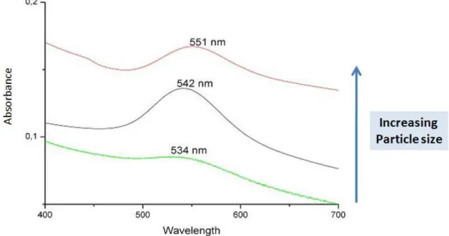
1.6.1 Surface Plasmon Resonance Band of Gold Nanoparticles
As mentioned above, nanoparticles of noble metals like silver and gold have very specific absorption peaks in the visible region called surface plasmon resonance (SPR) band, which make those nanoparticles important in optical applications. SPR band originates from the quantum size effect of the nanoparticles, since nanoparticles have neither atomic nor metallic electronic properties, because of their confined energy levels. Their electronic properties strongly depend on the particle size, interparticle distance, nature of the protecting shell and the shape of the nanoparticles. The quantum size effect is seen when the de Broglie wavelength of the valance electrons is of the same order as the size of the particle itself. When this happens, particles behave electronically as zero-dimensional quantum dots. Freely mobile electrons get trapped in such metal boxes and show a characteristic collective oscillation frequency of the plasma resonance, which is called surface plasmon resonance band.
For gold nanoparticles, the SPR band appears in between 500 nm – 600 nm depending on the particles size, and its position is strongly related to particle size as shown in Figure 1.3. Gold nanoparticles, smaller than 5 nm, are hard to distinguish and yield broad peaks as their SPR bands. But after 5 nm of particle size, SPR band becomes more easily noticeable. For smaller nanoparticles, the SPR band shifts to smaller wavelengths which is called blue shift, and for larger nanoparticles SPR band shifts to higher wavelengths which is called the red shift.
The UV-Vis spectroscopy of gold-nanoparticles and gold ions will be frequently used for characterization purposes throughout the rest of the thesis.
1.7 X-Ray Photoelectron Spectroscopy
X-ray Photoelectron Spectroscopy (XPS) is a non-destructive technique that gives both quantitative and qualitative information about surfaces. In XPS, x-rays of known energy are directed to the sample and photoelectrons are ejected from the sample as a result. Those photoelectrons are collected by a detector and their energies are measured. This process is expressed with the following Einstein‟s relation;
EB = hν - EK - Φ
EB is binding energy of the ejected electron, hν is the energy of the incident photon, EK is the
measured kinetic energy of the ejected electron and Φ is the work function which relates to the minimum energy required to eject an electron from the solid matrix to the vacuum level. A schematic representation of a XPS measurement is shown in Figure 1.4. Subtracting the measured kinetic energies of the photoelectrons from the energy of x-rays gives us the binding energies of the electrons. Since binding energies are specific to each atom for its specific energy level, and elements besides hydrogen can be detected and their relative amounts can be easily determined with this technique. Chemical specificity is a big advantage of XPS. Besides determination of the types of atoms on the surface, XPS can even give information about the oxidation states of those atoms. The chemical state of the atoms strongly influences the binding energy of the ejected electrons. The binding energy would be large for tightly bound electrons, hence for positively charged species a larger binding energy than the neutral state is measured.
Figure 1.4 Schematic representation of XPS measurement
e -x-rays Sample Detector e -e-filament e -e -x-rays x-rays Sample Detector e -e-filament e -e -e-filament
XPS is also a very surface sensitive technique. X-rays can penetrate through microns of depth into the sample, but ejected electrons without energy lost can only come from the top 10 nm or less (depending on the type of material the sample is made of) of the sample because the photoelectrons cannot travel through larger distances without loss of energy. To have information from depths deeper than 10 nm x-rays with high energies should be used and such measurements can be performed only at synchrotron facilities. Conventional XPS instruments usually work with x-rays at two different energies, Al Kα has 1486.6 eV and Mg Kα has 1253.6 eV x-ray energies.
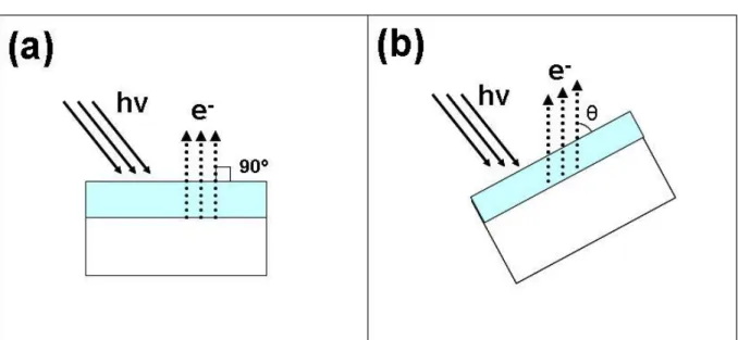
Using the small mean free path of the electrons, some additional information may be extracted using angle resolved XPS. Angle resolved XPS measurements are made at different take-off angles of electrons and at different angles the electron yield coming from a certain depth changes according to the angle. Figure 1.5 shows an angle resolved XPS measurement schematically. For instance, if we make the measurement at 90o (Figure 1.5(a)), this corresponds to the normal XPS measurement and a mean free path of d can be achieved. But if we decrease the angle to θ, we start to collect more electrons from the surface and the sampling depth equals to d.sinθ. As the mean free path decreases, our surface sensitivity increases and we can distinguish topmost layers on our sample.
1.7.1 Using Charging as a tool in XPS
In XPS measurements, a current is generated by the flow of photoelectrons and secondary electrons from the sample to the vacuum. Normally, the generated charge on the surface of the sample is neutralized by the electrons coming from the ground and no effect of this charging is seen through the measurements. But if the sample is non-conducting, the neutralization of the surface charging cannot be achieved and shifts at line positions are observed during the measurements, because of the charging. In the early years of XPS experiments, the charging of non-conducting samples had been considered as a nuisance and many successful techniques were developed to overcome this problem. For example, an electron filament can be added to the system to generate extra low energy electrons for the sample to ease the neutralization as shown in Figure 1.4.
Indeed charging phenomena causes shifts in the binding energies and inconsistent results can be produced. But it is also proved to be true that when used correctly, additional information about the samples can be harvested using charging as a tool. Applying external voltage bias to the sample during a XPS measurement causes shifts in the positions depending to the nature of the sample. For conducting samples positions shift as much as the applied bias, but for non-conducting samples the shift is observed to be nonlinear due to charging. This nonlinear behavior contains additional molecular and structural information. For example, it was shown by Ulgut et al.,67 that the thickness of SiO2 films on Si substrates can
be measured, with the application of positive and negative biases to the sample. Also in another paper the structure of a composite film was extracted again using charging as a tool for extracting additional information.68
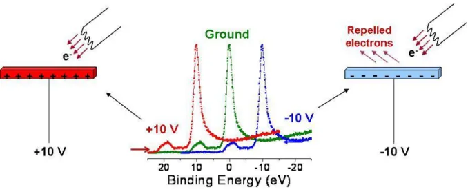
One way to use charging in XPS is applying a DC bias to sample at various voltages. For conducting samples if +10 V is applied to the sample an exact 10 eV shift towards higher binding energy is observed for its corresponding lines, this process is shown in Figure 1.6. If we have a non-conducting sample, according to its charging properties a smaller shift is observed in its line positions. This result points out the accumulated negative charge on the surface. When positive 10 V is applied to the non-conducting sample, the line position shifts +10 eV, but the positive potential on the surface attracts more low energy electrons from its surroundings than normal, thus the line positions start to shift to lower binding energies depending on the resistance of the sample. Overall, line shifts are smaller than the applied
voltage. For negative potentials an opposite situation takes place. During measurement electrons are repelled from the surface by the negative potential, thus the already shifted line positions start to shift to even larger apparent binding energies because of the positive charging generated at the surface. Again the overall observation is the shifting of the lines to lower binding energies less than a -10 eV difference in the case of applied -10 V. Such measurements give us information about the resistance of the sample since in this case the resistance of the sample prevents electrons to neutralize the charges created on the surface.
Figure 1.6 Shifting of the XPS peaks due to +/- 10 V DC bias in a conducting sample.
Another method to generate charging on the sample surface and using it as an additional information source is applying square wave pulses to the sample. During DC potential measurements, we can get information about to what extent the sample can charge in the given potential interval but we can‟t predict how fast the sample responses to the potential changes. Knowing the response time gives us useful information about another electrical property of the sample which is the capacitance. Response times can be observed using potentials altering with different time intervals, and this can be easily achieved using square wave (SQW) pulses. SQW pulses are alternating potentials at a given frequency and with a given potential value. Generally +/- 10 V pulse is applied to the sample with different frequencies and in between 100 Hz to 10-3 Hz and data is collected. Since we apply two different potentials during data acquisition, we observe two peaks of a given line one for -10 V and one for +10 V. If the sample is not charging the binding energy difference between
these two peaks can be observed as 20 eV. But in the case of charging the binding energy difference between these two peaks starts to decrease with the increase in charging.
Basically the working principle behind the SQW potential and the DC potential measurements is the same. But for SQW potential measurements, additionally we can have information about capacitance property of the sample as mentioned before. The reason for that is in the case of SQW we can switch between negative and positive potential with a given frequency, thus we can see how quick the sample responses to the change of the potential in the frequency range we apply. For example, at high frequencies like 100 Hz, the potential switches from -10 V to +10 V so quickly that our polymeric samples cannot follow them , as a result we see no charging changes and observe an exact 20 eV binding energy difference, even though the sample itself maybe is in a charged state. Samples cannot find enough time to build up charge on them at frequencies so high. But for example, at frequencies like 10-2 Hz the potential switches from negative to positive at every 100 seconds, so the sample has enough time to build up charge and we can see binding energy differences smaller than 20 eV at such frequencies for non-conducting polymeric samples. The charge build up is of course different for every sample since this property depends on the dielectric properties of the sample, for example using this difference we can obtain capacitance for these samples by taking measurements at different frequencies and following the trend of each sample. At very low frequencies like 10-4 or 10-5 Hz the binding energy difference reaches to a point where it doesn‟t decay anymore and this point gives us the same binding energy difference as the DC potential measurements give. So SQW measurements give us information both on resistance and on capacitance of the sample.
1.8 Contact Electrification of Insulating Materials
The XPS charge resolved experiments performed on insulating materials like polymers, provides us a chance to investigate the response of insulating materials to charge accumulation on the surface. Finding out how the materials behave when surface is charged and how and where the charges are stored on the surface may give us important clues about the mechanism of electrification of insulating materials. Contact electrification of insulator materials is well known to men for a very long time, and is successfully used in many industrial applications. However, the detailed molecular nature of this phenomenon is still unknown to us. There are several studies proposing different mechanisms for the causes of electrification. 69-73 Among those, two major ideas emerges as the source of electrification. Some claim that electron transfer is the reason for the electrification, while the others think ion transfer takes place during rubbing or contact of two insulators and this is the source of electrification. There are convincing evidences for both sides and the case is still controversial.
Figure 1.7 Schematic representation of contact electrification.
The main reason for this continuing debate is the difficulty of characterizing the nature of the charge on an insulating material. The present methods generally give an idea if there is any net charge on the surface but they cannot tell whether this charge originates from accumulation of electrons or ions. To overcome this problem Liu et al. proposed chemical characterization of the charge by subjecting it to redox reactions. 74, 75 They showed that the charge on a PTFE surface can reduce ions like Ag+, Cu2+, Pd2+ after contacting with PMMA, offering a solid evidence for the presence of electrons. Likewise the rubbed PMMA can change the pH of a solution by proton transfer, showing the presence of exchanged protons on