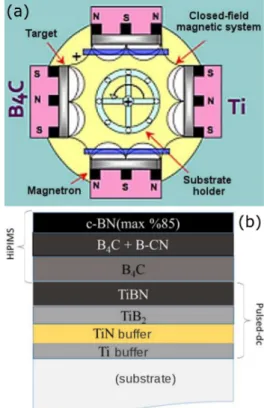
Characterization of Thin Film Boron Nitride Coatings and Observation of Graphite-Like Boron Nitride
Tam metin
Şekil

Benzer Belgeler
Nanowires of different sizes are initially cut from the bulk Si crystal in rodlike forms, and subsequently their atomic structures are relaxed before and also after the termination
It is explicitly shown with several examples that Godel-type metrics can be used in obtaining exact solutions to¨ various supergravity theories and in constructing spacetimes
methodology is combined to be suitable for interaction modeling between criteria using the concept of the bipolar Choquet integral [54], QUALIFLEX method is
Murat Bilir, "ben mesleğime aşığım, kendimi, zaman zaman bir masal dünyasında bulurum" derken, bu duy guyu benliğinde hissettiğini belli edecek kadar
Üryanizade Mosque overlooking the azure waters of the Bosphorus has an unusual carved wooden minaret (below).. köşesinde gevezelik eden ördeklerle, temkinli bir
If the induced current data obtained at the center of the body in Figure 33 was considered (since we use the magnetic field value at the center of the body in the quadrature
The exception to this general trend is found in the case of the fluorine substitution in the transition structures for inversion, where donation from the fluorine lp appears to
This result is in correlation with the caspase activity assay dem- onstrated in Figure 6 , suggesting that ALC67 treatment induced caspase-9 dependent apoptotic pathway resulting
