https://doi.org/10.1007/s00339-019-2402-6
On the elastic properties of INGAN/GAN LED structures
O. Akpınar1,2 · A. K. Bilgili1 · M. K. Öztürk1,2 · S. Özçelik1,2 · E. Özbay3
Received: 24 October 2018 / Accepted: 9 January 2019 / Published online: 18 January 2019 © Springer-Verlag GmbH Germany, part of Springer Nature 2019
Abstract
In this study, three InGaN/GaN light-emitting diode (LED) structures with five periods are investigated grown by metal organic chemical vapor deposition (MOCVD) technique. During growth of these three samples, active layer growth tem-peratures are adjusted as 650, 667 and 700 °C. These structures are grown on sapphire (Al2O3) wafer as InGaN/GaN multi-quantum wells (MQWs) between n-GaN and p-AlGaN + GaN contact layers. During growth, pressure and flux ratio of all sources are kept constant for all samples. Only temperature of InGaN active layer is changed. These structures are analyzed with high-resolution X-ray diffraction (HR-XRD) technique. Their surface morphologies are investigated with atomic force microscopy (AFM). Reciprocal space mapping (RSM) is made different from classical HR-XRD analyses. Using this method, mixed peaks belonging to InGaN, AlGaN and GaN layers are seen more clearly and their full width at half maximum (FWHM) values is determined with better accuracy. With FWHM gained from RSM and Williamson–Hall (W–H) method based on universal elastic coefficients of the material, particle size D (nm), uniform stress σ (GPa), strain ε and anisotropic energy density u (kJ m−3) parameters for the samples are calculated. The results are compared with literature. On the other hand, to have an idea about the accuracy of the results AFM images are examined. Parameters calculated showed differences but it is seen that the largest particle size is gained for GaN and the smallest is gained for AlGaN. For all parameters, it is seen that they increase for GaN layer and decrease for AlGaN layer with increasing temperature. For InGaN layer parameters, they showed both increasing and decreasing or decreasing and increasing behavior harmonically with an increase in temperature. Results showed that they are compatible with literature. Results gained from Scherrer and W–H are very near to each other.
1 Introduction
Aim of this study is to investigate the elastic properties of
InxGa1−xN/GaN MQW LED structures grown by MOCVD
with RSM and effects of these properties on the performance of such devices.
Optoelectronic devices with nitrides have great impor-tance in nanotechnology. Direct band gaps of InN, GaN and AlN are 0.7, 3.4 and 6.2 eV, respectively. These band gaps are in near infrared to ultraviolet region in electromagnetic spectrum [1]. With such properties, semiconductors with nitrides have importance in the development of devices
such as LEDs, laser diodes, microchips and photo detectors. These semiconductors with nitrides can operate in hard con-ditions as high pressure and temperature, and this is a good advantage [2]. InGaN LEDs have resistivity against high temperature, pressure and frequency. These structures are grown on silicon (Si) or sapphire (Al2O3) wafers tradition-ally. This growth causes cracks in the layers. The reason for these cracks is the lattice mismatch. This mismatch causes dislocations and the density of these dislocations is between 107 and 1011 cm−2 [3, 4]. In these types of structures, struc-tural defects can often be seen. To remove these defects, GaN buffer layer is grown between sapphire and InGaN/ GaN active quantum well layer. This operation eliminates the lattice mismatch that will be transferred to InGaN layer but it does not completely remove the lattice mismatch. Because of the mismatch between sapphire and GaN layer in the percentage of 15%, the transfer of threatening dislo-cations (TD) to InGaN active layer between the densities of 108–1012 cm−2 is inevitable [5, 6]. Although there are such negative properties, devices formed by semiconductors with nitrides have better performance [6].
* O. Akpınar
1 Department of Physics, Gazi University, 06500 Ankara,
Turkey
2 Photonics Research Center, Gazi University, 06500 Ankara,
Turkey
3 Nanotechnology Research Center, Bilkent University,
In this study, three InGaN MQW LED structures are investigated which are grown on (001) oriented sapphire wafer. All the parameters except growth temperature are kept constant during growth. To examine the structural proper-ties of the samples in more detail, diffraction pattern gained from HR-XRD is used. These patterns are transformed to RSM for symmetric and asymmetric planes. By the help of this method, defects in the structures are seen more clearly. In the calculations of this study cubic equation is used [7].
2 Experimental details
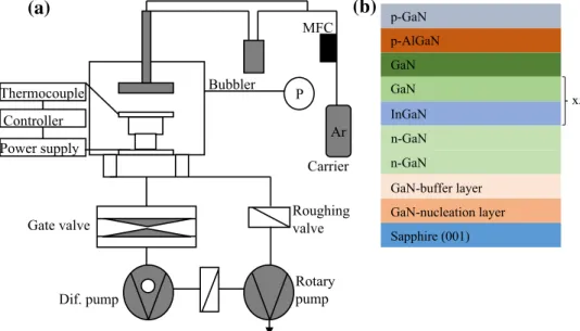
In this study, InGaN/GaN MQW LED samples are grown with AIXTRON RF200/4 RF-S MOCVD system. InGaN, GaN and AlGaN layers are grown on c-(001)-oriented sapphire substrate. Before the epitaxial growth operation, sapphire substrate is exposed to temperature of 1100 °C in nitrogen atmosphere for 10 min to remove the oxide layer on the surface of it [8, 9]. Trimethylgallium (TMGa), trimethy-laluminum (TMAl), trimethylindium (TMIn) and ammonia (NH3) compound chemical reactions are gained from Ga, Al, In and N sources, respectively. At 200 mbar pressure and at 500 °C temperature, GaN nucleation layer is grown on sapphire substrate [10]. Later at 1020 °C temperature, GaN buffer layer is grown. An n-type GaN contact layers are grown at 1030 °C with constant 23 sccm TMGa flux ratio. First layer of this contact layer is grown for 35 min and second layer is grown for 20 min. In 140 sccm TMGa and TMIn flux ratio, InGaN active layer of the samples A, B and C is grown at 650, 667, 700 °C, respectively, with a duration of first 90 s and later 390 s as five layers. Over these active layers, in 140 sccm TMGa flux ratio GaN cap layer is grown for 390 s at 730 °C. p-Contact AlGaN layer with
magnesium (Mg) deposition is grown for 65 s using 9 sccm TMGa, 15 sccm TMAl and 90 sccm Cp2Mg flux ratio. Dur-ing this operation, temperature is kept constant at 1085 °C and pressure is kept constant at 50 mbar. p-GaN layer is grown with 14 sccm TMGa and 100 sccm Cp2Mg flux ratio at 1010 °C and 200 mbar for 720 s. NH3 flux ratio is 1300 sccm for GaN, AlGaN layers and 5200 sccm for InGaN/GaN active layer (Fig. 1).
3 Results and discussion
In this study, particle size D (nm), uniform stress σ (GPa), strain ε, and anisotropic energy density u (kJ m−3) param-eters are calculated using RSM method. In classical calcu-lations, 2θ diffraction angle is kept constant in diffraction plane and rocking curve results gained by detecting the
θ angle are used often in literature [11–13]. Bruker axs D8 Discover brand HR-XRD device was used for XRD measurements.
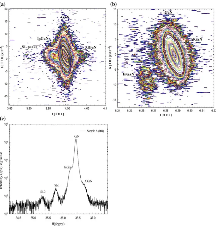
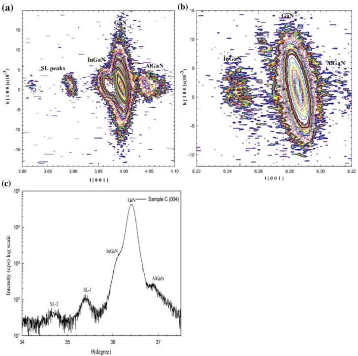
Patterns gained from RSM are clearer than classical HR-XRD peaks [2]. Mixed GaN, InGaN and AlGaN layer peaks can be distinguished from each other by the help of RSM. The comparison of classical HR-XRD pattern for samples A, B and C for (004) symmetric plane is given in Figs. 2, 3 and 4c and RSM of them is given in Figs. 2, 3 and 4a. If Fig. 2c is examined carefully, on the right of GaN peak AlGaN peak is not fully distorted but it can be seen in Fig. 2a clearly on the right of GaN peak. Again in the same figures, InGaN peak can be seen clearly on the right of GaN peak. By the help of RSM, satellite peaks (SL) can also be determined clearly. Generally, for RSM InGaN, GaN and AlGaN peaks are scanned for wide offset values and later these offsets are eliminated according to universal values of GaN. RSM
Fig. 1 a The schematic diagram
of the experimental installa-tion for the MOCVD system. b Schematic view of InGaN/GaN LED structure Ar Carrier P Bubbler MFC Power supply Gate valve Controller Thermocouple
Dif. pump Rotary pump Roughing
valve Sapphire (001)GaN-nucleation layer
GaN-buffer layer n-GaN n-GaN InGaN GaN GaN p-AlGaN p-GaN x5
(a)
(b)
pattern of sample A for symmetric (004) miller reflection plane is given in Fig. 2a. If this figure is examined carefully, on the right of the figure sapphire peak can be seen, and InGaN and AlGaN peaks can be seen mixed in GaN peak.
In Fig. 2b, RSM image of sample A for (106) asymmet-ric plane can be seen. If this image is examined, InGaN partly distorted from GaN and AlGaN not fully distorted can be seen. RSM image of sample B for symmetric (004)
miller reflection plane is given in Fig. 3a. If this figure is examined SL-1 and SL-2 satellite peaks can be seen together and InGaN, AlGaN peaks can be seen as more distorted from each other according to sample A. Here symmetric peaks are more dominant in (004) plane. Inter-ference of incident reflections caused from density differ-ence of GaN and InGaN layers forms these satellite peaks. These satellite peaks are related with crystal quality and
Fig. 2 a RSM of sample A in (004) symmetric plane. b RSM of sample A in (106) asymmetric plane. c XRD of sample A in (004) symmetric
surface roughness of inter-layers. They are used for deter-mining multi-quantum well thickness. Thickness calcula-tion can be made with the formula of T = 𝜆∕(2Δ𝜃 cos 𝜃) [14]. Here λ is the wavelength, Δθ is the SL distortion and
θ is the Bragg angle of the plane. RSM image of sample B
for (106) reflection plane is given in Fig. 3b. If this figure is examined carefully, it can be seen that InGaN layer is distorted from GaN clearly but not fully distorted from AlGaN.
RSM images of sample C are given in Fig. 4a, b for metric and asymmetric planes. If the pattern for (004) sym-metric plane is examined, it can be seen that SL-1 and SL-2 peaks are distorted from each other clearly. In the same pat-tern, InGaN peaks are less distorted and AlGaN peaks are more clearly distorted.
In (106) asymmetric plane RSM image, just like in sym-metric plane images InGaN peaks are clear but AlGaN peaks are not clear and GaN peaks are partly formed. If
Fig. 3 a RSM image of sample B in (004) symmetric plane. b RSM image of sample B in asymmetric (106) plane. c XRD of sample B in (004)
Figs. 2, 3 and 4 are examined carefully again SL peaks are not seen for sample A but for samples B and C SL-1 and SL-2 satellite peaks are seen distorted from each other and more clearly. The reason for this maybe that on increasing of roughness for inter-layers, XRD interferences deterio-rate. Missing of SL-2 satellite peak in sample A shows that crystal quality is low and there is big roughness between layers in this sample. Distortion of satellite peaks clearly from each other in samples B and C indicates that there is
good crystal quality and less roughness in these samples. As a result, better crystal quality is observed at 667 and 700 °C growth temperatures. Distortion of InGaN peak in sample B causes from increasing of In ratio in this com-pound. Distortion of AlGaN peak more clearly indicates that Al ratio in the compound is more than in sample B [15]. Bad distortion of HR-XRD peaks for InGaN and AlGaN is related with microstructural defects in these samples [16].
Fig. 4 a RSM image of sample C in (004) symmetric plane. b RSM image of sample C in (106) asymmetric plane. c XRD of sample C in (004)
3.1 Particle size calculation according to Scherrer method
To apply Scherrer method healthily, calculation of FWHM accurately is important [17].
Bragg peak patterns gained from HR-XRD analyses is dependent on both device and sample effects. Modified FWHM corresponding to every InGaN diffraction peak is given with Eq. (1):
Particle size normal to the reflection planes D is given as
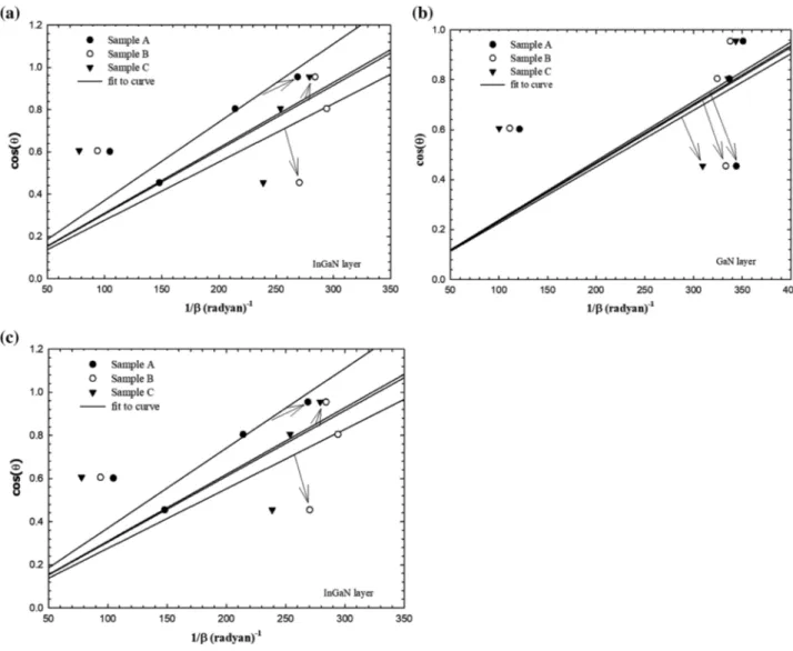
Here k is a constant, λ is the X-ray wavelength and θ is Bragg angle. By fitting the data, slope of the fit gives particle size
D. Using FWHM (βhkl) values gained from RSM, cosθ versus
(1) 𝛽hkl2 = 𝛽 2 S+ 𝛽 2 D. (2) D= k𝜆 𝛽hklcos 𝜃 → cos 𝜃 = k𝜆D ( 1 𝛽hkl ) .
1/βhkl Scherrer plot is drawn for InGaN active layer. This plot
can be seen in Fig. 5a. In Fig. 5b, c, Scherrer plots for GaN and AlGaN can be seen, respectively. By the slope of the fits in these plots D particle size is calculated in nm. According to these calculations, particle sizes for InGaN, AlGaN and GaN are found as 35.895, 21.773 and 51.326 nm, respectively. 3.2 Particle size calculation according to W–H
method
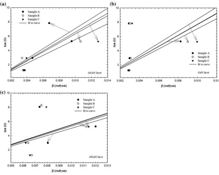
In reality not all the materials are crystalized. They mostly have deformation in their structures. Strain is a defect that comes out by the imperceptivity of the crystal or lattice mismatch. It can be calculated as ε ≈ βs/4tanθ. In the diffraction pattern, displacement of the peak causes variation in FWHM. For cal-culation of strain, it is thought as a linear equation as y = a × x. Tanθ versus βhkl line is plotted. When this plot is fitted slope
gives us 1/ε. Inverse of this expression mathematically gives
Fig. 5 a Scherrer plot (βhkl−1/cosθ) of InGaN layers for samples A, B and C. b Scherrer plot (βhkl−1/cosθ) of GaN layers for samples A, B and C. c Scherrer plot (βhkl−1/cosθ) of AlGaN layers for samples A, B and C
strain. This result is also not as realistic as in particle size calculation. However, W–H method is a technique that distin-guishes these two effects and it is compatible with the experi-mental method. It is useful to mention three methods used as W–H method. In this study W–H calculations are made according to three models. They are: uniform deformation model (UDM), uniform stress deformation model (USDM) and uniform deformation energy density model (UDEDM), respectively. W–H model is not dependent on 1/cosθ as in Scherrer model but it changes with Tanθ. This basic difference is used for distinguishing micro-strain and reflection broaden-ing [17]. Strain is caused from imperceptivity of the crystal and separation. It can be calculated with Eq. (3) [18]. Here ε is the square root of the mean square (RMS) value:
Figure 6a–c shows tanθ versus βhkl plots for InGaN, GaN
and AlGaN layers, respectively.
(3)
𝜀= 𝛽hkl 4 tan 𝜃.
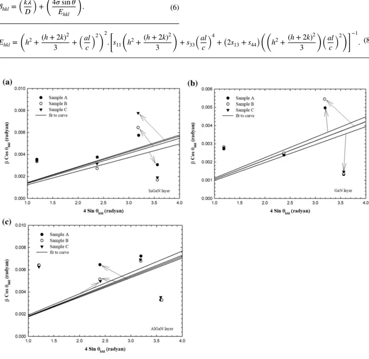
Strain and particle size are not independent of each other linearly. For this reason, peak width of Bragg reflections is given as the sum of the peak widths coming from two effects. Contribution of particle size and strain to line broadening are thought as independent of each other and by assuming that they both have a Cauchy-like profile, line width is the sum of two terms. This is given in the following equations:
This equation is known as classical W–H equation or uni-form deuni-formation model (UDM). According to this equation strain is the same in all directions. For this reason crystal is thought to be isotropic. On the other hand UDM is not dependent on direction. If βhklcosθhkl versus 4sinθhkl is
plot-ted using the miller planes of the crystal, slope gives the micro-strain ε. Intercept of y-axis gives the particle size. Calculated values are given in Tables 3, 4 and 5. For all three samples plots are given in Fig. 7a–c.
(4)
𝛽hkl= 𝛽1+ 𝛽𝜀=[K𝜆∕t cos 𝜃hkl] + [4𝜀 tan 𝜃hkl],
(5)
𝛽hklcos 𝜃hkl= 𝛽1+ 𝛽𝜀=[K𝜆∕t] + [4𝜀Sin𝜃hkl].
Because of the produced high pressure, diffraction line broadens and makes a shift to a bigger d space. This shows the stress in InGaN lattice. Positive strain value gained from
βhklcosθhkl versus 4sinθhkl plot supports the presence of stress. In
many situations, acceptation of homogeneity and isotropy is not true. For this reason, USDM and UDEDM methods are better methods because they take into account of Young modules [19].
According to USDM method, the reason for anisotropic micro-strain (εhkl) is uniform deformation stress (σ). Hooke’s
law related with strain describes the direct proportion between stress and strain as σ = εEhkl. Using this
approxi-mation W–H equation can be written as Eq. (6) [16]: (6) 𝛽hkl= (k𝜆 D ) + ( 4𝜎 sin 𝜃 Ehkl ) .
Here Ehkl is the Young modulus which is normal to the hkl
planes. Stress can be found by the slope of the 4sinθ/Ehkl
versus βhklcosθ plot. Particle size can be determined by the
interception point of the fit of this plot [17].
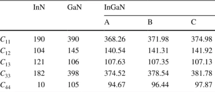
Elastic parameters of InN and GaN found in InGaN com-pound are given in Table 1. Elastic coefficients of InGaN can be calculated using Vegard’s law. Samples A, B and C have in ratios of 0.109, 0.090 and 0.080, respectively. Vegard’s law is given as
Young modulus for a hexagonal shaped crystal is given as [20, 21]:
(7)
c0(InGaN) = x c0(InN) + (1 − x) c0(GaN).
(8) Ehkl= ( h2+(h + 2k) 2 3 + (al c )2) 2 . [ s11 ( h2+(h + 2k) 2 3 ) + s33 (al c )4 +(2s13+ s44 ) (( h2+(h + 2k) 2 3 ) (al c )2)]−1 .
Fig. 7 a InGaN layers βhklcosθhkl versus 4sinθhkl plots. b GaN layers βhklcosθhkl versus 4sinθhkl plots. c AlGaN layers βhklcosθhkl versus 4sinθhkl
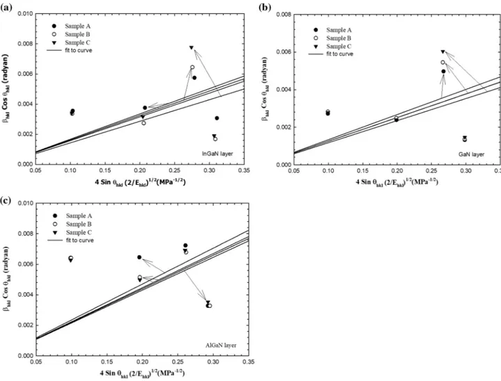
Here s11, s12, s13, s33, and s44 are elastic coefficients for InGaN and AlGaN, and they are given in Table 2.
Figure 8a–c shows βhklcosθhkl versus 4sinθhkl/Ehkl plots
for all three samples for InGaN, AlGaN and GaN according to USDM method.
Another model in W–H is USDEM. According to this model, the reason for strain is the deformation energy den-sity. According to Hooke’s law, u is the energy density as a
Table 1 Universal elastic coefficients of InGaN for all three samples
InN GaN InGaN
A B C C11 190 390 368.26 371.98 374.98 C12 104 145 140.54 141.31 141.92 C13 121 106 107.63 107.35 107.13 C33 182 398 374.52 378.54 381.78 C44 10 105 94.67 96.44 97.87
Table 2 Elastic compliances for
InGaN and AlGaN (Gpa−1) A B C
InGaN AlGaN InGaN AlGaN InGaN AlGaN
S11 0.0033 0.0030 0.0033 0.0030 0.0032 0.0030
S12 0.0011 0.0010 0.0011 0.0010 0.0011 0.0010
S13 0.0006 0.0005 0.0006 0.0005 0.0006 0.0005
S33 0.0030 0.0028 0.0030 0.0028 0.0030 0.0028
S44 0.0106 0.0086 0.0104 0.0087 0.0102 0.0086
Fig. 8 a βhklcosθhkl versus 4sinθhkl/Ehkl plots for InGaN layers according to USDM model. b βhklcosθhkl versus 4sinθhkl/Ehkl plots for GaN layers
function of strain. It may be given as u = ε2E
hkl/2. So Eq. (6)
can be modified [17]
Figure 9a–c shows βhklcosθhkl versus 4sinθ(2u/Ehkl)1/2
plots for InGaN, AlGaN and GaN, respectively. If these plots are fitted, the slope of the fit gives anisotropic energy density (u) and y-axis intercept gives particle size (D). Deformation stress and deformation energy density can be related with each other as u = σ2/2E
hkl in USDM and UDEDM models
[17]. Equations (7) and (8) are different because they take into account the anisotropic elastic coefficients. In Eq. (7), deformation stress is the same in all directions and this situ-ation makes u anisotropic.
In Eq. (8), deformation energy is accepted as uniform in all directions. Here deformation stress σ is taken as (9) 𝛽hkl= (k𝜆 D ) + ( 4 sin 𝜃 ( 2u Ehkl )1∕2) .
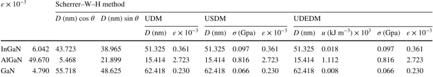
anisotropic. For this reason, different values for strain and particle size can be found from these two equations. In Tables 3, 4 and 5, results gained from UDM, USDM and UDEDM, and Scherrer are listed for InGaN, AlGaN and GaN layers of samples.
Results showed that strain is less effective on particle size [22]. If Tables 3, 4 and 5 are examined carefully, par-ticle sizes gained from Scherrer and W–H can be com-pared. On the other hand, UDM, USDM and UDEDM methods gave similar results because the three methods are based on the W–H method. Young’s modulus results from the harmony between Hoke’s Law and anisotropic energy density. The same results were obtained because the a- and
c-lattice parameters were used in the Young module. Strain
in big angles results in the broadening of the peaks and particle size decrease. This situation is caused by increas-ing of reflection angles [22].
Fig. 9 a βhklcosθhkl versus 4sinθ(2u/Ehkl)1/2 plots for InGaN layers according to UDEDM model. b βhklcosθhkl versus 4sinθ(2u/Ehkl)1/2 plots for
3.3 Morphological properties of InGaN/GaN MQW blue LEDs
The morphological properties of the surface were char-acterized by high-performance Nano magnetic Pro-AFM atomic force microscopy (AFM) in dynamic scanning mode. Table 6 gives surface roughness values for three samples. Figure 10a–c shows a 3D AFM image of samples A, B and C at a scanning area of 5 × 5 µm2 at 650, 667 and 700 °C, respectively. Table 6 gives the surface roughness values for three samples. If the shape is carefully examined for sample A, cylindrical island formation is clearly visible. The B sam-ple has better surface morphology than the other samsam-ples
and is more homogeneous. Furthermore, the B sample has large particle shapes instead of cylindrical islands. Sample C consists of cylindrical islands as in sample A and has more surface roughness compared to sample B.
Variation of particle size is related with RMS value variations. These results are in accordance with the results gained from W–H. Also, surface morphology of samples A, B and C are like GaN structures grown by MOCVD in literature [21]. AFM results showed that surface morphol-ogy of InGaN/GaN LED structures is strongly affected by the growth temperature.
4 Conclusion
In this study, three samples of InGaN/GaN LED structures are grown by MOCVD method at 650, 667 and 700 °C active layer growth temperatures. These structures are character-ized by HR-XRD method. Different from classical HR-XRD method, reciprocal space mapping technique is used. Using
Table 3 Physical parameters calculated for all three layers of sample A according to USD, USDM and UDEDM models ε × 10−3 Scherrer–W–H method
D (nm) cos θ D (nm) sin θ UDM USDM UDEDM
D (nm) ε × 10−3 D (nm) σ (Gpa) ε × 10−3 D (nm) u (kJm−3) × 103 σ (Gpa) ε × 10−3
InGaN 7.334 36.087 35.895 47.542 0.250 47.542 0.066 0.250 47.542 0.008 0.066 0.250
AlGaN 36.872 7.366 21.773 14.031 2.997 14.031 0.900 2.997 14.031 1.348 0.900 2.997
GaN 4.351 61.232 51.326 57.597 0.021 57.597 0.006 0.021 57.597 0.000 0.006 0.021
Table 4 Physical parameters calculated for all three layers of sample B according to USD, USDM and UDEDM models
ε × 10−3 Scherrer–W–H method
D (nm) cos θ D (nm) sin θ UDM USDM UDEDM
D (nm) ε × 10−3 D (nm) σ (Gpa) ε × 10−3 D (nm) u (kJm−3) × 103 σ (Gpa) ε × 10−3
InGaN 6.123 48.362 41.134 48.947 0.104 48.947 0.028 0.104 48.947 0.001 0.028 0.104
AlGaN 42.704 6.319 21.780 15.019 2.815 15.019 0.838 2.815 15.019 1.180 0.838 2.815
GaN 4.555 58.651 49.270 56.266 0.066 56.266 0.019 0.066 56.266 0.001 0.019 0.066
Table 5 Physical parameters calculated for all three layers of sample C according to USD, USDM and UDEDM models ε × 10−3 Scherrer–W–H method
D (nm) cos θ D (nm) sin θ UDM USDM UDEDM
D (nm) ε × 10−3 D (nm) σ (Gpa) ε × 10−3 D (nm) u (kJ m−3) × 103 σ (Gpa) ε × 10−3
InGaN 6.042 43.723 38.965 51.325 0.361 51.325 0.097 0.361 51.325 0.018 0.097 0.361
AlGaN 49.670 5.468 21.899 15.414 2.723 15.414 0.816 2.723 15.414 1.112 0.816 2.723
GaN 4.790 55.718 48.625 62.418 0.230 62.418 0.066 0.230 62.418 0.008 0.066 0.230
Table 6 Surface roughness
values for three samples Sample RMS (nm)
A 2.07
B 9.55
Fig. 10 a 3D AFM image of
sample A. b 3D AFM image of sample B. c 3D AFM image of sample C
this technique, mixed InGaN, AlGaN and GaN peaks are determined more clearly and βhkl values are determined with
better accuracy. With the increase of the temperature in the plane 106, the relaxation status of the InGaN from the RSM for the three samples created a strain in the “l” direction. While the inverse space points of AlGaN and GaN coincide, the crystallinity of the increased temperature is distorted in the “l” direction.
In direction 004, the orientation of AlGaN in the “l” direction is clearly seen with increasing temperature. InGaN’s “l” direction shows increased strain in FWHM. βhkl
values gained from reciprocal space mapping and universal elastic coefficients of the material are used in W–H method to determine particle size (D), uniform stress σ (GPa), strain
ε and anisotropic energy density u (kJ m−3). The results for these parameters are compared with literature.
As the result of the calculations, according to Scher-rer method, InGaN particle size values first increase and later decrease with increasing temperature. The same value decreases continuously for AlGaN and GaN. Particle size values gained from UDM, USDM and UDEDM are very near to each other. Strain values are found the same in all three methods. For InGaN layer, it first increases and later decreases, for AlGaN layer it decreases and for GaN layer it increases with an increase in temperature. Uniform stress values presented the same behavior as the strain for each three layers. Anisotropic energy density values showed decreasing later increasing behavior for InGaN, continuously decreasing for AlGaN, and increasing for GaN layers with an increase in temperature. The increase in anisotropic energy density for InGaN and GaN, and the decrease in AlGaN is due to the increase of the stress values along with the temperature.
On the other hand according to Scherrer method for InGaN layer in sample A, results gained for sinθ are 0.5% smaller than for cosθ. The same comparison is 15% for sample B and 11% for sample C. In GaN layer similar behaviors are noticed as InGaN. For InGaN layer val-ues are three or four times larger than the others. This
increase in values is proportional with growth tempera-ture. Broadening of lines in HR-XRD is thought to be caused from particle size and lattice strain. All the results gained in this study are in good agreement with ones in literature. Especially, it is noticed that UDEDM method is the most suitable method for calculating strain and other parameters.
Acknowledgements This work was supported by the Presidency
Strategy and Budget Directorate (Grants Number 2016K121220).
References
1. H. Markoc, Hand book of nitride semiconductors and devices (Wiley-VCH, 2008), pp 76–78
2. Y. Bas, PhD thesis (University of Gazi, Turkey) (2015) 3. D. Kapolnek et al., App. Phys. Lett. 67, 11 (1995)
4. F.A. Ponce, B.S. Krusor, J.S. Major, W.E. Plano, D.F. Welch, Appl. Phys. Lett. 67, 3 (1995)
5. S. Chichibu, T. Azuhata, T. Sota, S. Nakamura, Appl. Phys. Lett.
69, 27 (1996)
6. S.D. Lester, F.A. Ponce, M.G. Craford, D.A. Steigerwald, Appl. Phys. Lett. 66, 10 (1995)
7. M. Schuster et al., J. Phys. D App. Phys. 32, 10a (1999) 8. S. Çörekçi et al., J. Mater. Sci. 46, 1606–1612 (2011) 9. P. Tasli et al., Cryst. Res. Technol. 45, 2 (2010)
10. D.D. Koleske et al. Solid State Lighting and Solar Energy Tech-nologies. (Society of Photo Optical, 2008), pp 17–40 11. M.K. Ozturk et al., J. Mater. Sci. Mater. Electron. 21, 2 (2010) 12. M.K. Ozturk et al., Strain 47 (2011)
13. C. Kisielowski, Semi. Semi. 57 (1999)
14. M.A. Moram, M.E. Vickers, Rep. Prog. Phys. 72 3 (2009) 15. Y. Bas et al., J. Mater. Sci. Mater. Electron. 25, 9 (2014) 16. M.K. Ozturk et al. Appl. Phys. A Mater. Sci. Proc. 114, 4
(2014)
17. G. Singla, K. Singh, O.P. Pandey, Appl. Phys. A Mater. Sci. Proc. 113, 1 (2013)
18. A.K. Zak, W.H.A. Majid, M.E. Abrishami, R. Yousefi, Sol. State Sci. 13, 1 (2011)
19. Y. Rosenberg et al., J. Phys. Con. Mat. 12, 37 (2000) 20. D. Balzar, H. Ledbetter, J. Appl. Crys. 26 (1993) 21. Z.F. Ma et al., J. Phys. D Appl. Phys. 41, 10 (2008) 22. M.K. Ozturk et al., Strain. 47, 19–27 (2011)