NOVEL CONCEPTS IN HIGH POWER
SEMICONDUCTOR LASERS
a dissertation submitted to
the graduate school of engineering and science
of bilkent university
in partial fulfillment of the requirements for
the degree of
doctor of philosophy
in
physics
By
Seval Arslan
November 2018
Novel concepts in high power semiconductor lasers By Seval Arslan
November 2018
We certify that we have read this dissertation and that in our opinion it is fully adequate, in scope and in quality, as a dissertation for the degree of Doctor of Philosophy.
O˘guz G¨ulseren(Advisor)
Atilla Aydınlı (Co-Advisor)
Ceyhun Bulutay
Ra¸sit Turan
Alpan Bek
Onur Tokel
Approved for the Graduate School of Engineering and Science:
Ezhan Kara¸san
ABSTRACT
NOVEL CONCEPTS IN HIGH POWER
SEMICONDUCTOR LASERS
Seval Arslan Ph.D. in Physics Advisor: O˘guz G¨ulseren Co-Advisor: Atilla Aydınlı
November 2018
This doctoral thesis deals with innovations to the cavity optics of high power semiconductor lasers emitting light at 9xx nm. High power laser diodes are com-plex electronic and photonic systems. Developments in epitaxial crystal growth techniques and the quality that ensued has been the driving force in the progress of the field. Semiconductor lasers with high output powers and high efficiencies have thus become possible. Commercial single emitters each with over 10 watts output with efficiencies reaching 60% is available.Even higher output powers have been demonstrated in the lab. High power semiconductor lasers have many ap-plications such as acting as optical pumps in other lasers, range finding, optical storage, light sources in sensors and medical tools. The demand for higher pow-ers and efficiencies continues. Among several possibilities, one of the main limits of maximum output power is the catastrophic optical mirror damage (COMD). At high pump currents and hence output powers, facet absorption leads to tem-peratures high enough to damage the cavity mirrors. This thesis is focused on novel approaches to increase the COMD threshold. We demonstrate design, fab-rication and characterization of the high power strained InGaAs/AlGaAs lasers emitting light at 9xx nm. To prevent facet absorption which decreases the laser efficiency especially at high injection currents, band gaps in the vicinity of the laser facet are increased using impurity-free vacancy disordering (IFVD) while preserving the band gap in the lasing region away from the facets. A record large bandgap at the facet region, relative to that of the lasing region is achieved by thermal stress management of a bilayer dielectric structure. We demonstrate ex-cellent optical loss and optical power output with this bilayer approach. Further, positive feedback cycle during absorption at the facets is broken by keeping the facets cold, by design. Thus, in this cold window approach, we extend the passive unpumped windows to keep the heat source from the main body of the cavity away from the facets while eliminating the additional loss incurred by biasing
iv
this section to transparency. This new biased window approach leads to much cooler facet temperatures while reducing the bulk temperatures as well. Thus, we use thermoreflectance spectroscopy to measure facet temperature as a function of pump and bias current. We clearly demonstrate that, for the first time, facet temperatures have been decreased below the bulk temperature without penalty on the output power.
¨
OZET
Y ¨
UKSEK G ¨
UC
¸ L ¨
U YARI˙ILETKEN LAZERLERDE YEN˙I
KAVRAMLAR
Seval Arslan Fizik B¨ol¨um¨u, Doktora Tez Danı¸smanı: O˘guz G¨ulseren ˙Ikinci Tez Danı¸smanı: Atilla Aydınlı
Kasım 2018
Bu doktora tezi, 9xx nm’de ı¸sık yayan y¨uksek g¨u¸cl¨u yarıiletken lazerlerinin kovuk optiklerine y¨onelik yeniliklerle ilgilidir. Y¨uksek g¨u¸cl¨u lazer diyotları karma¸sık elektronik ve fotonik sistemlerdir. Kristal b¨uy¨utme tekniklerindeki geli¸smeler ve ortaya ¸cıkan y¨uksek kalitedeki epitaksiyel kristaller, alanın iler-leyi¸sinde itici g¨u¸c olmu¸stur. Bu kristallerle yapılan lazerler y¨uksek g¨u¸c ve y¨uksek verim g¨ostermektedirler. Ticari olarak satılan tek emit¨orlerin her birinden 10 Watt’ın ¨uzerinde y¨uksek ¸cıkı¸s g¨uc¨u ve %60’a varan verimlilikler g¨osterilmi¸stir. Laboratuvarlarda daha y¨uksek g¨u¸cler de elde edilmi¸stir.
Y¨uksek g¨u¸cl¨u yarıiletken lazerler, di˘ger lazerlerde optik pompalar, teleme-tre bulma, optik depolama, sens¨orlerde ı¸sık kaynakları ve medikal aletler gibi bir¸cok uygulamaya sahiptir. Daha y¨uksek g¨u¸c ve verimlilik talebi devam ediyor. Birka¸c olasılık arasında, maksimum ¸cıkı¸s g¨uc¨un¨un ana limitlerinden biri katas-trofik optik ayna hasarıdır (COMD). Y¨uksek pompa akımlarında ve dolayısıyla ¸cıkı¸s g¨u¸clerinde faset so˘gurması, kovuk aynalarına zarar verebilecek kadar y¨uksek sıcaklıklara yol a¸car. Bu tez, COMD e¸si˘gini artırmak i¸cin yeni yakla¸sımlara odaklanmı¸stır. Nitekim, bu tezde 9xx nm’de ı¸sık yayan y¨uksek g¨u¸cl¨u ger-ilmi¸s InGaAs / AlGaAs lazerlerinin tasarımı, ¨uretimi ve karakterizasyonunu g¨ostermekteyiz. Lazer verimlili˘gini ¨ozellikle y¨uksek enjeksiyon akımlarında azal-tan faset so˘gurmasını ¨onlemek i¸cin, ı¸sıma b¨olgesinde korunurken, lazer fase-tinin ¸cevresindeki yasak bant aralı˘gı safsızlıksız atomları kullanmaksızın bo¸sluk d¨uzensizli˘gi (IFVD) kullanılarak arttırılır. ˙Iki b¨olgeli bir dielektrik yapının ısıl stres y¨onetimi ile faset b¨olgesinde, ı¸sıma b¨olgesine g¨ore varolan en y¨uksek bant aralı˘gı elde edilir.Bu iki katmanlı yakla¸sımla m¨ukemmel optik kayıp ve optik g¨u¸c ¸cıkı¸sı g¨osteririz. Ayrıca, fasetlerde so˘gurma sırasında olumlu geribildirim d¨ong¨us¨u, fasetleri tasarımla so˘guk tutarak kırılır. Bu nedenle, bu so˘guk pencere
vi
yakla¸sımında, ısı kayna˘gını kovu˘gun ana g¨ovdesinden uzak tutmak i¸cin pasif pom-palanmamı¸s pencereleri uzatıp, bu b¨ol¨um¨un ge¸cirgen hale getirerek meydana gelen ek kayıpları ortadan kaldırıyoruz.Bu yeni ileri besleme altındaki pencere yakla¸sımı, yı˘gın sıcaklıklarını da azaltırken ¸cok daha d¨u¸s¨uk faset sıcaklıklarına yol a¸car. B¨oylece, pompa ve ileri besleme akımının bir fonksiyonu olarak faset sıcaklı˘gını ¨ol¸cmek i¸cin termoyansıma (thermoreflectance) spektroskopisini kul-lanıyoruz. ˙Ilk kez, ¸cıkı¸s sıcaklıklarında d¨u¸s¨u¸s olmadan faset sıcaklıklarının k¨utle sıcaklı˘gının altına d¨u¸st¨u˘g¨un¨u a¸cık¸ca g¨osterdik.
Acknowledgement
First of all, I would like to express my special thanks to Prof. Dr. Atilla Aydınlı for giving me a chance to carry out my Ph.D. on laser diodes. He has extensive knowledge and experience of semiconductors and has always tried to convey them to me. With his valued advice, he gave me the courage to accomplish the tough work.
I am sincerely grateful to my advisor and the head of the Department of Physics, Prof. Dr. O˘guz G¨ulseren for his support during my Ph.D.
I would like to thank Prof. Dr. Ceyhun Bulutay, Prof. Dr. Ra¸sit Turan, Assoc. Prof. Dr. Alpan Bek and Asst. Prof. Dr. Onur Tokel for reviewing my thesis and sharing their valuable comments.
It is a pleasure to acknowledge Dr. Abdullah Demir for permanent availability for scientific discussions. I am grateful for his support during my studies with his practical ideas.
My warm gratitude belongs to Sinan G¨undo˘gdu for the supporting me during many aspects of laser testing and analysis. He also provided a very fruitful discussion environment. Hard times got cheerful thanks to his friendship.
I would like to warmly thank my dear friend Seval S¸ahin for her support in laser processing. Besides the help in laboratory work, my good friend Seval always made me feel special.
I would like take this opportunity to thank my friends, Ali Murat S¨ozen, Rahim Bahari, Berk Berkan Turgut, Muhammet Gen¸c, Seda Arpacı, Mustafa El¸ci, Fatih Bilge Atar, Do˘gukan Apaydın and Enes Seker for a warm and cheerful. atmosphere.
I sincerely thank Murat G¨ure and Erg¨un Karaman and Elvan ¨O˘g¨un for their constant administrative and technical support.
I would like to acknowledge financial support of ERMAKSAN A. S¸. which made this study possible.
A very special word of thanks goes to my parents. They have always encour-aged me to finish my doctorate in the best way possible. I am grateful to both for a lifetime of support and love.
viii
during the Ph.D. years. He has been very patient and made me feel special by showing how proud he is with me. Thank you honey.
Contents
1 Introduction 1
2 Fundamentals of diode lasers 7
2.1 Basic diode laser concept . . . 7
2.2 Laser operating model . . . 11
2.2.1 Carrier injection and photon generation . . . 11
2.2.2 Optical loss, gain and threshold conditions . . . 13
2.2.3 Current dependent optical output characteristics . . . 14
2.3 Thermal characteristics of the high power diode lasers . . . 17
2.3.1 Characteristic temperatures and thermal resistance . . . . 17
2.3.2 Theory of the catastrophic mirror damage . . . 18
2.4 Fast axis and slow axis beam divergence . . . 19
3 Experimental 22 3.1 Design of a high power diode laser . . . 22
3.1.1 Electronic design . . . 23
3.1.2 Optical design . . . 24
3.1.3 Crystal growth . . . 25
3.2 Micro-fabrication of edge emitting broad area diode lasers . . . . 27
3.3 Mounting of high power lasers for testing . . . 28
3.4 Characterization techniques . . . 31
3.4.1 L-I-V characteristics and optical spectrum analysis . . . . 31
3.4.2 Internal loss and internal efficiency analysis . . . 34
CONTENTS x
3.4.4 Thermo-reflectance method for facet temperature measure-ments . . . 40
4 Novel concepts for cavity optics 45 4.1 Cavities with cold windows . . . 47 4.1.1 Fabrication of biased window high power diode lasers . . . 47 4.1.2 L-I-V measurement of biased window high power diode lasers 49 4.1.3 Facet temperature measurements . . . 52 4.1.4 Simulation of facet temperature rise . . . 55 4.2 Selective band gap engineering . . . 59 4.2.1 Photoluminescence measurements of the band gap shift . . 61 4.2.2 Fabrication of lasers with IFVD . . . 76 4.2.3 Spectrum of lasers . . . 78 4.2.4 L-I-V measurements of lasers with IFVD . . . 79
List of Figures
2.1 The schematic illustration of the Fabry-Perot resonator . . . 8 2.2 Schematic illustration of the energy band diagram versus vertical
direction x for the forward biased double heterostructure. . . 10 2.3 Schematic illustrations of (a) gain guided laser (b) ridge waveguide
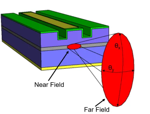
laser and (c) buried heterostructure. . . 11 2.4 Schematic representation of the near and far field profiles of the
ridge waveguide laser. . . 20
3.1 Laser structure. . . 23 3.2 Calculated mode profile of the laser. . . 24 3.3 Schematic illustrations of the (a) MBE and (b) MOCVD systems
(Figures reprinted from . . . 26 3.4 Laser diode chip fabrication steps. . . 28 3.5 The optical microscopy images from the top surface of the 3.00 mm
long fabricated lasers with three different widths of 50, 100 and 200 µm after (a) mesa etch, (b) Si3N4 removal from the contact region,
(c) lift-off and (d) electroplating. . . 29 3.6 Pick and place instrument. . . 30 3.7 a) Wedge bonder and b) mounted and wire bonded laser chip. . . 30 3.8 Schematics of the a) pulsed and b) CW measurement set-ups. . . 31 3.9 L-I measurements of 3.00, 4.00 and 5.00 mm long lasers under (a)
pulsed and (b) CW operations. . . 32 3.10 The L-V and PCE as a function of operating current for the 4.00
LIST OF FIGURES xii
3.11 The optical spectra of the 4.00 mm long broad area laser for differ-ent CW operation currdiffer-ents. Inset represdiffer-ents the spectral line width and wavelength of this laser as a function of operation current. . . 34 3.12 Inverse external differential efficiency versus cavity length. . . 35 3.13 The threshold current density as a function of inverse cavity length
(Copyright 2018 IEEE . . . 36 3.14 Schematic illustration of the lateral and vertical far-field
charac-terization set-up. a) Laser diode b) first galvo mirror c) second galvo mirror d) photo diode. . . 38 3.15 Beam profile of 100 µm width and 4.00 mm long laser under 3A
CW operation current. . . 39 3.16 (a) The vertical and (b) lateral beam profile of 100 µm width 4.00
mm long laser under 3A CW operation current. . . 40 3.17 Schematic of the thermoreflectance measurement set-up (redrawn
from . . . 41 3.18 The proportionality constant of thermoreflectance. . . 42 3.19 The temperature map for different time interval of the laser pulse. 42 3.20 The temperature map of 5.00 mm long conventional laser at 4.00
A and (b) The temperature line scan for 5.00 mm long laser taken at the active region through the direction perpendicular to surface. 43 3.21 (a) Wavelength versus laser temperature and (b) dissipated power
versus wavelength. . . 44
4.1 The optical microscopy images from the top surface of the biased window high power diode laser after (a) ridge waveguide etch, (b) Si3N4 removal from the contact regions (c) lift-off and (d)
electro-plating. . . 48 4.2 The line graph of voltage versus current between the lasing and
window region of 4.00+ 1.00 mm long biased window laser. . . 49 4.3 The front facet output power at various injection currents for lasers
with and without 1.00 mm long window region (window current is at 170 mA). Schematic illustrations of the two different laser designs are also shown (Copyright 2018 IEEE . . . 50
LIST OF FIGURES xiii
4.4 The threshold currents and the slope efficiencies of the 4.00 mm and 5.00 mm long standard lasers and biased window lasers for various biasing currents (Copyright 2018 SPIE . . . 51 4.5 The temperature maps of (a-c) 5.00 mm long standard laser, 4.00+
1.00 mm and 4.25+ 0.75 mm long lasers, respectively and (d) the comparison of the temperature profiles obtained from the map of these lasers at 5A (Copyright 2018 IEEE . . . 53 4.6 The facet temperature rise of 5.00 mm long standard laser and
4.00+ 1.00 mm long biased window lasers as a function of bias current for various pump currents of 1A, 3A and 5A. Bulk temper-ature rise of standard laser is also shown for these pump currents (Copyright 2018 IEEE . . . 54 4.7 (a) Schematic illustration of the COMSOL model. . . 56 4.8 The active region temperature change of 4.00 mm long biased
win-dow laser with various winwin-dow length of 500, 1000, 1500 and 2000 µm through the laser cavity. Inset shows the top temperature map of the biased window laser with 1000 µm window length. . . 57 4.9 (a)The active region temperature change of 4.00 mm long biased
window laser with (a) 12.8 K/W (b) 2.5 K/W thermal resistance as a function of window length for various dissipated power of 5W, 10W, 15W and 20W. . . 58 4.10 Schematic illustration of the IFVD process. . . 59 4.11 An example for the ellipsometer model and model parameters used
to analyze the thickness and the optical properties of the SixO2
and the measurement and fit profiles of the Ψ and ∆ are given. Also, refractive index profiles obtained from the fit is shown. . . . 63 4.12 Intermixing and suppression configuration used for comparison of
PL wavelength shift of 250 nm SiO2, SrF2 and SixO2. . . 64
4.13 The normalized PL spectra of the as-grown and SrF2, SixO2, SrF2
capped samples under RTA annealing condition of 880◦C for 2 minutes (Copyright 2018 IOP . . . 66 4.14 PL peak wavelength shifts under RTA annealing conditions of 860
LIST OF FIGURES xiv
4.15 The optical microscopy images of a) SiO2, b) SixO2and c) SrF2film
covered surfaces, respectively, obtained from the sample surfaces after the removal of dielectric films (Copyright 2018 IOP . . . 68 4.16 The optical microscopy images of SrF2 surfaces (a) after film
de-position (b) after RTP process of the sample. . . 68 4.17 Bilayer configuration to decrease thermal stress. . . 69 4.18 The comparison of the optical microscopy and AFM measurement
results of the SixO2: SrF2 and SrF2 capped samples after dielectric
film etch process (Copyright 2018 IOP . . . 70 4.19 The normalized PL spectra of as-grown and SiO2: SixO2: SrF2
and SixO2: SrF2 capped samples annealed at 880 ◦C for 2 min.
(Copyright 2018 IOP . . . 72 4.20 The PL peak wavelength shift of SiO2: SixO2: SrF2, SixO2, SixO2:
SrF2 and SrF2 capped samples annealed at various temperatures
of 860, 880, 900 and 920◦C (Copyright 2018 IOP . . . 73 4.21 (a) The FWHM and (b) integrated PL intensity of SiO2: SixO2:
SrF2 and SixO2: SrF2 capped samples annealed at 880 ◦C for 2
min. (Copyright 2018 SPIE . . . 74 4.22 The normalized PL spectra of SiO2: SixO2: SrF2 and SixO2: SrF2
capped regions after RTA process at 880◦C for 6 min. compared to as-grown structure (Copyright 2018 IOP . . . 75 4.23 PL peak wavelength shift under annealing conditions of 2 to 8 min.
at 880◦C (Copyright 2018 IOP . . . 75 4.24 The FWHM and integrated PL intensity of intermixed and
sup-pressed regions at 880◦C from 2 to 6 min. (Copyright 2018 SPIE 76 4.25 The optical microscopy images of the lasers after (a) cap layer
removal (b) dielectric film deposition (c) Si3N4 removal from the
contact regions and (d) electroplating. . . 77 4.26 The normalized PL and lasing spectra of the SixO2: SrF2 capped
suppression and SiO2 capped intermixing lasers as a results of
LIST OF FIGURES xv
4.27 The CW output power of the SiO2, SrF2, SixO2: SrF2 and
as-grown lasers. Inset shows the threshold currents of these lasers (Copyright 2018 IOP . . . 80 4.28 Inverse external differential quantum efficiency of the SixO2: SrF2
and as-grown lasers as a function of cavity length (Copyright 2018 IOP . . . 81
List of Tables
4.1 Refractive index analysis of PECVD deposited SiO2 and SixO2 . . 64
4.2 The thermal stress of various materials and the physical parameters used to calculate stress (Copyright 2018 IOP . . . 69 4.3 Threshold current, slope efficiency and differential quantum
Chapter 1
Introduction
The word laser (light amplification by stimulated emission of radiation) was first used by Gordon Gould and experimentally demonstrated by Theodore Maiman in 1960 [1]. In contrast with the ruby laser of Maiman, semiconductor diode lasers are electrically pumped solid state lasers and they are highly preferred for many applications such as communications, material processing, medical, lithography due to their compactness and higher efficiency compared to the other types of lasers. Diode laser technology accelerated after the development of metal organic chemical vapor deposition (MOCVD) and molecular beam epitaxy (MBE) crystal growth technologies which allow the deposition of semiconductors with different compositions on top of one another. The ability to grow many different compo-sitions and thicknesses can be exploited to engineer the band gap of each layer and build novel devices [1, 2].
Laser performance is evaluated in terms of wavelength tunability, diffraction limited high beam quality, high optical output power and long term reliability. These operational characteristics of laser diodes are based on the electronic and optical design as well as suitable fabrication technology and high quality crystal growth. Laser diodes are characterized by voltage-current-optical output power measurements. Bias voltage injects electrical carriers into the laser making it necessary to understand their transport. In response to the injected current,
coherent photons are generated by recombination in the presence of optical fields, which points to the necessity of understanding the optical fields inside the cavity.
The emission wavelength of the band to band recombination lasers depends on the band-gap of the active region material [3, 2]. In the case of lasers that depend on quantum well(s) for the emitted light, emission wavelength is deter-mined by the lowest bound states in the conduction and valence bands of the quantum well(s).The material system of a semiconductor laser should consist of layers that are lattice matched for defect free laser epitaxy since defects are non-radiative recombination centers decreasing the laser’s internal quantum efficiency. However, the laser emission wavelength in the range of 900-1100 nm in the Al-GaAs/InGaAs quantum well structures can not be covered by a lattice matched layer system. This range of emission can be covered by the strained-layer system of InxGa1−xAs/AlyGa1−yAs or InxGa1−xAs/GaAs epitaxy by adjusting the
thick-ness and composition of the InGaAs quantum well. [2, 4]. The misfit locations that may arise in these strained layer systems do not have significant detrimental effects on laser performance [2].
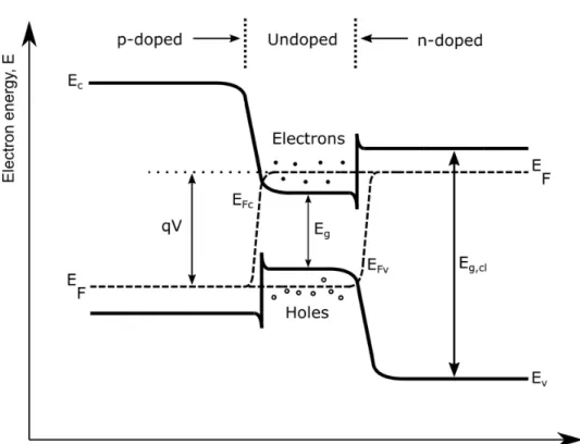
The electro-optical design which determines the emission wavelength as well as the transverse lateral and the vertical confinement, affects the efficiency of high power diode lasers. The first diode lasers had a homo-junction design. A homo-junction consists of n- and p- doping of the same semiconductor material. However, the threshold of the homo-junction lasers are very high due to the low mode overlap between the active region and mode. In these lasers there is no mode confinement in the transverse direction, therefore the mode spreads into the highly doped claddings leading to free carrier absorption. Hence, the effi-ciency of the homo-junction lasers is very low and it works under pulsed bias due to heating problems. The double heterostructure diode lasers show better performance compared to the homo-junction lasers. As the name implies, double heterostructure consists of thin layers of smaller bandgap (higher index) semicon-ductor material sandwiched between the thicker n- and p- type larger bandgap (lower index) semiconductor materials. The active layer thickness in these lasers are typically is in the range of 0.1 to 0.2 µm [2]. These structures enable car-rier confinement in the thin active layer under forward bias conditions, which
force the carriers to recombine in the active region. Furthermore, the index dif-ference between the active layer and the cladding provides mode confinement in the active layer, hence the mode overlap with active layer increases, and the gain threshold decreases. In addition, mode confinement prevents mode spread-ing into the claddspread-ing layers. Thus, absorption loss due to free carriers in the doped cladding layers is eliminated. As a result, the threshold current density is much lower compared to that of the homo-junction lasers. When the active layer thickness is reduced, the carrier confinement and mode overlap decreases leading to an increase in the threshold. However, very thin active layers with thicknesses in the range of de Broglie wavelength shows quantum size effects, and single or multi quantum well (QW) laser performs significantly improved re-sults. The staircase like density of electronic states instead of parabolic density of states as in the double-heterostructures and small active volume are the rea-sons for the low threshold current density of QW lasers. The difference between the density of states of the bulk and QW material changes the gain curve. The gain curve of bulk material is wide and highly energy dependent whereas QW lasers have narrow gain curves due to the high density of states around ground states. As a result, lower number of carriers are needed for population inversion and the spectral shift due to the band filling effect is very low compared to the bulk material. To increase the carrier and photon confinement in QW lasers, the graded refractive index separate-confinement heterostructure (GRIN-SCH) is used. GRIN-SCH structure consists of single or multiple QWs sandwiched between the graded lower index and higher bandgap semiconductor surrounded yet by lower index and higher bandgap cladding. This approach provides carriers confinement in QW and mode confinement within the SCH region which prevents the free carrier absorption loss due to the highly doped cladding layers.
For the edge emitting diode lasers, transverse lateral current and photon con-finement can be achieved by weak index guiding mechanism as in the ridge waveg-uide lasers. Ridge is formed by etching the laser structure down to the cladding layer and deposition of a dielectric layer next to the edge of the ridge prevent current loss through leakage. Photons are confined in the lateral direction due
to the index step. The lateral single mode operation is crucial for many ap-plications. Therefore, the ridge width and height, and active region thickness should be carefully adjusted for single mode operation. Narrow ridge waveguide lasers are highly preferred for many applications because of low optical losses and thresholds, ease of fabrication and high optical output power in single lateral mode.
Generally speaking, the laser’s with an output power larger than 1W is labeled as high power diode lasers [2]. Increasing the output power of semiconductor diode lasers have opened up new application areas such as optical fiber amplifier pumping and material processing which also necessitates the improvement of laser performance. The main factors that limit power output of semiconductor lasers are carrier leakage, gain saturation leading to spatial hole burning (SHB), free carrier absorption, catastrophic optical damage (COD) and catastrophic optical mirror damage (COMD) [5, 6, 7]. There are two reasons for the carrier leakage. First, is the carrier overflow from the active layer. Carriers diffuse without being captured by the quantum well(s) due to the finite diffusion time of the carriers. This effect can be seen even at threshold and increases with current [8]. Second, is the finite relaxation time of the carriers in the quantum well(s) [9]. Electrons and holes leak to the waveguide from the quantum well without contributing to the stimulated recombination. Carrier leakage leads to optical losses via radiative or non-radiative recombination. It can be reduced using the MQWs in the active region [7, 10] as well as eletcron or hole barriers strategically placed in the active region. Spatial hole burning becomes dominant under high power densities. In this condition, the stimulated emission due to the high photon density reduces the local gain because it removes the carriers contributing to the gain. The spatial hole burning (SHB) is a complicated phenomenon and has been studied by many researchers in more detail in refs [11, 12]. This effect can be minimized by reducing confinement factor with vertical designs [7]. COMD and COD are irreversable processes which occur on the laser facets and in the bulk of the laser cavity due to the strong heating caused by high optical power density and non-radiative recombination. Optical power density can be reduced by reducing the mode confinement factor. COMD threshold can also be increased by making
proper surface passivation of the facets or using quantum well intermixing (QWI) techniques. Surface passivation aims to reduce or stabilize the surface states against thermodynamically unstable species such as arsenic, arsenic oxides and adsorbed water [13]. QWI is used to increase the bandgap in the proximity of the laser facet while keeping the rest of the cavity at the original band gap. Increasing the band gap decreases the facet absorption and facet temperature. However, there has, so far, been no way to decrease facet temperature below the bulk temperature.
This thesis concentrates on novel approaches to increase reliable optical output power from InGaAs based high power laser diodes. It covers three main sections; In the Chapter on fundamentals of diode lasers, we summarize the concepts of diode lasers with Fabry-Perot resonators and we examine the electro-optical and thermal properties of the diode lasers. The relation between the physical proper-ties and measurable quantiproper-ties are given. In the experimental chapter, we describe cavity design, laser fabrication techniques and electro-optical, beam divergence and thermal characterization techniques and measurement set-ups for these char-acterizations. The pulsed and continuous wave (cw) electro-optical characteri-zation set-ups are shown. There are many ways to measure facet temperature of the diode lasers such as photoluminescence, micro-Raman spectroscopy and thermoreflectance [14, 15, 16]. We built a thermoreflectance measurement set-up to determine facet temperatures. This technique allows us high spatial and tem-perature resolution. The vertical and lateral beam divergence of the standard high power diode lasers were measured using a galvo-mirror system for the first time. The advantage of this system is the ability to measure both vertical and lateral divergence angles at the same time. Furthermore, the electro-optical and thermal characterization results of the conventional high power laser diodes are also given in this chapter. In the Chapter devoted to the novel concepts for cavity optics, we study the impurity free vacancy disordering (IFVD) technique, which provides facet temperature reduction and higher catastrophic optical mirror dam-age threshold (COMD). With the IFVD technique, the facet absorption rate is decreased by large bandgap in the proximity of the laser facet. The reliability of the high power diode lasers is correlated with the bandgap difference between the
intermixed and suppressed regions [17]. We enlarged the bandgap in the vicinity of the laser facet using SiO2 and preserved the pumped region using a bilayer
dielectric structure optimized with stress management. We obtained record high bandgap difference between the lasing and mirror region.The comparison of the photoluminescence and surface quality measurements based on the optical mi-croscopy and atomic force mimi-croscopy (AFM) results of single layer and bilayer structure was made. The electro-optical characterization of the lasers with and without IFVD process were done. The novel long biased window approach was used to reduce facet temperature. For the first time, facet temperature was re-duced down to the bulk temperature. The COMSOL heat transfer model was used to show facet temperature reduction in biased window lasers. The compar-ison of the electro-optical and thermal properties of the conventional and biased window lasers was done.
Chapter 2
Fundamentals of diode lasers
This chapter summarizes theoretical background of the electro-optical character-istics of the high power laser diodes. The basic diode laser concept is introduced in section 2.1. Section 2.2 explains the operating models of the diode lasers start-ing from the carrier injection and endstart-ing with photon generation. Then, optical loss, threshold and gain mechanisms for Fabry-Perot lasers are presented and fol-lowed by current dependent optical output characteristics. In section 2.3, thermal characteristics and their effects on laser performance is presented. Last section describes the lateral and far-field divergence characteristics of the laser diodes.
2.1
Basic diode laser concept
A diode laser consists of an active region sandwiched between p-n or p-i-n junc-tion. Diode lasers are pumped electrically and optical gain is obtained by the stim-ulated emission due to population inversion under high carrier injection. Emitted light is amplified, instead of being absorbed, during stimulated emission process and propagates along the optical wave guide and partially reflected from the cav-ity facet (the so called Fabry-Perot resonator) which experiences both loss and gain. Fabry- Perot resonator is needed for positive feedback for lasing and it can
Figure 2.1: The schematic illustration of the Fabry-Perot resonator
be constructed by cleaving the crystal perpendicular to the cavity from the two ends, for edge emitting laser diodes. A schematic illustration of the Fabry-Perot resonator is given in figure 2.1. Even uncoated laser facets can act as resonator mirrors. However, the front and rear mirrors are typically coated to have low and high reflectivity, respectively, to increase laser performance. Generated light lases in the form of optical modes which can be thought as superposition of plane waves propagating inside the cavity and bouncing back and forth between the front and the back facet mirrors. A standing wave develops under the resonance condition which is expressed below as [2]:
L = mλ 2 = m
λ0
2nef f
(2.1)
where L is the cavity length, m is the number of nodes, λ0 is the wavelength
in vacuum and nef f is the effective refractive index of the laser. If the optical
gain compensates the loss due to optical absorption and mirror losses threshold condition is reached for lasing and threshold gain is expressed as [1]:
gth= αi+ 1 2Lln( 1 RfRr ) (2.2)
where gth is the threshold gain, αi is the internal losses and Rf and Rr are the
front and rear facet reflectivities, respectively.
The emission wavelength of the lasers is determined by the band gap of the semiconductor used in the active region. Therefore, different emission wave-lengths can be achieved using different material systems. The relation between the emission wavelength and the direct band gap energy is given as [18]:
λ = h.c Eg
≈ 1.24 Eg[eV ]
(2.3)
where h is the Planck constant, c is the speed of light in free space and Eg is
the band gap energy. Material systems are also selected depending on the lattice constants of the semiconductor materials which are responsible for a defect-free interface between the semiconductors. The material’s lattice constant should match to that of the substrate to prevent the formation of mechanical defects. The lattice mismatch is also dependent on the material composition. It desired to be smaller than 0.1% and can be achieved for many compounds [2]. Thus, most III-V and II-VI compound semiconductors can be used in laser diode applications.
The transverse vertical confinement is crucial for effective lasing operation. Photons and carriers are confined in an active region by band gap engineering. The undoped active material is embedded in n- and p- type high band-gap mate-rials. Electrons and holes are confined in the active region and recombine under forward bias. In double hetero-structures (DHs), active region consists of a thin active layer sandwiched between higher bandgap materials. The schematic illus-tration of the energy band diagram along the vertical direction, x, for a forward biased double heterostructure is shown in figure 2.2. Typical active layer thick-nesses in DH structures and structures with QWs are on the order of 0.1- 0.2 µm and about 10 nm, respectively [2]. There are many advantages of the QW lasers such as low threshold current, high characteristic temperatures, high quantum
Figure 2.2: Schematic illustration of the energy band diagram versus vertical direction x for the forward biased double heterostructure.
efficiencies and wall plug efficiencies. Confinement factor is increased in separate-confinement hetero-structures (SCH). The generated light is confined in the active region benefiting from the wave guiding structure in the vertical direction. Typ-ically, the active region has higher refractive index whereas cladding lasers has lower refractive index. Photons generated in the active region undergoes total internal reflection in the waveguide structure. Thus, optical mode confines in the vertical direction by index guiding.
Moreover, transverse lateral confinement is required to increase the perfor-mance of edge emitting diode lasers. In gain guided lasers, a current aperture is formed by, for example, ion implantation forming a stripe laser which provides current confinement (fig. 2.3a). There are many disadvantages of gain guid-ing lasers such as high threshold current densities and low differential quantum efficiencies due to lossy waveguides. In ridge waveguide lasers (fig. 2.3b), the
Figure 2.3: Schematic illustrations of (a) gain guided laser (b) ridge waveguide laser and (c) buried heterostructure.
passivation at the edge of the ridge helps the current confinement. Also, lateral index step created by the ridge provides the optical and carrier confinement. In buried heterostructures (fig. 2.3c), the active layer is buried on all sides with higher band and lower indices semiconductors. Therefore, carriers are confined besides the optical and current confinement.
2.2
Laser operating model
2.2.1
Carrier injection and photon generation
Solutions to the coupled electron and photon density rate equations shed light on the lasing behaviour of most semiconductor lasers. Laser characteristics closely depend on the carrier concentration in the active region and carrier density can be expressed using the generation and recombination rate balance which can be written as [4]
dN
dt = Rgen− Rnr − Rsp− Rstim (2.4) The first term on the right hand side shows carrier generation rate and the last three terms express the recombination rates for nonradiative, spontaneous radiative and stimulated radiative processes. The generation rate is equal to the number of injected carriers into the active region per unit time and volume.
Therefore, it can be written as [4]
Rgen =
ηij
qd (2.5)
where ηi is the internal efficiency which indicates the conversion of current into
carriers in an active region, j is the current density, q is the elementary charge and d is the active layer thickness. The Rnr is the non-radiative recombination
rate and Rsp is the spontaneous emission rate and they can be expressed as [4]
R(N ) = AN + BN2+ CN3 = N
τ (2.6)
where AN is the non-radiative recombination rate related to the Shockley-Read-Hall (SRH) recombination, BN2 is the spontaneous emission rate and CN3 is the Auger recombination rate. The carrier density decays inside the cavity as a function of carrier life time τ . Stimulated emission which provides gain increases the photon density exponentially in the active region. Therefore, photon generation rate is equal to the stimulated emission rate and it can be written as [4] Rstim = dNph dt = dNph dz dz dt = g(N, λ0)Nphυgr (2.7) where g(N, λ0 is the material gain, Nph is the density of photons and υgr is the
group velocity of photons in the active region. As a result, the change of carrier density in an active region becomes [4]
dN dt = ηij qd − N τ − g(N, λ0)Nphυgr (2.8)
2.2.2
Optical loss, gain and threshold conditions
Gain is generated in the active region by stimulated emission. However, the material gain which is the gain of the active region is different from the modal gain which is the gain experienced by each optical mode. The modal gain depends on the overlap of the optical mode with the active region which is defined as a confinement factor Γ. The modal gain and confinement factor can be written as [2] gmodal = Γg (2.9) Γ = R+d/2 −d/2 |E(x)|2dx R+∞ −∞ |E(x)|2dx (2.10)
where |E(x)|2 is the intensity of the optical mode propagating along the cavity
and −d/2 and +d/2 are the active layer boundaries through the epitaxial direc-tion. The propagating light intensity decreases exponentially due to the optical losses inside the cavity. Thus, it can be described as [2]
P (z) = P0exp(−αz) (2.11)
where P0 is the initial intensity and α is the absorption coefficient. It is
de-scribed as
α = αi− Γg (2.12)
αi is the internal loss due to the free carrier absorption and absorption from
the defects. Intensity increases in the case of optical gain which refers to −α when modal gain exceeds internal loss (αi). Optical mode intensity after one
Prt= P0RfRrexp[2(Γg − αi)L] (2.13)
where Rf and Rr are the front and rear mirror reflectivities, respectively and
L is the cavity length. At threshold condition, Prt= P0. Thus, threshold modal
gain becomes the summation of internal loss and mirror losses as given in below [2] 1 = RfRrexp[2(Γgth− αi)L], (2.14) Γgth = αi+ 1 2Lln( 1 RfRr ) = αi+ αmirror (2.15)
2.2.3
Current dependent optical output characteristics
Above the lasing threshold, lasers are in the steady state. Under this condition carrier and photon density is conserved. Thus, the rate equations can be expressed as below [4] dN dt = ηij qd − N τ − υgrg(N, λ0)Nph = 0 (2.16) and dN ph dt = υgrΓg(N, λ0)N ph − Nph τph = 0 (2.17)
Second equation implies that below the threshold photon density, Nph is equal
to zero and above the threshold we find the relation:
υgrΓgth(N, λ0) =
1 τph
By putting equation 2.18 into the equation 2.16, photon density above thresh-old is found as Nph = Γ ηiτph qd j − Γ τph τ (Nth) Nth (2.19)
The threshold current density can be calculated from the above equation. At threshold, photon density becomes zero and threshold current density becomes
jth=
qd ηiτ (Nth)
Nth (2.20)
By combining equation 2.20 and 2.19, the current density dependent photon density is found as:
Nph= ηi
1 qdυgrgth
(j − jth) (2.21)
The output power is the measure of photons extracted from the laser mirrors. When photons go through the mirrors, mirror loss decreases the photon density in the cavity. Therefore, output power depends on the mirror loss and the photon density in the cavity. This can be expressed as:
P = αmirrorυgrNph¯hw LW d Γ = ηi αmirror Γgth ¯ hw q (I − Ith) (2.22) As we mentioned in section 2.2.1, Γgth is the sum of the internal and mirror
losses. Therefore, the output power is equal to:
P = ηi αmirror αi+ αmirror ¯ hw q (I − Ith) = η d ext ¯ hw q (I − Ith) (2.23) where ηd
ext is the external differential quantum efficiency which indicates the
is equal to the ratio of differential increase of photons per time (dP/¯hw) and differential increase of injected carrier per time (dI/q). Thus, external differential quantum efficiency becomes [4],
ηextd = dP/¯hw dI/q q ¯ hw dP dI (2.24)
The right most term is the expression of the slope efficiency. It is calculated from the current dependent output power graph. Beyond the threshold, power increases linearly with injected current. The slope of this graph beyond the threshold gives the slope efficiency.
The magnitudes of internal efficiency and internal loss are the measure of the laser performance. They are determined from the length dependent inverse external differential quantum efficiency measurements using the relation below:
1 ηd ext = 1 ηi + αi ηi 2 ln(R1 fRr) L (2.25)
Another crucial parameter that is effective in determining laser performance is the power conversion efficiency (PCE). It shows the efficiency of electrical power Pel conversion to the optical output power Popt. Therefore, it is expressed as the
ratio of optical output power to electrical power injected into the laser.
ηc= Popt Pel = Popt I ∗ U (I) = ηextd ¯hwq (I − Ith) I ∗ (U0+ IRs) (2.26)
where U (I) is the current dependent voltage and U0 is the turn-on voltage, and
Rsis the series resistance. When the laser turns-on, voltage increases linearly with
current. Therefore, plotting the voltage versus current, and performing a linear fit delivers the Rs.
2.3
Thermal characteristics of the high power
diode lasers
Thermal properties of semiconductorlasers are important in the achievement of high optical output power and affect the reliability of the lasers by thermal in-duced degradation. Temperature of a laser increases due to the carrier and inter-nal optical losses and high series resistance. Laser operation temperature depends on the design and the fabrication of the laser structure.
2.3.1
Characteristic temperatures and thermal resistance
Characteristic temperature, T0 of the lasers is a parameter measuring the
temper-ature sensitivity of the lasers. The carrier escape from the active region causes reduced characteristic temperature which leads to the high threshold current. The relation between the threshold current and T0 is given as:
Ith= I0exp (∆T )/(T0) (2.27)
where I0 is the initial threshold current, and ∆T is the temperature rise. As
indicated in the above relation, threshold current exponentially increases with the temperature rise and exponentially decreases with the T0. When the threshold
increases, the output power and laser efficiency decreases. T0 is increased by
re-ducing carrier losses due to scattering, carrier leakage and free-carrier absorption. Proper fabrication process and design optimization such as the choice of mate-rial composition, doping level, growth conditions are required. The characteristic temperatures are higher in QW lasers due to the higher carrier confinement and lower threshold currents. It is especially higher for strained lasers due to better confining potentials and the lower band filling effect. [2, 4].
Another crucial parameter affecting the laser optical output power and effi-ciency is the thermal resistance which defines the temperature rise due to the
dissipated power during the laser operation and is described by:
Rth=
∆T Pwaste
(2.28)
where ∆T is the temperature difference between the active region and heat sink and Pwaste is the dissipated power which is the difference between the electrical
and optical power. Dissipated electrical power can not converted into optical power and it becomes waste heat load. Increasing the active region temperature leads to the higher threshold currents, lower laser efficiency, and saturation or even decreasing of the output power. This power limiting phenomena is called thermal rollover. Therefore, reducing thermal resistance is crucial to increase thermal roll over power. For epi-up mounted lasers, the laser is thinned to improve thermal resistance. However, smallest thermal resistance is obtained through the epi-down mounting. The thermal resistance of epi-epi-down mounted lasers is around 2.5 K/W. Another way to reduce thermal resistance is making the laser longer, however optical loss increases with cavity length [2].
2.3.2
Theory of the catastrophic mirror damage
One of the significant limitations of the output power and electro-optical power conversion efficiency is the catastrophic optical mirror damage (COMD) which causes the sudden failure of the lasers[19, 20, 21]. The main reasons of the COMD are the Joule heating at the facets due to the non-radiative recombination centers on the mirror surface. This is exacerbated even further due to increasing heat load linked to the temperature induced band gap shrinkage[19, 21]. The critical temperature for catastrophic failure reported in the literature is in the range of 120-160◦C[21].
Surface traps are caused by the impurities attracted by the dangling bonds at the laser facet. Also, the surface oxides create defects, thus Al-based material systems whose oxidation rate is high is more prone to the non-radiative recombi-nation and the recombirecombi-nation rate is proportional with the Al content. Therefore,
the COMD threshold for AlGaAs/GaAs lasers is smaller than that for the Al-free lasers. COMD threshold is increased by reducing internal optical power density, Pint which is expressed as [22, 18]:
Pint = Pmax,cw.
1 + Rf
1 − Rf
. 1
(Γd).W (2.29)
where Pmax,cw is the maximum optical output power under CW operation, Rf
is the front facet reflectivity, dΓ is the description of vertical spot size, d is the active region thickness, Γ is the confinement factor, and W is the ridge width. Optical power density can be decreased by expanding the mode into a larger volume. Therefore, the COMD threshold is higher in large optical cavity (LOC) designs.
2.4
Fast axis and slow axis beam divergence
Solving the homogeneous Helmholtz equation, the optical field emitted into the air can be derived. The emitted light is diffracted into air. Diffraction pattern is found using a Fresnel diffraction formula in the near field, however Fraunhofer diffraction formula is used to determine far-field profile of the emitted light. A schematic of the near and far field profiles of the ridge waveguide laser is shown in figure 2.4. Near field profile can be expressed in the form of a uniform Gaussian pattern [23]. Thus, it becomes
P (x, y) = P0exp[−(2x2/x20) − (2y 2
/y20)] (2.30)
where P0 is the intensity at the center of the beam, and x0 and y0 are the
beam radius in the x and y direction, respectively. Spatial Fourier transform of the near field amplitude is given as below [23]:
E0(Kx, Ky) =
Z +∞
−∞
Z q
P (x, y) exp [i(Kxx + Kyy)]dxdy (2.31)
= qP0(x0y0π) exp [−(Kxx0/2)2− (Kyy0/2)2] (2.32)
Figure 2.4: Schematic representation of the near and far field profiles of the ridge waveguide laser.
Thus, the far-field intensity is
PF F(θ) = |E0(KxKy)|2cos2θ/(λ0r)2 (2.33)
where λ0 is the emission wavelength and K0 = 2π/λ0 is the wavenumber.
Kx = K0sin θ cos φ and Ky = K0sin θ sin φ in spherical polar coordinates. The
vertical far-field intensity is found by taking the φ = 0 and it is expressed as [23, 24] PF F(θ) = P0cos2θ( πx0y0 λ0r )2expn−2[(K0x0/2) sin θ]2 o (2.34)
Lateral far-field intensity is found by taking the φ = π/2 and it is expressed as [23, 24] PF F(θ) = P0cos2θ( πx0y0 λ0r )2expn−2[(K0y0/2) sin θ]2 o (2.35)
Far-field divergence angle depends on the radiating aperture. As the aperture gets larger, far field divergence becomes smaller. Divergence angle for the axis perpendicular to the semiconductor layers is called the fast axis divergence angle whereas that for the axis parallel to the semiconductor layers is called slow axis divergence angle.
Chapter 3
Experimental
3.1
Design of a high power diode laser
Design of a laser cavity is an complicated task at best. There are many parameters to take into account. Both the laser structure as well device design and fabrication is important to improve the efficiency of the diode lasers. High power lasers typically use wide wave guide device structures as well as large optical cavities. Advantages of the expanding the mode in the transverse vertical direction are strong reduction in the divergence angle and achieving low threshold current as well as lower risk of COMD failure at high power operation and suppression of beam filamentation effects. Our laser structure design is shown in figure 3.1. We designed a single quantum well InGaAs/AlGaAs laser emitting at 915 nm. The index and optical mode profile of this structure is given in figure 3.2. Optical mode is asymmetrically expanded toward the substrate side by increasing the refractive index of the n-cladding layer relative to that of the p-cladding to reduce free carrier absorption. This will also keep the mode away from the top metal contact eliminating the possibility of absorption by the top metal contact. Epitaxial growth was done at JenOptik AG (www.jenoptik.com) via metal organic chemical vapor deposition (MOCVD) [25].
Figure 3.1: Laser structure.
3.1.1
Electronic design
The band structure of the active region affects the laser performance and lasing wavelength. Therefore, the electronic structure of the laser should be carefully designed. Design is based on the solutions of the self-consistent Schrdinger and Poisson equations. The solutions give the eigenenergies and eigenfunctions. The gain profile and the emission wavelength is determined from these solutions. We aim to fabricate lasers emitting at 915 nm, which can be used for pumping fiber amplifiers. One way to obtain the lasing wavelength of 900-1100 nm is the use of strained InxGa1−xAs/AlyGa1−yAs layer systems [2]. Lasing wavelength depends
on the thickness and mole fraction of In in the InGaAs alloy [26]. The higher efficiency and reliability of the strained quantum QW lasers than that of the unstrained conventional lasers are proven [2]. Advantages of these lasers are low threshold current density due to the reduced density of states and thus of the reduced hole effective mass, higher differential gain, lower laser linewidth, and higher characteristic temperature [2]. Under the biaxial compression, the non-parabolicity of the heavy-hole (hh) and light-hole (lh) valence bands decreases and the degeneracy of the hh and lh at the maximum of the band splits off leading to decrease in valence band effective masses and increase in the energies of hh and lh valence bands relative to conduction band. In this case, the density of states
Figure 3.2: Calculated mode profile of the laser.
in the valence band becomes comparable the density of states in the conduction band [2, 27, 28, 29].
3.1.2
Optical design
The high power laser structure consists of quantum well embedded in waveguide layers. Waveguide layers have larger bandgap, low doping for reduced free carrier absorption and lower refractive index than that of the quantum well. The light generated at the active region makes total internal reflection and is confined in the active region. Thus, this three-layer structure behaves like optical waveg-uide. This active region is further embedded in a sandwich of doped cladding layers. The index of refraction of the cladding layers are smaller than that of the waveguide layers. The thickness, doping level and composition of the layer are optimized to decrease the threshold current, the risk of COMD, series resistance and free-carrier absorption. However, some requirements conflict each other such as high doping, necessary to decrease series resistance can increase the free-carrier
absorption. The composition of the cladding is adjusted to provide the index dif-ference between the active region and the cladding for mode confinement. For the InxGa1−xAs/AlyGa1−yAs laser system, Al content of AlyGa1−yAs is increased to
increase the index step between the active region and the cladding. The thickness of the AlyGa1−yAs cladding region is increased to decrease the effective index of
the AlyGa1−yAs cladding layer. However, thicker cladding layer leads to the high
series and thermal resistance. Series resistance can be decreased by increasing the doping level, however this increases the free carrier absorption. In our ex-periments, we used 1.0 µm Al0.45Ga0.55As for p-cladding and 3 µm Al0.30Ga0.70As
for n-cladding. The asymetric cladding design is used to shift mode to the n-side to prevent free carrier absorption due to the highly doped p-cladding. A large optical cavity design in which the waveguide layer is relatively thick is used in our experiments. The 500 nm thick Al0.25Ga0.75As is used as a waveguide layer.
We calculated the field distribution, and the field does not penetrate into the p-cladding layer due to the thicker waveguide layer leading to low free carrier absorption. The laser structure and the mode profile of this laser are given in figure 3.1 and figure 3.2. Thus, increasing the doping level of cladding layers, and reducing the thicknesses of these layers allow us to decrease series and ther-mal resistance of the diode laser. Optical confinement is sther-maller in LOC design; however laser performance is increased due to the low loss.
3.1.3
Crystal growth
The most popular crystal growth techniques for high power diode lasers are the molecular beam epitaxy (MBE) and metal-organic chemical vapor deposition (MOCVD). The schematic illustration of the MBE and MOCVD crystal growth techniques are given in figure 3.3. MBE system works under ultra-high vacuum (UHV<10−10Torr) whereas MOCVD carries out deposition at low pressure which is around 0.1 atm [2]. MBE provides the precisely controlled layer thickness and composition. In the MBE system, effusion cells are heated to generate thermal beams of atoms, and these beams are directed on to the heated substrate to form the epitaxial layer. The substrate temperature is adjusted depending on
the volatility of the atoms. The elements of the group V is more volatile than the group III elements. Therefore, temperature becomes lower to increase sticking coefficient of group III elements. By adjusting temperature, sticking coefficient becomes close to unity. Thus, the growth rate is determined by the flux of these elements and measured using reflection high energy electron diffraction (RHEED). Substrate temperatures for AlGaAs have to be around 700-720 ◦C to prevent deep-level traps and non-radiative recombination centers whereas, for InGaAs QW, temperatures have to be approximately 510 ◦C [2]. In contrast to MBE system, MOCVD system is based on the chemical reactions of gases obtained from the metal-organic precursors such as group-III alkyls and group-V hydrides at the substrate surface, therefore, the substrate temperature is higher than the MBE system, and it is in the range of 500-1500 ◦C. The thickness and composition analysis can be done by in-situ optical measurement techniques such as reflectometry and reflectance anisotropy spectroscopy (RAS) due to low pressures in the chamber. MOCVD is preferred due to the higher throughput and cost-effectiveness than MBE. MOCVD is the cheaper system because it does not require UHV.
The high power laser crystals used in our experiment were grown by MOCVD. We do not have a MOCVD system in our laboratory; therefore they were grown in a commercial facility of JenOptik AG, an integrated photonics company in Germany (www.jenoptik.com) [25].
Figure 3.3: Schematic illustrations of the (a) MBE and (b) MOCVD systems (Figures reprinted from [30, 31].)
3.2
Micro-fabrication of edge emitting broad
area diode lasers
We started the process of the edge emitting broad area diode lasers by designing lithography masks. We designed the photomasks using L-Edit software program. These masks were fabricated at METU-MEMS Center and UNAM Research Cen-ter. Microfabrication starts with the top most cap layer removal. Lithography mask with 50 µm wider stripes from the laser cavity width was applied on top of the epitaxial crystal (p-side) and followed by oxygen plasma in reactive ion etch-ing system to remove photo-resist residues in open areas. All photolithography process was followed by oxygen plasma to keep open areas clean. Cap layer was etched using H2O:H2O2:H3PO4 (45:4:1) solution as wet etchant for 20 sec. Then,
100 µm wide ridges were defined by photolithography and the exposed areas were etched down to the p-cladding layer by the same etchant for 2.5 min. A 200 nm thick Si3N4 passivation layer was deposited by plasma enhanced chemical vapor
deposition (PECVD) system over all of the sample. Metal contact regions were defined by photolithography and Si3N4 was removed from those regions using
buffered oxide etchant (BOE) for 40 sec. After the top metalization photolithog-raphy, Ti/Pt/Au (20/25/200 nm) were consecutively deposited and followed by lift-off to remove the unwanted metal. Final Au layer thickness was increased up to 3-6 µm by electroplating for easier wire bonding and to help cool the laser dur-ing the epi-up testdur-ing. Before electroplatdur-ing process, we defined the metallization regions by photolithography. We tested lasers in the form of a bar with several emitters on it. For this, we isolated emitters through the crystal etch down to the n- cladding. The isolation etch regions were defined by photolitography be-fore etch. We cleave samples under the microscope to isolate bars. To do this, photomasks were designed with cleave markers. Finally, samples were thinned by H2O:H2O2:H2SO4 (1:8:1) wet etchant to reduce series resistance. AuGe/Ni/Au
(40/40/200 nm) was deposited on the back side (side) of the crystal for n-contact. Finally, with microfabrication finished, samples were annealed at 420◦C for 2 min. in a rapid thermal processor to form an ohmic contact. The short line perpendicular to the emitter axis is etched down to 30 µm to form a trench
for ease of cleave. We cleaved laser facets using these trenches of tweezers and a sharp diamond cleaver. Our design allows the formation of three different cavity lengths of 3, 4 and 5 mm. The schematics of the this laser process steps are shown in figure 3.4.
Figure 3.4: Laser diode chip fabrication steps.
In figure 3.5(a, b, c and d) the optical microscopy images from the top surface of the 3 mm long fabricated lasers with three different widths of 50, 100 and 200 µm after mesa etch, Si3N4 removal from the contact region, lift-off and electroplating,
respectively are given.
3.3
Mounting of high power lasers for testing
We optimized the epi-up mounting techniques of the high-power diode lasers without window coatings for testing. Our aim is to study novel ideas that will help increase pulsed and CW output power. The one critical problem limiting output power of the lasers is soldering and mounting lasers on a copper plate because one has to align the laser chip on In solder while protecting laser facet
Figure 3.5: The optical microscopy images from the top surface of the 3.00 mm long fabricated lasers with three different widths of 50, 100 and 200 µm after (a) mesa etch, (b) Si3N4 removal from the contact region, (c) lift-off and (d)
electroplating.
during the soldering. Therefore, we used the pick and place instrument shown in figure 3.6 for accurate alignment of the laser bar with the In covered copper plate. We added a heater on this instrument to heat the solder. We made a pick and place instrument with a computer controlled heater. Thus, we can move laser chip by µm step, and we can control copper plate temperature precisely. At first, we used the In tape for soldering; however, there was adhesion problem of In tape due to oxidation. Instead of In tape, we switched to an In paste, and we obtained a smooth surface. The flux inside the In paste solved the adhesion problem. Before soldering, In paste is spread on a copper plate with a dimension 1 mm smaller from every side of the laser bar using a stencil. After that, we screw the copper plate to the heater. Then we hold the laser chip with a vacuum
Figure 3.6: Pick and place instrument.
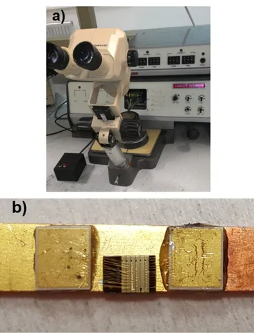
needle and align it on In paste with the pick and place instrument under optical microscope. Finally, we place the laser chip on In solder film and heat the copper plate up to the 190◦C; then we wait to cool In solder. We stick bonding pads on a copper plate by epoxy, and we have wire bonded top metal to the bonding pad by wedge bonder. The wire bonder and wire bonded lasers are shown in figure 3.7(a and b).
3.4
Characterization techniques
3.4.1
L-I-V characteristics and optical spectrum analysis
Electro-optical performance of the high-power laser diodes is extracted from the current-voltage-power measurements. We can find the threshold current (Ith),
slope efficiency (S), maximum power conversion efficiency, PCE (ηc) and series
resistance (Rs) from the current-voltage-power characteristics. We characterize
the lasers in two regimes of pulsed and continuous wave (CW) at room temper-ature.
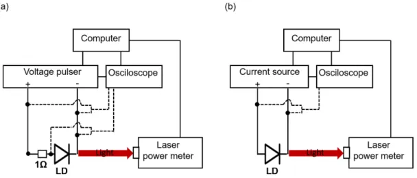
Figure 3.8: Schematics of the a) pulsed and b) CW measurement set-ups.
For pulsed measurements, we used an AVTECH voltage source. We connected a 1 resistor in series with the laser diode to measure the current. The set-up
for pulsed measurements is shown in figure 3.8a. For power measurements, we used a thermopile detector up to 2W (front facet power) with associated error of less than ±5% or an InGaAs photodedector with an integrating sphere for powers(front facet power) higher than 2W with a measurement error in the range of ±13%. The slope efficiency and threshold measurements were made in CW operation at low pump current (1A) where the power-current characteristic is linear and the measurement error is low. For CW characterization, we used ILX lightwave LDX-3600 current source. The set-up for CW measurements is shown in figure 3.8b.
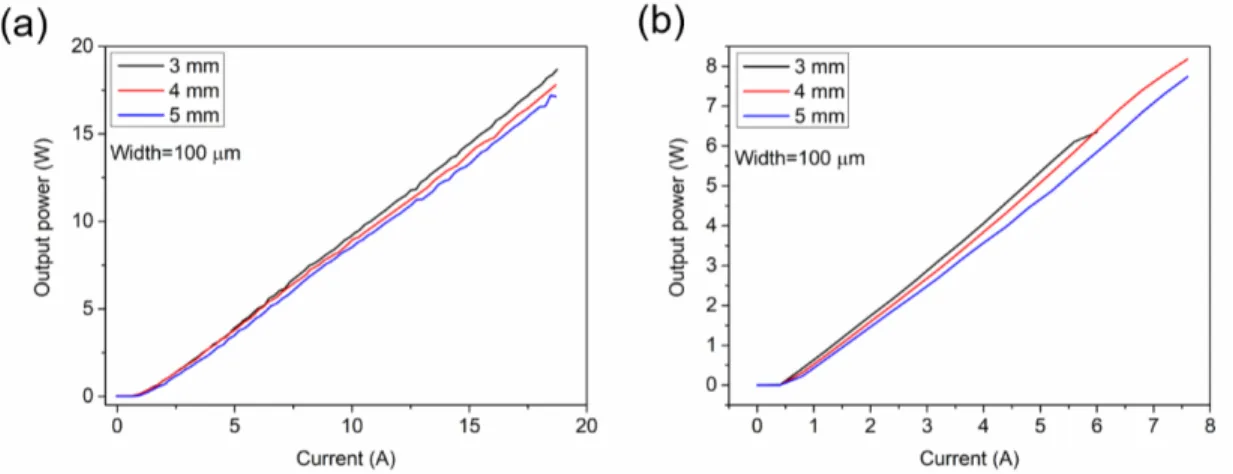
Figure 3.9: L-I measurements of 3.00, 4.00 and 5.00 mm long lasers under (a) pulsed and (b) CW operations.
We characterized 100 µm width high power broad area lasers with 3.00, 4.00 and 5.00 mm cavity lengths. In figure 3.9, the L-I characteristics of these lasers under pulsed and CW operation are given. Pulse duration was 500 ns and repe-tition rate was 2 kHz corresponding to 0.04% duty cycle. We tested lasers under short pulse regime because active region temperature increases with duty cycle and overheating leads to laser damage. In short pulse regime, we preserve the op-tical characteristics of the lasers by decreasing active region temperature. Thus, the maximum peak power is strongly increased [18]. We measured the front facet power and we found the optical output power of the uncoated lasers by multi-plying front facet power by two because the back and front facet reflectivities are equal. We achieved pulsed and CW output power greater than 18W and 8W, respectively. Laser output power becomes higher by increasing PCE [2]. The
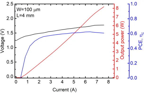
Figure 3.10: The L-V and PCE as a function of operating current for the 4.00 mm long laser under CW operation.
maximum output power and PCE obtained from epi-down mounted high-power diode lasers emitting at 9xx nm are ∼33%W and ∼65%, respectively [32, 17]. In figure 3.10, we showed the L-V and PCE as a function of operating current for 4.00 mm long laser under CW operation. Maximum PCE obtained from our lasers is ∼60%. Smaller value of output power and PCE is due to the epi-up testing. In the epi-up configuration, thermal resistance is much higher than epi-down, and it prevents the perfect cooling of the lasers [33].
In order to measure optical spectrum, the laser light is collected by a multi-mode optical fiber (0.22 NA) which is connected to the optical spectrum analyzer (Ocean Optics HR200+, spectral wavelength 190-1100 nm, resolution 0.04 nm). The emission wavelength of our lasers is around 920 nm. In figure 3.11, we show the optical spectra of the (4.00 mm)X (100 µm) laser under various CW opera-tion currents of 1.5A, 2A, and 3A and as an inset, we indicated the spectral line width and emission wavelength as a function of operating currents. The emission
Figure 3.11: The optical spectra of the 4.00 mm long broad area laser for different CW operation currents. Inset represents the spectral line width and wavelength of this laser as a function of operation current.
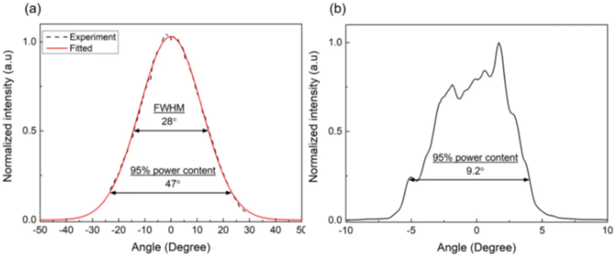
wavelength makes red-shift with increasing operation current because active re-gion temperature increases due to the Joule heating. The spectral line width of the high power broad area lasers is between the 4-5 nm at the 95% power content, and it increases with temperature [34]. The spectral linewidth of this laser under CW 1.5A, 2A, and 3A operation current is 4.00 nm, 4.17 nm, and 4.35 nm at 95% power content, respectively. Also, we showed the FWHM of the spectral line width as 2.17 nm, 2.35 nm and 2.54 nm for various current of 1.5A, 2A and 3A.
3.4.2
Internal loss and internal efficiency analysis
Internal loss (αi), internal efficiency (ηi), and transparency current density (JT r)
are obtained from the length dependence measurements. The cavity length de-pendence differential external efficiency is expressed as below
1 ηd ext = 1 ηst i + αi ηst i lnR1 L (3.1)
ηdext= dNph dN =
dP/dI ¯
hw/q (3.2)
where Nph is the number of the emitted photon through the laser facet per
unit time and N is the number of injected charged carriers per unit time.
Figure 3.12: Inverse external differential efficiency versus cavity length.
Plotting the inverse differential external efficiency as a function of cavity length and performing the linear fit, we can find the internal loss from the slope and internal efficiency from the intercept. In figure 3.12, the inverse differential effi-ciency versus cavity length graph is given for high power laser diodes with 100 µm width. These lasers were fabricated using the conventional laser process described in the fabrication section. We obtained 0.39 cm1 internal loss and 86% internal quantum efficiency from the CW measurements. These results are consistent with our theoretical expectations.
Jtrd = Jth0 − αide g0 τ Γ = J 0 th− αi(tan Θ/2ln( 1 RfRr )) (3.3)
Figure 3.13: The threshold current density as a function of inverse cavity length (Copyright 2018 IEEE [36]).
where J0
th is the threshold current density at the infinite cavity length, αi is
the internal loss, g0 is the differential gain, τ is the carrier lifetime, d is the active layer thickness, e is the electron charge, and Γ is the optical confinement factor. Plotting the threshold current density, Jth, versus inverse cavity length, 1/L, and
performing the linear fit give Jth0 from the intercept and tan θ from the slope. We know the rear and front reflectivities of Rr and Rf, therefore we can calculate
the transparency current density using the αi obtained from the cavity length
dependent inverse differential external efficiency calculated above. In figure 3.13, the threshold current density as a function of inverse cavity length is given for high power diode laser with 100 µm width. The J0
th and tan θ are found as 77±7
A/cm2 and 18±3 A/cm. αi is equal to 0.39 cm1 and uncoated facet reflectivity of
Rr and Rf are the same and equal to 0.32. We calculated transparency current
3.4.3
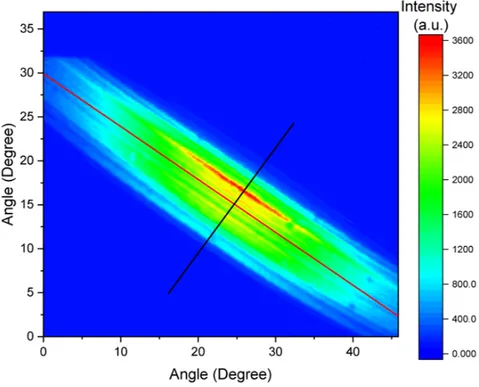
Far-field measurements
We measured the lateral and vertical far-field profiles of the 100 µm width and 4.00 mm long broad area lasers fabricated in our laboratory. We calculated the lateral and vertical FWHM divergence angle from the angled dependent intensity profiles. There are many ways to measure far-field profiles of the high-power diode lasers. One way is scanning the divergent beam with a photodiode with a slit on a motorized rotating arm (goniometer). Similarly, the divergent beam can be scanned by rotating laser diodes instead of the photodiode. The uncertainty of the divergence angle depends on the slit dimension and the distance between the laser diodes and photodiode. Another way is to use a three lens systems. Lens system also allows us to measure the near-field beam profile. The first lens in front of the laser diode is an aspheric plano-convex lens to collimate laser beam and a second plano-convex lens is a focusing lens. For near-field measurements, the photodiode with a slit is put at the focal length of the focusing lens. This lens system magnifies the image at the amount of the ratio of the focal lengths of the focusing lens and collimating lens. For far-field measurements, the third lens with a smaller focal length than that of the focusing lens is put at the place where it is one focal length of the third plano-convex lens apart from the photodiode. We can find the angle from the ratio of the beam width and focal length of the third lens. However, this is the magnified image of the far-field therefore, we have to divide by the magnification where the unit of the angle is radian.
The schematic illustration of our lateral and vertical far-field beam profile characterization set-up is given in figure 3.14. The laser light directed into the photodiode using galvo mirrors. By changing the rotation angle of the galvo mirrors, we measured the intensity using a photodiode. We put 250 µm width slit in front of the photodiode to decrease the uncertainty of the far-field divergence angle. The correction factor is required for rotation angle because of their shift between the rotation axes of the galvo mirror and the laser facet. The angle correction is given in below
![Figure 3.13: The threshold current density as a function of inverse cavity length (Copyright 2018 IEEE [36]).](https://thumb-eu.123doks.com/thumbv2/9libnet/5911494.122521/52.918.241.726.180.638/figure-threshold-current-density-function-inverse-cavity-copyright.webp)