Realization of Low-Voltage Modified CBTA and
Design of Cascadable Current-Mode All-Pass Filter
Umut Engin AYTEN
1,
Mehmet SAGBAS
2, Shahram MINAEI
31 Dept. of Electronics and Comm. Engineering, Yildiz Technical University, Esenler, 34222, Istanbul, Turkey 2 Dept. of Electric-Electronics Engineering, Yeni Yuzyil University, Zeytinburnu, 34010, Istanbul, Turkey 3 Dept. of Electronics and Communications Engineering, Dogus University, Acibadem, Kadikoy, 34722, Istanbul, Turkey
[email protected], [email protected], [email protected]
Abstract. In this paper, a low voltage modified current
backward transconductance amplifier (MCBTA) and a novel first-order current-mode (CM) all-pass filter are presented. The MCBTA can operate with ±0.9 V supply voltage and the total power consumption of MCBTA is 1.27 mW. The presented all-pass filter employs single MCBTA, a grounded resistor and a grounded capacitor. The circuit possesses low input and high output imped-ances which make it ideal for current-mode systems. The presented all-pass filter circuit can be made electronically tunable due to the bias current of the MCBTA. Non-ideal study along with simulation results are given for validation purpose. Further, an nth-order cascadable all-pass filter is also presented. It uses n MCBTAs, n grounded resistors and n grounded capacitors. The performance of the pro-posed circuits is demonstrated by using PSPICE simula-tions based on the 0.18 µm TSMC level-7 CMOS technology parameters.
Keywords
Modified current backward transconductance amplifier (MCBTA), current-mode circuits, all-pass filter, active networks.
1. Introduction
All-pass filters (APF) are widely used in analog sig-nal processing in order to shift the phase while keeping the amplitude constant, to produce various types of filter char-acteristics, and to implement high-Q frequency selective circuits. Therefore, numerous circuits are proposed in the literature for realizing all-pass filters (see [1-11] and the references cited therein). However most of these circuits suffer from the use of excessive number of active compo-nents. Since power consumption is one of the most impor-tant parameters for the circuit designers, they look for simple structures employing no more than one active ele-ment. Use of large number of passive components, lack of electronic tunability, use of floating capacitors, and unsuit
ability for cascade connection are some of the other disad-vantages which we may encounter in previously reported all-pass filters. The proposed circuits in references [1-6] operate in voltage-mode (VM). In addition, the circuit in ref. [7] operates in transadmittance-mode (TAM) where the input is voltage, the output is current. However, the CM based filters where both input and outputs are current [8-16] have been considered favorable owing to properties such as design simplicity, greater linearity, wider dynamic range, higher usable gain, and low power consumption compared with their VM counterparts.
Active circuits and other signal processing circuits play an important role in electronics. One of the versatile components for such applications is current backward transconductance amplifier (CBTA) proposed in 2010 [17]. As a consequence by using CBTA, grounded and floating inductance simulators [18], [19], frequency dependent negative resistor (FDNR) [19], and voltage- and current-mode filters [7], [17], [20-22], oscillators [23], [24], mutu-ally coupled circuit [25] and multiphase sinusoidal oscil-lator [26] are presented in the literature.
In this paper, firstly, a low-voltage low-power modi-fied CBTA (MCBTA) is proposed and discussed. Then, a new CM APF filter is proposed. The proposed APF employs one grounded capacitor, one grounded resistor and one MCBTA. It has low input current and high output impedance properties which make it ideal for cascade con-nection. The proposed CM APF is compared with some other previously reported ones as shown in Tab. 1. Al-though, the filters in [13] and [14] employ less passive component than the proposed filter, they use an active component namely; the z-copy current differencing trans-conductance amplifier (ZC-CDTA) which has more termi-nal than the MCBTA. In fact the implementation of the ZC-CDTA needs more transistors than MCBTA which consequently brings more power consumption and larger chip area. Further, a new current-mode general nth-order cascadable all-pass filter by cascading n first order all-pass section is proposed. It employs n grounded capacitors, n grounded resistors, and n active components. Finally, the simulation results are given for verifying the theoretical analysis.
* Composed of two NMOS transistors
2. Modified Current Backward
Transconductance Amplifier and
Circuit Description
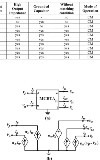
A recent publication introduced the concept and im-plementation of a circuit building block termed CBTA [17]. CBTA is proven useful in many voltage-mode and current-mode analog signal processing applications, such as current-mode and voltage-mode filters, and immittance function simulators; see for example [7], [17-26]. The MCBTA is obtained by modifying the CBTA active com-ponent that introduced in [17]. The symbol of the MCBTA and its equivalent circuit are shown in Fig. 1, where p and
n are input terminals, w, and z are output terminals. In
comparison to the CBTA, the MCBTA differs in the rela-tionship between currents Iw and Ip. While in CBTA Ip = Iw
(ideally), for the MCBTA we define Ip = -Iw. This will
simplify the internal CMOS structure of the MCBTA in comparison to CBTA. The MCBTA terminal equations can be defined as
Iz = Izc = gm(s)(Vp − Vn), Vw = µw(s)Vz,
Ip = -αp(s)Iw, In = -αn(s)Iw. (1)
The parameters αp(s), αn(s), μw(s) and gm(s) in (1) are
the current, voltage or transconductance gains between the respective terminals. They can be expressed as;
αp(s) = ωαp(1 – εαp)/(s + ωαp), αn(s) = ωαn(1 – εαn)/(s + ωαn),
μw(s)=ωµ(1 – εw)/(s + ωµ), gm(s)=goωgm(1– εgm)/(s + ωgm)
where |εαp|, |εαn|, |εgm| known as tracking errors are ideally
equal to zero, go is the DC transconductance gain. Also
ωαp, ωαn, ωgm, ωµ denote corner frequencies. Note that, in
the ideal case, the voltage and current gains (μw(s), αp(s),
αn(s)) are equal to unity.
The number of z-output terminals of the MCBTA can be increased easily by extending current mirrors used in its internal structure. In this case, the currents of the copied z terminals are defined as Izc = gm(s)(Vp − Vn). Meanwhile,
the voltage at w terminal is dependent only to the z terminal.
Fig. 1. (a) Block diagram of MCBTA. (b) Equivalent circuit of the MCBTA.
The CMOS implementation of the MCBTA is shown in Fig. 2. It consists of a transconductance stage [27] and a current conveyor stage [28]. The internal circuit of the MCBTA is simpler than CBTA since there is no need to invert the current of the p terminal. Therefore smaller number of transistors is used in the internal structure of the MCBTA than CBTA. The dimensions of the MOS tran-sistors used in the MCBTA implementation are given in Tab. 2. As seen from Fig. 2, the transistors M13–M22 are
used for realizing a dual-output transconductance stage, while transistors M2–M12 form a current conveyor. In
addition the current source IREF and transistor M1 are
employed for biasing purpose. The input voltage is defined as vin = vp − vn, and io is the output current of the
transcon-ductance stage. The output current io can be found as:
in B in m o g v I K v i ( 2 ) (2)
where K = μCoxW18,19/2L18,19, µ is the mobility of the
car-rier, Cox is the gate-oxide capacitance per unit area, W18,19
is the effective channel width, L18,19 is the effective channel
length of the transistors M18-M19 and IB is the bias current
Fig. 2. CMOS implementation of MCBTA. PMOS Transistors W(m)/L(m) M1–M5 7.2/0.36 M6, M7 3.6/0.36 M13–M17 11.52/1.44 NMOS Transistors W(m)/L(m) M8, M9 1.8/0.36 M10–M12 3.6/0.36 M18, M19 4.5/0.36 M20–M22 5.76/1.44
Tab. 2. Dimension of the CMOS transistors.
3. DC and AC Characteristics of the
MCBTA
The characteristics of the proposed circuits have been verified using PSPICE simulations. The MCBTAs are simulated using the schematic implementation shown in Fig. 2, with DC power supply voltages equal to
VDD = VSS = 0.9 V. IREF and IB are chosen as 100 A. The
simulations are performed using 0.18 m level-7 TSMC CMOS technology parameters. Some of the technology parameters used in PSPICE simulations are given as follows: threshold voltage VTH0 = 0.3725 V, low field
mo-bility U0 = 259.53 cm2/Vs, and gate oxide thickness
Tox = 4.1.10-9 m for the NMOS transistor in addition to
VTH0 = 0.3948 V, U0 = 109.976 cm2/Vs, and Tox =
4.1.10-9 m for the PMOS transistor. The power
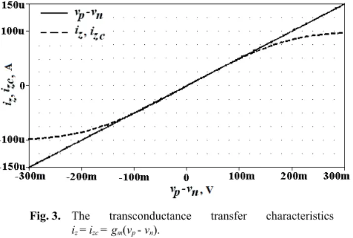
consump-tion of the MCBTA is 1.27 mW. The DC transconductance transfer characteristics of iz and izc against vp-vn when
gm = 0.5 mS are shown in Fig. 3. For this simulation, a DC
voltage sweep between −0.9 V ≤ (vp − vn) ≤ 0.9 V was
applied to the p and n terminals of the MCBTA. The output
z terminal current was measured while 1 TΩ resistor was
connected to the w output of the MCBTA and the output z terminal was grounded. It can be seen that the MCBTA works linearly between −70 µA ≤ iz ≤ 70 µA and
−140 mV ≤ vp − vn ≤ 140 mV with an error less than 1 %.
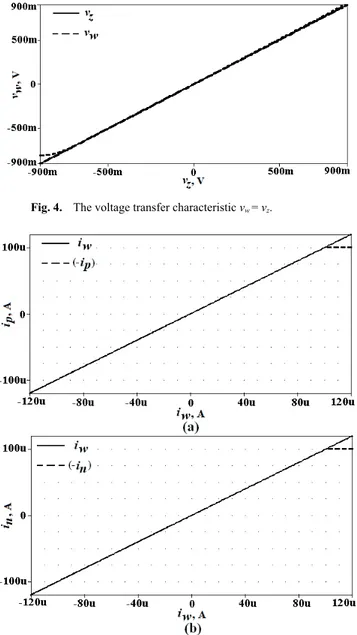
The DC characteristic of vw versus vz for the proposed
MCBTA is obtained as shown in Fig. 4. The DC voltage of
Fig. 3. The transconductance transfer characteristics iz = izc = gm(vp - vn).
the z terminal is sweep between −0.9 V ≤ vz ≤ 0.9 V and the
output voltage at w terminal was measured while the p and
n terminals were grounded. From Fig. 4 it can be seen that
the MCBTA works linearly between −0.75 V ≤ vw ≤ 0.85 V
with an error less than 1 %.
In addition, the DC current transfer characteristics of
ip and in terminal currents versus iw are extracted and
shown in Figs. 5a and 5b, respectively. The iw current was
changed between −120 µA and 120 µA and the p and n terminal currents were measured while the z, p and n ter-minals were grounded. As it can be seen from Fig. 5a and b, the MCBTA works linearly between −120 µA ≤ -ip ≤
105 µA with an error less than 1 %.
In addition, the AC analysis of the CMOS imple-mentation of the MCBTA given in Fig. 2 is investigated. The frequency characteristics, non-ideal parameters (cur-rent, voltage and transconductance tracking errors and their corner frequencies) and the maximum operating frequency of the MCBTA are found. The frequency responses of the transconductance gain |gm||Iz/(VpVn)|, the voltage gain |w||Vw/Vz|, and the current gains |p||Ip/Iw|,
| / | |
|n In Iw are given in Figs. 6 (a-c), respectively. It should be mentioned that the same simulation results are obtained for Ip/Iw and In/Iw both given in Fig. 6c.
Fig. 5. The current transfer characteristics a) ip versus iw,
b) in versus iw.
From these simulation results, corner frequencies are found as ωαp = 9610, ωαn = 9610, ωgm = 650, ωµ = 9675
Mrad/s and errors of these gains are εαp = 0.0013,
εαn = 0.0013, εgm = −0.02 and εµ = −0.079, where, go is
0.5 mS by choosing IB = 100 µA. As a result, the maximum
operating frequency of the MCBTA can be found as fol-lows fmax = min{fαp, fαn, fgm, fμ} ≈ 104 MHz.
Fig. 7 shows the non-ideal case and high frequency applications device model of the MCBTA, including es-sential non-idealities such as the high level input and out-put terminal resistances (Rp, Rn, Rz, Rzc), the low level
out-put resistance (Rw) and the input and output capacitances
(Cp, Cn; Cz, Czc). This approach is almost acceptable,
pro-vided that the implementations of the active devices do not employ multi-stage or complicated parts, which may insert additional poles or zeros to the frequency responses. The parasitic resistances and capacitances values of the MCBTA for proposed CMOS implementation are given in Tab. 3.
Fig. 6. Frequency responses; a) the transconductance gain, b) voltage gain, c) current gains.
Fig. 7. Parasitic resistance and capacitance of the MCBTA. Parasitic Impedances Values
Rp 50.1 kΩ Rn 50.1 kΩ Rz 249 kΩ Rzc 249 kΩ Rw 75 Ω Cp 180 fF Cn 180 fF Cz 244 fF Czc 196 fF
4. MCBTA Based All-Pass Filter
Design
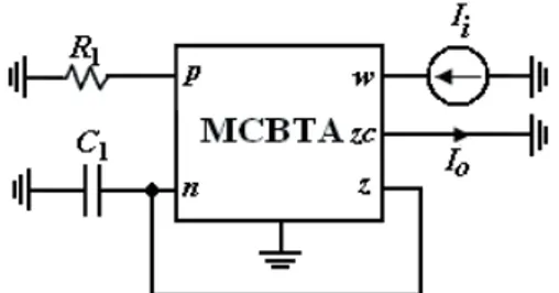
Consider an inverting first-order all-pass (AP) transfer function given by
s s s T )( . (3)
The proposed current-mode first-order AP filter is shown in Fig. 8. Nodal analysis using (1) yields the fol-lowing current transfer function
1 1 1 / / ) ( ) ( ) ( C g s C g R sg s I s I s T m m m i o . (4)
From (4), the R1 resistor should be chosen as
gm = 1/R1. Therefore, σ = gm/C1 and the ideal transfer
function T(s) has a unity gain and a frequency dependent phase given by
T(s) = 2tan-1(ωC
1/gm) for gm = 1/R1. (5)
Fortunately, this matching condition does not affect the AP filter characteristics because it is orthogonally controlled with the external resistor R1.
Fig. 8. MCBTA-based current mode first order all-pass filter.
4.1. Effect of Tracking Errors
Fig. 1b shows the equivalent circuit of MCBTA. Here
αp(s), αn(s) and μw(s) are the current and voltage gains,
respectively. gm(s) is the transconductance gain as defined
before.
The effect of the tracking errors can be found from the traditional analysis and by using non-ideal terminal equation of the MCBTA, the current transfer function of the circuit can be written as
1 1 1 ) ( ) ( C g s C g R g s s I s I m m n m p i o . (6)
Comparing (6) and (4) it can be realized that the pole of the proposed all-pass filter transfer function does not affect from the non-ideality parameters of the MCBTA.
4.2. Effect of Terminal Impedances
Considering the parasitic resistances (Rp, Rn; Rz, Rzc,
Rw) and capacitances (Cn, Cp; Cz, Czc) shown in Fig. 7, the
total impedances at nodes terminals p and n for the circuit of Fig. 8 can be given as follows
ZR1 = R1||Rp||(1/sCp), (7a)
ZC1 = Rn||Rz||(1/sC1)||(1/sCn)||(1/sCz). (7b)
Therefore, the non-ideal the transfer function of the circuit in terms of αp, αn, ZR1 and ZC1 can be given as,
1 ( ) ( 1 1 1 C m C n R p m Z g Z Z g s T . (8)
The non-ideal input and output impedances of the proposed filter can be found as follows
Zi = Rw, Zo = Rzc||(1/sCzc). (9)
In ideal condition the output has infinitive impedance property since Rzc is the high impedance output terminal of
the MCBTA and Czc is almost zero (see Tab. 3). Moreover,
since Rw of the MCBTA has low value (ideally zero) the
proposed circuit enjoys low input impedance property. Therefore the proposed all-pass filter is fully cascadable. Further, the parasitic impedances can be compensated by choosing the external resistor value (R1) small enough with
respect to the terminal resistance (Rp) and the external
capacitor value large enough with respect to the terminal capacitances (Cz, Cn).
5. Design of nth-order All-Pass Filter
The general all-pass filters have the transfer function
) ( ) ( ) ( ) ( ) ( s D s D s I s I s T i o . (10)
Equation (10) can be rewritten the multiplication of the n all-pass sections as follows
n i i i s s s s s T 1 ) ( , Re {si}>0, i=1,2,…, n (11)where T(s) is the all-pass function defined by the open right half of s-plane poles si. If all of the poles/zeros of T(s)
are real, it can be realized by cascading n first-order all-pass filter of Fig. 8 with transfer function given in (4). The result is shown in Fig. 9. In this case the transfer function on the obtained nth order all-pass filter is given as
n i mi i i mi i mi C g s C g R sg s T 1 ) / / ( ) ( (12) where gmi = 1/Ri and si = gmi/Ci, I = 1, 2, …, n.Results
The fourth-order all-pass filter circuit is realized to verify the performance of the proposed nth-order all-pass filter circuit as an example. The proposed fourth-order all-pass filter transfer function is determined to be
1 1 1 1 37 . 1 37 . 1 73 . 0 73 . 0 1 2 1 2 1 1 . 2 1 1 . 2 ) ( ) ( ) ( 1 2 22 22 s s s s s s s s s s s s s s s s s T s T s T . (13)
The passive components values of the 4th-order
all-pass filter can be found as follows; Section I: C1 = 1/(0.73R1ωc), gm1 = 1/R1
Section II: C2 = 1/(1.37R2ωc), gm2 = 1/R2
Section III: C3 = 1/(R3ωc), gm3 = 1/R3
Section IV: C4 = 1/(R4ωc, ) gm4 = 1/R4.
The angular frequency is scaled by ωc = 2π×106 rad/s.
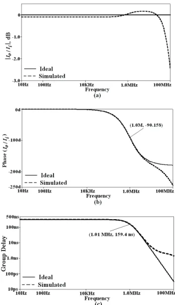
Firstly, the simulation is done for the first-order all-pass filter circuit shown in Fig. 8. gm and R1 are chosen as
0.5 mS and 2 kΩ, respectively and C1 is found 79.58 pF for
fc = 1 MHz. The gain, phase and group delay characteristics
of the proposed first-order all-pass filter can be seen in Fig. 10.
To test the input dynamic range of the proposed cur-rent-mode first-order all-pass filter, the time-domain simu-lation of the all-pass filter as an example has been per-formed for a sinusoidal input signal at f = 1 MHz. Fig. 11 shows the time-domain response of the filter where an amplitude of 140 μA (peak to peak) is obtained at the output without significant distortion. The THD value for the current output is less than 0.1% and the total power dissipation of the proposed all-pass filter is found to be 1.27 mW. The famous X–Y pattern (Lissajous pattern) for the circuit as -90o phase shifter is shown in Fig. 13. Since
the amplitudes of the input and output of the proposed APF are different, the shape of the simulated phase characteris-tic in Fig. 12 looks like ellipsis.
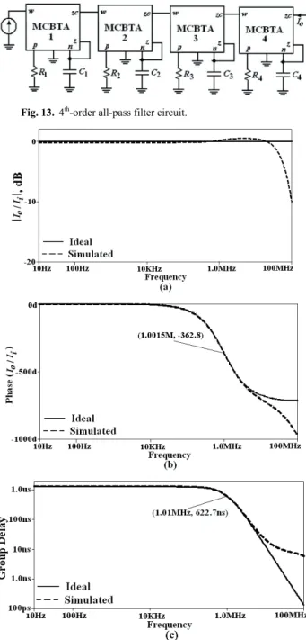
The 4th-order all-pass filter circuit using the MCBTA
is shown in Fig. 13. This circuit is obtained by cascading four all-pass filter circuits shown in Fig. 8.
Fig. 10. a) Gain, b) Phase, c) Group delay characteristics of the proposed first-order all-pass filter.
Fig. 11. The input and output waveforms of the proposed first-order all-pass filter.
The proposed 4th-order all-pass filter circuit is built
with R1 = R2 = R3 = R4 = 1/gm = 2 kΩ, gm = 0.5 mS, and
C1 = 109 pF, C2 = 58 pF, C3 = C4 = 79.6 pF for fc = 1 MHz.
The simulation results with respect to ideal ones are shown in Fig. 14. It can be seen that the simulated and theoretical
magnitude and phase responses of the all-pass filter are in good agreement
Fig. 12. Lissajous pattern (Io against Iin) for the proposed AP
filter.
Fig. 13. 4th-order all-pass filter circuit.
Fig. 14. a) Gain, b) Phase, c) Group delay characteristics of the proposed 4th-order all-pass filter circuit.
From simulation, the gain values of the proposed cir-cuit are 0.98 for frequencies lower than 500 kHz and 1.0152 for the corner frequency 1 MHz, while the theoreti-cal value is one. The phases are measured to be -0.7o at low
frequencies and -362o at 1 MHz while they are 0o and 360o
respectively for ideal case.
A sinusoidal input current with 70 μA peak value is applied to the circuit and the output signal is observed as shown in Fig. 15a. The simulation results are found in very good agreement with the ideal ones. The FFT spectrum of the input and output signals are shown in Fig. 15b. The THD value for the current output is 2.52% and the total power dissipation of the proposed 4th-order all-pass filter
circuit is found to be 5.08 mW.
Fig. 15. a) The input and output waveforms of the proposed 4th
-order all-pass filter circuit, b) FFT spectrum of the current output.
7. Conclusion
A novel low-voltage low-power MCBTA is proposed and verified through PSPICE simulation using 0.18 µm TSMC level-7 CMOS technology parameters. The MCBTA operates at a low supply voltage of only ±0.9 V and a total power consumption of only 1.27 mW. A novel first-order current-mode all-pass filter using two grounded passive component and one MCBTA is also proposed. The proposed circuit has the advantage of having low input and high output impedances which makes it for easy cascad-ability. Further, a nth-order all-pass filter topology which
and Applications, 2008, vol. 36, p. 511–512.
[2] CHANG, C. M., SOLIMAN, A. M., SWAMY, M. N. S. Analytical synthesis of low sensitivity high-order voltage-mode DDCC and FDCCII-grounded R and C all-pass filter structures. IEEE Transactions Circuits and Systems I-Regular Papers, 2007, vol. 54, p. 1430–1443.
[3] BIOLEK, D., BIOLKOVA, V. All-pass filters employing differential op amps. Electronics World, 2010, vol. 116, no. 1891, p. 44 – 45.
[4] METIN, B., PAL, K. Cascadable allpass filter with a single DO-CCII and a grounded capacitor. Analog Integrated Circuits and Signal Processing, 2009, vol. 61, no. 3, p. 259–263.
[5] HERENCSAR, N., KOTON, J., JERABEK, J., VRBA, K., CICEKOGLU, O. Voltage-mode all-pass filters using universal voltage conveyor and MOSFET-based electronic resistors. Radioengineering, 2011, vol. 20, no. 1, p. 10–18.
[6] MINAEI, S., YUCE, E. Novel voltage-mode all-pass filter based on using DVCCs. Circuits, Systems, and Signal Processing, 2010, vol. 29, p. 391–402.
[7] HERENCSAR, N., LAHIRI, A., KOTON, J., SAGBAS, M., AYTEN, U. E. VRBA, K. New MOS-C realization of transadmittance type all-pass filter using modified CBTA. In Proceeding of International Conference on Applied Electronics (AE 2011). Pilsen (Czech Republic), 2011, p. 153 - 156.
[8] MINAEI, S., CICEKOGLU, O. New current-mode integrator and all-pass section without external passive elements and their applications to design a dual-mode quadrature oscillator. Frequenz, 2003, vol. 57, no. 1-2, p. 19-24.
[9] YUCE, E., MINAEI, S., HERENCSAR, N., KOTON, J. Realization of first-order current-mode filters with low number of MOS transistors. Journal of Circuits, Systems, and Computers, 2013, vol. 22, no. 1, 1250071 14 p.
[10] TANGSRIRAT W., PUKKALANUN, T., SURAKAMPON-TORN, W. Resistorless realization of current-mode first-order allpass filter using current differencing transconductance amplifiers. Microelectronics Journal, 2010, vol. 41, p. 178–183. [11] JAIKLA, W., NOPPAKARN, A., LAWANWISUT, S. New gain
controllable resistor-less current-mode first order allpass filter and its application. Radioengineering, 2012, vol. 21, no. 1, p. 312-316. [12] MAHESHWARI, S. High output impedance current-mode all-pass
sections with two grounded passive components. IET Circuits Devices and Systems, 2008, vol. 2, no. 2, p. 234–242.
[13] LAHIRI, A., CHOWDHURY, A. A novel first-order current-mode all-pass filter using CDTA. Radioengineering, 2009, vol. 18, no. 3, p. 300-305.
[14] PANDEY, N., PAUL, S. K. Single CDTA-based current mode all-pass filter and its applications. Journal of Electrical and Computer Engineering, 2011, vol. 2011, Article ID 897631.
of Electronics and Communications, 2011, vol. 65, p. 794-798. [19] AYTEN, U. E., SAGBAS, M., HERENCSAR, N., KOTON, J.
Novel floating general element simulators using CBTA. Radioengineering, 2012, vol. 21, no. 1, p. 11-19.
[20] SAGBAS, M., AYTEN, U. E., SEDEF, H. Current and voltage transfer function filters using a single active device. IET Circuits Devices and Systems, 2010, vol. 4, no. 1, p. 78-86.
[21] KOKSAL, M. Realization of a general all-pole current ratio transfer function by using CBTA. International Journal of Circuit Theory and Applications, 2013, vol. 41, no. 3, p. 319-329. [22] SAGBAS, M., KOKSAL, M. Realization of a general resistorless
active biquad by using CBTA. Journal of Circuits, Systems and Computers, 2012, vol. 21, no. 1, 1250013p.
[23] HERENCSAR, N., KOTON, J., VRBA, K., LAHIRI, A., AYTEN, U. E., SAGBAS, M. A new compact CMOS realization of sinusoidal oscillator using a single modified CBTA. In Proceeding of 21st International Conference Radioelektronika. Brno (Czech Republic), 2011, p. 41 - 44.
[24] AYTEN, U. E., SAGBAS; M., SEDEF, H. Electronically tunable sinusoidal oscillator circuit with current and voltage outputs. Int. Journal of Electronics, 2012, vol. 99, no. 8, p. 1133-1144. [25] KOKSAL, M., AYTEN, U. E., SAGBAS, M. Realization of new
mutually coupled circuit using CC-CBTAs. Circuits, Systems, and Signal Processing, 2012, vol. 31, no. 2, p. 435 - 446.
[26] SAGBAS, M. AYTEN, U. E., HERENCSAR, N., MINAEI S. Voltage-mode multiphase sinusoidal oscillators using CBTAs. In Proceedings of the 2012 35th International Conference on Telecommunications and Signal Processing (TSP 2012). Prague (Czech Republic), 2012, p. 421 - 425.
[27] KAEWDANG, K., SURAKAMPONTORN, W. On the realization of electronically current-tunable CMOS OTA. AEU-International Journal of Electronics and Communications, 2007, vol. 61, p. 300 to 306.
[28] GUNES, E. O., ZEKI, A., TOKER, A. Design of a high performance mutually coupled circuit. Analog Integrated Circuits and Signal Processing, 2011, vol. 66, no. 1, p. 81-91.
About Authors ...
Umut Engin AYTEN received the M.Sc. and Ph.D.
de-grees in Electronics Engineering from the Yildiz Technical University, Istanbul, Turkey, in 2003 and 2009, respec-tively. He is currently an Asst. Professor at Yildiz Techni-cal University. His current field of research concerns ana-log integrated circuits, active filters, current-mode circuits and analog signal processing.
Mehmet SAGBAS received his B.S. degree in Electronics
Engineering from the Istanbul Technical University in 2000. He received his M.S. degree in Electronics Engi-neering from the Fatih University in 2004. He received his Ph.D. degree in Electronics Engineering from the Yildiz Technical University in 2007. He is currently an Assoc. Professor at Yeni Yuzyıl University. His research interests are analog integrated circuits and analog signal processing.
Shahram MINAEI received the B.Sc. degree in Electrical
and Electronics Engineering from Iran University of Sci-ence and Technology, Tehran, Iran, in 1993 and the M.Sc.
and Ph.D. degrees in Electronics and Communication En-gineering from the Istanbul Technical University, Istanbul, Turkey, in 1997 and 2001, respectively. He is currently a Professor in the Department of Electronics and Commu-nication Engineering, Dogus University, Istanbul, Turkey. He has more than 140 publications in scientific journals or conference proceedings. His current field of research con-cerns current-mode circuits and analog signal processing. Dr. Minaei is a senior member of the IEEE, an associate editor of the Journal of Circuits, Systems and Computers (JCSC), and an area editor of the International Journal of Electronics and Communications (AEÜ).