WA1
8:30 am -8:45 am
Electrically-reconfigurable integrated photonic switches
Onnr Fidaner, Hilmi Volkan Demir*, Vijit A. Sabnis,James S. Harris, Jr., and David A. B. Miller
E.L. Ginzton LaboratOlY and Solid State and Photonics LaboratOlY, Stanford University, Stanford, CA 94305, USA Tel. (650) 725-2291, [email protected]
* Currently with Bilkent Nanotechnology Research Center, Bilkent University, Bilkent, Ankara TR-06800, Turkey
Jun-Fei Zheng
Strategic Technology, Intel Corporation, MIS SCI-03, 3065 Bowers Avenue, Santa Clara, CA 95052, USA
Abstract: We report remotely electrically reconfigurable photonic switches that intimately integrate waveguide electroabsorption modulators with surface-normal photodiodes, avoiding conventional electronics, These switches exhibit full C-band wavelength conversion at 5 Gb/s and are remotely reconfigurable within tens of nanoseconds, The rapid growth in Internet traffic will be sustained through the optimal use of the limited network resources, This requires increased functionality at each node in an optical network while also minimizing the cost, size and power dissipation of individual elements at each network node, Current optical networks are, however, limited in many ways by electronics, Today's optical-electronic-optical conversion (o-e-o) technology requires propagating high speed signals in the electronic domain and cascading separately packaged electronic and optoelectronic devices, which deteriorates the overall conversion efficiency [I], For o-e-o conversion without the use of conventional electronics, we introduce a chip-scale photonic switching platform to integrate waveguide electroabsorption modulators (EAM) and surface-normal photodiodes (PD) intimately on the same substrate [2], Not only does such an integrated optical switch architecture avoid the difficulties and the limitations of ordinary o-e-o conversion, but also provides multiple network functions including full C-band, arbitrary wavelength conversion during optical switching, Furthermore, these switches can be rapidly electrically enabled and disabled, allowing for fast, remote electrical reconfiguration of the network for the optimal use of its limited resources through traffic pattern engmeenng as necessary,
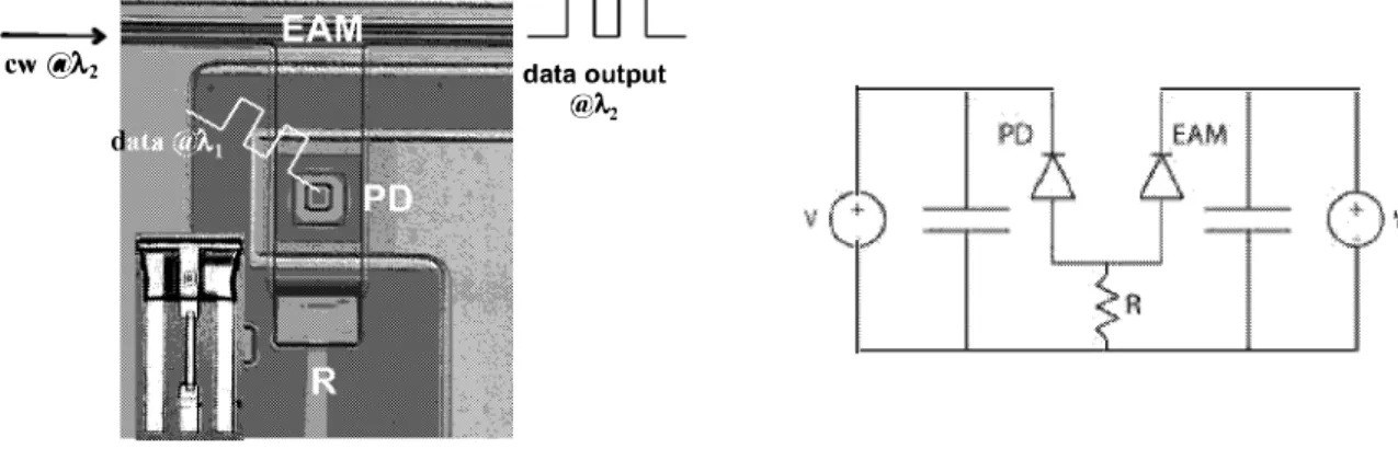
The on-chip, close integration of an InGaAs PD and an InGaAsP multiple quantum well (MQW) EAM, as shown in Fig, 1, localizes the optically-induced high-speed electrical signals within the compact integrated switch, allowing for its efficient operation with low power at high speeds, Also, since only DC biasing is required externally and high-speed signals do not have to leave the device, no high-speed electronic packaging or impedance matching is needed, which reduces the cost significantly, The PD and the EAM are tightly integrated using a selective area regrowth technique [3], With such an intimate integration, the overall chip size is confined to an area of 300 11m by 300 11m, allowing for lumped circuit operation of its integrated parts, That way, its 3 dB switching bandwidth is predominantly determined only by the internal device RC time constant The DC bias is applied through a set of external bypass capacitors to confine the high-speed signals in the switch and prevent loading from the DC biasing circuit
CW (jif).2 data output
@�
\+
VFig. 1. Plan view of a fabricated device Fig. 2. Simplified circuit diagram of the device
The InGaAsP MQW EAM exhibits strong electroabsorption in the C-band. The InGaAs PD, on the other hand, absorbs over a wide wavelength range, including the C-band. There are two optical inputs of the switch. The first
one is the surface-normal control input incident onto the PD, at wavelength ?I and the other is a continuous wave (cw) input at wavelength ?2 coupled into the waveguide EAM. The DC bias applied to the EAM is set such that the MQW structure absorbs the cw input with no optical power on the PD. When an optical data is present on the control input (i.e., data at AI), the PD generates a photocurrent that causes an almost instantaneous voltage drop across the on-chip pull-up resistor (R). This voltage drop appears across the EAM, changing its absorption and allowing for transmission of the cw input. This way, the optical information is bit-by-bit transferred from the input optical data stream at Al onto the cw optical beam at 1.2.
This photonic switch architecture also allows for making two-dimensional arrays of these switches on a single chip to implement crossbar switches [4]. The ability of electrically reconfiguring such optical switch arrays is, however, critical for future network architectures that employ central network management systems. For that, the network nodes have to be configured rapidly and remotely. In our switch architecture, when the PD bias is removed, the switch is disabled. When the photocurrent extraction from the PD is suppressed, it can no longer drive the EAM. We used a 2.5 MHz -8 to I V square wave with a fallirise time of IS ns to reverse bias the PD while a cw beam was incident on it. When the signal changes from high to low, forward biasing the PD, the EAM output fades away within 40 ns. The reconfiguration time depends on the discharge time of the PD capacitance over R and hence it is theoretically expected to be on the order of a nanosecond. In our experimental setup, the use of large external bypass capacitors (45 0 pF) inhibits the ability of even faster reconfiguration. This, however, can be significantly improved by using on-chip bypass capacitors of tens of pF that are integrated to the circuit.
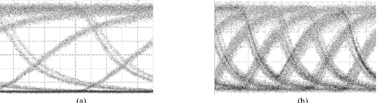
Such PD-EAM switches are capable of converting any wavelength within the C-band to any other wavelength within the C-band [2]. Fig. 3 illustrates open eye diagrams of the EAM output at 1548.5 nm when a (a) 3.5 Gb/s and a (b) 5 Gb/s no-return-to-zero (NRZ) input data stream at 155 1.7 nm is incident on the PD, as an exemplary wavelength conversion in the C-band at two different speeds.
(� �)
Fig. 3. (a) Eye diagram at 3.5 Gb/s with 1 1.7 dB RF extinction ratio (b) Eye diagram at 5 Gb/s with 5.9 dB RF extinction ratio.
In conclusion, we report remotely electrically reconfigurable, wavelength-converting photonic switches that offer a remedy for the difficulties associated with the conventional o-e-o conversion, including packaging costs and the necessity for large installation space. Based on our experimental results at 5 Gb/s and the validation of our device model, we anticipate that our switch can be further scaled to 10 Gb/s operation by appropriately reducing the on-chip resistor, progressive scaling of the device capacitances, and minimizing the parasitics.
References
[1] S. J. B. Yoo, "Wavelength conversion technologies for WDM network applications," IEEE 1. Light. Tech., 1 4 (6), pp. 955-966, ( 1 996). [2] H. V. Demir, V. A. Sabnis, O. Fidaner, J. S. Harris, Jr., D. A. B. Miller, and J.-F. Zheng, "Dual-diode quantum-well modulator for
C-band wavelength conversion and broadcasting," OSA Optics Express, 12(2), pp. 31 0-316, (2004).
[3] V. A. Sabnis, H. V. Demir, O. Fidaner, J. S. Harris, Jr., D. A. B. Miller, I-F. Zheng, N. Li, T.-C. Wu, and Y.-M. Houng, "Optically-switched dual-diode e1ectroabsorption modulators," OSA Conference on Integrated Photonics Research (IPR) , pp. 1 2- 1 4, (OSA Technical Digest, Optical Society of America, Washington, DC, 2003). Paper 1MB3.
[4] H. V. Demir, V. A. Sabnis, O. Fidaner, 1. S. Harris, Jr., D. A. B. Miller, I-F. Zheng, N. Li, T.-C. Wu, and Y.-M. Houng, "Novel scalable wavelength-converting crossbar," Proceedings of IEEE-OS A Optical Fiber Communications Conference (OFC) , Los Angeles, CA (February 22-27, 2004). Paper FD5.