i
FORMATION OF Ge NANOCRYSTALS
WITH CW LASER IRRADIATION OF
SiO
x:Ge THIN FILMS
A THESIS SUBMITTED TO
THE GRADUATE SCHOOL OF ENGINEERING AND SCIENCE OF BILKENT UNIVERSITY
IN PARTIAL FULLFILMENT OF THE REQUIREMENTS FOR THE DEGREE OF MASTER OF SCIENCE IN PHYSICS By Melike Gümüş January, 2015
ii
FORMATION OF Ge NANOCRYSTALS WITH CW LASER IRRADIATION OF SiOx:Ge THIN FILMS
By Melike Gümüş January, 2015
We certify that we have read this thesis and that in our opinion it is fully adequate, in scope and in quality, as a thesis for the degree of Master of Science.
____________________________________ Prof. Dr. Atilla Aydınlı (Advisor)
____________________________________ Prof. Dr. Oğuz Gülseren
____________________________________ Assoc. Prof. Dr. Alpan Bek
Approved for the Graduate School of Engineering and Science:
____________________________ Prof. Dr. Levent Onural Director of the Graduate School
iii
ABSTRACT
FORMATION OF Ge NANOCRYSTALS WITH CW LASER
IRRADIATION OF SiO
x:Ge THIN FILMS
Melike Gümüş M.S. in Physics
Advisor: Prof. Dr. Atilla Aydınlı January, 2015
Germanium and silicon are the materials which have effective absorption in the visible and near infrared region of electromagnetic spectrum; therefore they are preferred for optoelectronic device and solar cell applications. Si and Ge are the material of choice when it comes to solar cell applications due to their being low cost, widely available and inert. They have indirect bandgap and the absorption coefficient of indirect bandgap materials is lower than direct ones. It is known that decreasing dimensions of materials to nanometric sizes cause transition from indirect bandgap to direct bandgap behavior along with increasing band gap. Therefore decreasing their dimensions both a shift of the band gap toward the blue as well as an increase in absorption can be achieved. In this work, thin films of SiOx:Ge were
fabricated with different germanium concentrations and annealed with CW Ar+ laser operating at 488 nm that resulted in formation of Ge nanocrystals in the SiOx matrix.
Composition analysis of as grown samples were done by Rutherford Backscattering Spectroscopy, optical properties were determined by ellipsometry. Nanocrystal formation within laser irradiated samples was confirmed by Raman spectroscopy. Data were also collected about crystal formation by scanning surface texture with stylus surface profilometer. As a result of all the analysis, it was shown that crystal formation depends on germanium concentration in the SiOx matrix and laser irradiation power density.
iv
ÖZET
SiO
x:Ge İNCE FİLMLERDE SÜREKLİ DALGA LAZERİ
IŞINLAMASI İLE GERMANYUM NANOKRİSTAL
OLUŞUMU
Melike Gümüş Fizik, Yüksek Lisans
Tez Danışmanı: Prof. Dr. Atilla Aydınlı Ocak, 2015
Germanyum ve silisyum elektromanyetik spektrumun görünür ve yakın kızılötesi bölgesinde etkili soğuruculuğa sahip malzemelerdir bu nedenle optoelektronik aygıt ve güneş pili uygulamalarında tercih edilirler. Düşük maliyet, yaygun kullanım ve kararlı yapısından dolayı güneş pili uygulamalarında Si ve Ge materyalleri tercih edilmektedir. İndirekt bant aralığına sahiptirler ve indirekt bant aralıklı malzemelerin soğurma verimlilikleri direkt olanlardan daha azdır. Nanometric boyutlara azalan malzemelerin, indirekt bant aralığından, direkt bant aralığına, bant aralığı artacak şekilde geçişi sağladıkları bilinmektedir. Bu nedenle malzeme boyutlarının düşürülmesi ile, hem bant aralağında maviye doğru kaymasına hem de emilim özelliğindeki artışa ulaşılabilir. Bu çalışmada, SiOx:Ge ince filmleri farklı
germanyum konsantrasyonlarında üretilmiş ve 488 nm’de Ar+
sürekli dalga lazeri ile tavlanması, SiOx matriksinin içerisinde Ge nanokristal oluşumu ile sonuçlanmıştır. Örneklerin kompozisyon analizi Rutherford Geri Saçılma Spektroskopisi, optik özelliklerinin belirlenmesi elipsometri ile yapılmıştır. Tavlanmış örneklerdeki kristal oluşumu Raman spektroskopisi ile doğrulanmıştır. Yüzey yapısı, iğneli yüzey profilometresi ile taranarak kristal yapılanması hakkında ayrıca bilgi toplanmıştır. Tüm analizlerin sonucunda, nanokristal oluşumunun SiOx matrisinin içindeki
germanyum konsantrasyonuna ve tavlama güç yoğunluklarına bağlı olduğu gösterilmiştir.
Anahtar sözcükler: Ge nanokristaller, PECVD, ince filmler, sürekli dalgalı lazerle
v
Acknowledgement
I could not have completed my thesis without the support and guidelines of many valuable people.
I would like to present my deepest gratefulness my academic advisor Prof. Dr. Atilla Aydınlı who guided me during my thesis period with a great wisdom and patience. He helped to develop my scientific mind and kept me awake.
I would also present my gratitude to Prof. Dr. Oğuz Gülseren and Assoc. Prof. Alpan Bek for their valuable criticism as the members of my thesis committee.
I would like to thank Dr. Emel Sungur Özen for her mentorship and invaluable contributions to my thesis.
I would like to thank Salvatore Mirabella who provided the RBS data on our samples. .
I would like to thank my parents for endless support, love and encouragement and my sister for enduring communicate sessions.
I would like to thank my ‘’ fellow sufferer ‘’ (Seval Sarıtaş) for valuable friendship and our cheerful times.
I would like to thank my ‘’logical side’’ (Abdullah Muti) for his advises.
I would like to thank my officemates Ertuğrul Karademir for mentorship at all stages of my M.S. study, Simge Ateş for excellent friendship, Sinan Gündoğdu for his helps and Abdullah Kahraman.
And finally I would like to present my greatest gratitude to ‘’my lottery’’ Önder Akçaalan for bringing me back to life.
vi
Contents
1 INTRODUCTION ... 1
1.1. First Generation Solar Cells ... 3
1.2. Second Generation Solar Cells (Thin Film Solar Cells) ... 4
1.3. Third Generation Solar Cells ... 5
2 EXPERIMENTAL ... 14 2.1 Sample Preparation ... 14 2.2 Laser Processing... 16 2.3 Measurement Techniques... 20 2.3.1 Absorption Spectroscopy ... 20 2.3.2 Raman Spectroscopy ... 23 2.3.3 Ellipsometric Analysis ... 28
2.3.4 Rutherford Backscattering Technique... 31
2.3.5 Surface Profile Analysis ... 33
3 RESULTS ... 35
3.1 Characterization of As-Grown Samples... 35
3.1.1 Composition Analysis ... 35
3.1.2 Absorption Spectroscopy Analysis ... 39
3.1.3 Refractive Index Measurements ... 41
3.2 Characterization of Processed Samples ... 48
3.2.1 Crystallization of Ge in SiOx matrix ... 48
3.2.2 Surface Topography ... 52
3.2.3 Vibrational Modes and Bonding ... 56
vii
List of Figures
Figure 1. 1: Schematic of solar cell ... 2
Figure 1. 2: Schematic of loss mechanism in single junction solar cell [4, 11]: (1) non- absorption of the photons which have energies less than below the band gap; (2) energy loss due to thermalization; (3) junction loss; (4) contact voltage loss; (5) recombination loss ... 6
Figure 1. 3: Schematics of single photon creation of multiple electron-hole pair in a) bulk an in b) nanocrystals [14]. ... 7
Figure 1. 4: Schematic of multiband cells [14] ... 8
Figure 1. 5: Schematic of up / down conversion ... 8
Figure 1. 6: Schematic of III-V solar cell ... 9
Figure 1. 7: Schematic of CIGS and CdTe/CdS structures (courtesy of R. Turan) ... 10
Figure 1. 8: An example of a-Si/µc –Si-H silicon cells (courtesy of R. Turan) ... 10
Figure 1. 9: Optical gap as a function of nanocrystal diameter [22] (courtesy of C. Bulutay). ... 11
Figure 2. 1: Schematics of the PECVD reactor... 16
Figure 2. 2: Schematic of laser processing setup ... 18
Figure 2. 3: An optical microscopy image of laser processed lines with increasing powers. ... 19
Figure 2. 4: Schematic of a Fourier Transform Infrared Spectroscopy setup ... 21
Figure 2. 5: Interferogram of two monochromatic sources... 22
Figure 2. 6: Interferogram of five monochromatic sources. ... 22
Figure 2. 7: A sample for reflectance spectrum of SiOx:Ge sample ... 23
Figure 2. 8: Schematic diagram of Raman experiment ... 27
Figure 2. 9: A typical Raman Spectrum of annealed SiOx:Ge sample... 28
Figure 2. 10: Schematic diagram of ellipsometry ... 29
Figure 2. 11: A typical ellipsometry data. ... 30
Figure 2. 12: Schematics of Rutherford Backscattering experiment ... 32
Figure 2. 13: A typical RBS data for SiGeN samples. ... 33
Figure 3. 1: RBS spectrum of as-grown SiOx:Ge samples ... 36
Figure 3. 2: Simulations and experimental RBS data for samples A, B and C, respectively. ... 37
Fig. 3. 3: RBS concentrations of Ge, Si and O for different GeH4 flow rates. ... 39
viii
Figure 3. 5: Comparative reflectance measurements of, as-grown quartz for samples
A (60 sccm GeH4), B (90 sccm GeH4), and C (120 sccm GeH4) ... 41
Figure 3. 6: Raw ellipsometric data for three SiOx:Ge samples ... 43
Figure 3. 7: Fitting models of ellipsometric data of SiOx:Ge samples. ... 44
Figure 3. 8: Ellipsometric raw data with Cauchy model fit. ... 45
Figure 3. 9: Refractive indices of three SiOx:Ge samples for A (60 sccm GeH4), B (90 sccm GeH4), and C (120 sccm GeH4). ... 46
Figure 3. 10: Absorption and extinction coefficients of SiOx:Ge samples for A (60 sccm GeH4), B (90 sccm GeH4), and C (120 sccm GeH4). ... 47
Figure 3. 11: Raman Ge crystal peaks of annealed A series by various powers (linear scale). ... 49
Figure 3. 12: Raman Ge crystal peaks of laser irradiated B series by various power densities (linear scale). ... 50
Figure 3. 13: Raman Ge crystal peaks of laser irradiated C series by various power densities (linear scale). ... 51
Figure 3. 14: Threshold power densities for crystallization of A (60 sccm GeH4), B (90 sccm GeH4), and C (120 sccm GeH4) (linear scale). ... 52
Figure 3. 15: Surface profile analysis for A series by various annealing powers. ... 53
Figure 3. 16: Surface profile analysis for B series with various laser power densities. ... 54
Figure 3. 17: Surface profile analysis for C series by various laser power densities. 55 Figure 3. 18: Reflectance measurements of laser processed A (60 sccm. GeH4) series (linear scale). ... 57
Figure 3. 19: Reflectance measurements of laser processed B (90 sccm GeH4) series (linear scale). ... 58
Figure 3. 20: Reflectance measurements of laser processed C (120 sccm. GeH4) series (linear scale). ... 59
Figure 3. 21: Comparative reflectance measurements of laser processed A (60 sccm. GeH4), B (90 sccm GeH4), C (120 sccm GeH4) series (linear scale). ... 60
ix
List of Tables
Table 2. 1: List of samples prepared by PECVD ... 15 Table 2. 2: Annealing power densities per unit cm2 ... 17 Table 2. 3: Nanocrystal formation power density threshold for laser scanned samples
... 20 Table 3. 1: Si, Ge, O, N and H doses and thickness results with respect to simulation
1
Chapter 1
Introduction
The rapidly developing technology creates many opportunities to convert solar energy type electricity. In last few decades, sun has become widely preferable to other energy sources such as nuclear, fossil and hydraulics. The use of sun as an energy source has many advantages like low cost, efficiency and sustainability. Devices that convert sun into others forms of energy are convenient in various parts of life such as various industries, in space, in new generation vehicles. However, they are not yet cheap enough in comparison with non renewable energy sources.
The amount of light reaching earth every day from the sun is over 1.5 x 10²² J (15000 EJ). To collect a significant amount of this energy and convert to electricity, solar cell modules with high efficiency are needed. Many types of materials have been used to design and fabricate solar cells. Despite many efforts to increase efficiency and cost of solar modules, further research is still needed [1]. These modules are an order of magnitude higher in cost when compared with commercial nuclear, fossil and hydraulic power energy converters. Reasons of this cost are lack of cheap substrates, cost of connections and encapsulation as well as installation of solar cell modules [2]. Solar cells (also called photovoltaic devices) are environmentally friendly energy sources. They convert solar energy into electrical energy through light absorption, creation of electron-hole pairs followed by separation of charge carriers of opposite types and finally extraction of charge carriers into the circuit. Incident electromagnetic energy converts into electrical energy in a semiconductor. This process occurs as follows; photons incident onto the module penetrate into the
2
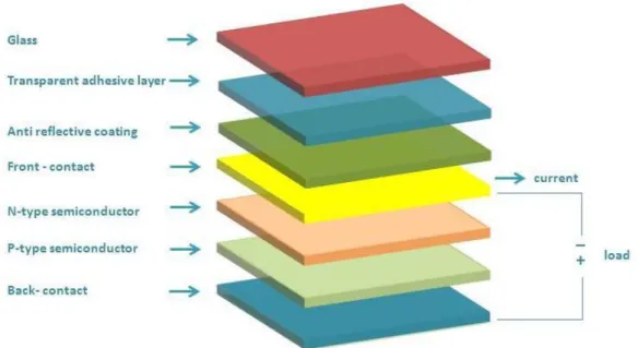
semiconductor absorbing layers of the solar cell. In these layers photons excite electrons from the valence band to the conduction band by absorption of the energetic photon. Excited electrons leave holes behind in the valence band. After charge separation charges are collected at the contacts to produce a current in the circuit. A schematic of a solar cell module is shown in Fig. 1.1 [3].
Figure 1. 1: Schematic of solar cell
A solar cell module includes layers with different properties. Energy conversion occurs in the region of p- and n-type semiconductor junction Carriers diffuse and drift until they reach the contacts. R Recombination of carriers may also take place leading to loss of free carriers and reducing efficiency [3].
For all solar cell modules, conversion process is very similar but efficiency and cost per module are typically different. The efficiency of solar cells suffers from loss mechanisms which were theoretically investigated after Shockley and Quessier’s studies. In 1961, they published a paper on the theoretical performance limits of a solar cell, called the Shockley-Quessier limit. Their work was about an upper
3
theoretical limit of efficiency for a single p-n junction solar cell. Their calculation for a semiconductor with a band gap of 1.34 eV, gives 33.7% efficiency under AM 1.5 solar spectrum. In brief, the maximum power attainable from such a solar cell is 337 W/m² when 1000 W/m² of solar radiation is inducement. In the case of silicon solar cell the efficiency falls down to 29% due to reduced band gap.
Following these initial studies solar cells, have evolved as first, second and third generation solar cells. There is an improvement after each generation but many of commercial solar cells are still first generation. First generation solar cells are silicon based cells and 90% of the cells that one comes across are of this type. Most of the cost for this type of solar cells is due to material costs. Early encapsulating materials, wafers and also cover elements were expensive but after a lot of research, a 70% reduction of cost was achieved after 1997 [4].
1.1. First Generation Solar Cells
Most of commercial solar cells are first generation solar cells made of silicon. Silicon is a well known material used extensively in microelectronics industry. Silicon is an indirect band gap semiconductor and hence absorption and emission of light in Si is inefficient when compared with direct band gap semiconductors. Despite low efficiencies Si has been the material of choice because of its well known properties and relatively low cost. However, when wafer based crystalline silicon is a used material cost dominate the total cost of the solar cell. [5]. Bulk crystalline silicon material cost is about 40% of the cell module [6]. First generation solar cells can be entitled as monocrystalline, polycrystalline, amorphous and hybrid silicon solar cells.
4
1.2. Second Generation Solar Cells
Thin film solar cells emerged for more efficiency and with aim of lowering material costs. Due to their thin film nature, they not only reduce the consumption of materials but also reduce the volume of the cell using materials like CdTe, CdS, CuIn, and GaSe2. The performance of these materials is competitive with first
generation solar cells. Reducing recombination and using good carrier collection approaches, efficiency is improved. However some problems occur when the thickness of semiconductor layer is reduced. Total absorption also decreases. Thin film solar cell technology reduces the active layer thickness [7]. Absorber layer is in the range of 1 µm. To increase the absorption, light trapping techniques can be used applying a pyramidal texture to structure. However, it is not easy to implement such structures onto thin film structures because the thickness is usually smaller than the pyramidal texture to be constructed [6].
Among thin film solar cells, silicon based cells are commercially the mostly available. Silicon based thin film solar cells use s amorphous silicon, microcrystalline silicon and nanocrystalline silicon or combinations thereof [5]. In comparison with solar cells that use microcrystalline silicon, cells that use nanocrystalline silicon reduces reflection increases scattering and diffraction of light [8].
While second generation solar cells increase efficiency and decrease cost, weak absorption near the bandgap edge is still a problem. Hence new solutions are sought after. Using non-toxic materials such as silicon and same thin film processes, new methods are being tried in solar cell technology. These new methods should include ways to surpass Shockley-Queisser limit by using multiple energy band gap structures [9]. Using this approach photovoltaic efficiency can be improved by a factor of 2-3 leading to major cost reduction in per Watt of power [10]. Such multi band gap structures can be called third generation solar cells.
5
1.3. Third Generation Solar Cells
Third generation solar cell technology was developed to overcome both cost and efficiency problems. In comparison with second generation thin film solar cells third generation solar cells promise to reduce cost per watt (below the 0.20/ Wp) [11]. To reach the theoretically expected value, the Shockley-Queisser limit which is a problem for single band gap materials needs to be overcome. Therefore multiple energy level approaches are considered [12, 13].
Multiple band gap approaches lead to a range of concepts that include hot carrier cells, multiple electron-hole pairs cells, multiband cells, up/down conversion cells and finally tandem solar cells. Thermophotovoltaic, thermophotonic devices and quantum antennas are also other approaches to multiple energy systems [10, 11].
When the incident photon energy is much larger than the band gap of the semiconductor involved, the excited carriers such as electrons gain energies high above the conduction band edge. Such carriers are said to be hot carriers. They scatter from phonons to lose their extra energy before the reach the conduction band edge and are said to thermalize during this process. The energy lost to phonons is thermalization losses. Hot carrier cells aim to reduce thermalization losses [10, 11]. A schematic presentation of loss processes is given in Fig. 1.2.
6
Figure 1. 2: Schematic of loss mechanism in single junction solar cell [4, 11]: (1) non- absorption of the photons which have energies less than below the band gap; (2) energy loss due to thermalization; (3) junction loss; (4) contact voltage loss; (5)
recombination loss
By collecting the photoexcited carriers before they cool, more energetic carriers can be collected which gives higher voltage from the cell hence increasing the efficiency. For an imaginary infinite tandem solar cell the limiting efficiency is about to 86.8 % [10, 11]. To approach this limit cooling process should have to slow down sufficiently [4].
Cells that try to make use of multiple electron-hole pair (excitons) work on the principle of electron-hole pair creation. It is possible that multiple carriers are excited as a result of a single high energy photon incident on the solar cell, Fig 1.3. While the details of multiple exciton generation are not well known, it can be said that photon excited high energy carriers can lead to multiple carrier generation. This process can be use to increase efficiency of photovoltaic devices. Research shows that electron-hole pair creation is more efficient in quantum dots instead of bulk materials [10]. A highly energetic carrier can create over seven electron hole pairs [10].Calculated efficiency limit for ideal cells that use impact ionization is about to 85.9 % [4].
7
Figure 1. 3: Schematics of single photon creation of multiple electron-hole pair in a) bulk an in b) nanocrystals [14].
Fig. 1.3 shows photons which have equal or greater than the band gap energy, are absorbed in bulk material and one electron-hole pair is created. These electron-hole pairs have energies close to the bandgap [10, 15-17]. Excitation in a nanocrystal by a highly energetic photon also generates electron-hole pairs, Fig. 1.3[10, 18, 19].
In most solar cells, electronic transitions occur between valance band and conduction band in a semiconductor but an third band (impurity band) allows for more flexibility to design new type of solar cells. With impurity levels low energy photons can also be absorbed. Hence higher efficiencies can be obtained. Impurity band can be adjusted to match photon energy ranges [10]. They can further be extended into multiple numbers of bands, the so called minibands. With an engineering modification, multiple narrow bandgaps and transitions between minibands can also be obtained in semiconductors; this is the working principle of multiband cells, Fig 1.4. Efficiencies of multiband cells are expected to be around 86.8 % for an ideal cell. [4].
8
Figure 1. 4: Schematic of multiband cells [14]
An alternative mechanism to manipulate absorption is the use of up/down conversion is a relatively new method to increase efficiency. Down conversion is an emission process of two low energy photons per high energetic UV photon. Up conversion is the emission of a high energy photon (above the band gap), du to absorption of two low energy photons (below the band gap). Up/down conversion is represented in Fig. 1.5.
Figure 1. 5: Schematic of up / down conversion
The theoretical limiting efficiency is about 36.7 % under one sun. Up conversion materials have the efficiency limit of about 48% under one sun. This limit is higher than down conversion limit due to long energy tail of these materials. A Si solar cell band gap is nearly the same with down converted solar cell [10].
Multijunction solar cells (tandem solar cells) are good examples of third generation photovoltaic devices. These types of cells are applications in which absorption spectrum of semiconductor devices is expanded. They have layer by layer structure
9
with different band gaps. Each layer has its own band gap. In the laboratory, efficiency results are about to 44%. They have the property of high photon absorption and low loss when compared with single- junction solar cells [20]. III-V tandem solar cells are constructed using III-V semiconductors like AlP, GaP, GaAs, and AlSb. IV semiconductor materials are also used in III-V tandem solar cells, Fig 1.6
.
Figure 1. 6: Schematic of III-V solar cell
Further examples of compound solar cells with CIGS (Copper indium gallium selenide) and CdTe/CdS are shown in the Fig. 1.7. Module efficiencies of these structures are 11-13% and 10-12 %, respectively.
10
Figure 1. 7: Schematic of CIGS and CdTe/CdS structures (courtesy of R. Turan)
Currently, the abundance and low material cost of silicon drives the market. a-Si:H solar cells with two or three junctions have demonstrated efficiencies in the laboratory as high as 8.5% and for commercial modules 5.5% [21]. Amorphous silicon-germanium alloys (a-SiGe:H) with two or three junctions has been shown to have laboratory and commercial efficiencies as 13% and 6.3%, respectively [21].
An example of state of the art a-Si/µc –Si-H silicon cells is shown in the Fig. 1.8. Modules made from these cells show efficiencies of 8-10%.
11
Amorphous silicon tandem cells are preferred due to ease of production and low cost. To increase their efficiencies especially in the UV nanocrystalline structures are being considered. Due to reduced crystal size, carriers in the relevant band are confined in a potential well giving the ability to tune the effective band gap. The smaller the crystal size, the larger is the band gap, Fig. 1.9.
Figure 1. 9: Optical gap as a function of nanocrystal diameter [22] (courtesy of C. Bulutay).
It is also possible to dope the nanocrystals for facilitate conduction [23]. Mixed phase structures which are partially amorphous and partially crystalline in the range of few nanometer or few tens of nanometer are also considered nanocrystalline silicon [24]. Solar cells which are constructed with nanostructures are good candidates for efficient solar cells because they include both crystalinity and thin film deposition techniques [25]. Sandwiching nanocrystal silicon layers between [25] layers as SiO2, Si3N4 and SiC electronic minibands can be obtained for electrical
12
There are many ways to form Si or Ge nanocrystals. Typically thin films of Si or Ge rich silicon oxides or silicon nitrides are deposited by sputtering or PECVD at temperatures as low as 100-300 C [24]. Usually this is followed by a thermal treatment in a furnace or a rapid thermal processor to phase separates the Si in the matrix. Multilayer of Si or Ge rich oxides can be deposited, separated by layers of oxides and crystallized. With proper engineering it is possible to generate layers with different sizes of nanocrystals. The layers with smaller sized naoncyrtals absorb the blue part of the spectrum while the red part is absorbed by the larger sized naoncrystals. Such a scheme makes better use of the solar spectrum. A schematic example of the said structure is shown in the Fig. 1.6.
Using band gap engineering, a single layer of semiconductor nanocrystals in an oxide matrix can be used to increase absorption in the ultraviolet-blue part of the spectrum, thereby increasing efficiency. Such a layer can be integrated into existing silicon based solar cells. A major technological challenge to integrate Si or Ge nanocrystals into a solar cell structure is the deposition of Si or Ge rich oxides as well annealing to phase separate and crystallize Si or Ge in the oxide matrix. This is all the more important for thin film solar cell production where large sheets of glass are transported from one deposition chamber into another to deposit multiple layers of a-Si. To have better control and lower costs, low temperature deposition techniques are always preferred. Plasma enhanced chemical vapor deposition (PECVD) or RF sputtering techniques lend themselves to low temperature deposition. However, formation of Si or Ge nanocrystals require high temperature, 1100 C for 1 hour and 900 C for 1 hour are typical for Si and Ge nanocrystals. For a typical 2x3 m2 thin film panel, this is a very large thermal budget. Such high temperatures, not only increase cost but also is detrimental to the solar cell due possible interface diffusion between different layers. A possible solution is to use laser induced crystallization of Si or Ge in the oxide matrix. With proper choice of wavelength and therefore absorption, it may be possible to locally heat the Si or Ge rich layer to induce
13
crystallization of Si or Ge. This may not only generate nanocrystals but also lower the thermal budget over which the panel undergoes, therefore lower costs.
In this study, our aim is to study the formation of silicon and germanium nanocrystals by annealing SiOx:Ge alloys with a continuous wave Ar+ laser. We
grow SiOx:Ge thin films on quartz and infrared transmissive silicon substrates with PECVD. Than composition analysis by RBS, FTIR and ellipsometry were done on as-grown samples. This was followed by laser processing these samples of thin films into ~15 micrometer parallel lines by various power densities. Characterization of annealed samples began with Raman spectroscopy. In Raman results germanium crystal peaks were observed at ~300 cm-1. Raman spectroscopy with surface profile analysis shape, size and growth distributions of the particles were determined. This study suggests that it is possible to form Ge nanocrystals in oxide matrices with CW laser annealing, for an efficient layer for third generation tandem solar cells.
14
Chapter 2
Experimental
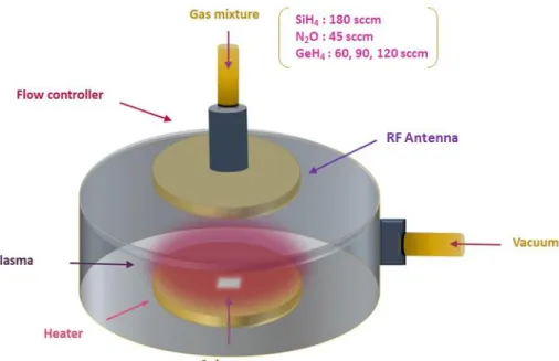
In this chapter preparation of samples with the Plasma Enhanced Chemical Vapor Deposition (PECVD) and laser processing by continuous wave Ar+ ion laser will be explained. We also summarized measurement techniques used in this thesis. A brief explanation of the analysis techniques such as absorption and Raman Spectroscopy, Ellipsometry, Rutherford Backscattering and Surface Profile analysis are given.
2.1 Sample Preparation
Quartz wafers were cut into as 1x1 cm sizes in the clean room. Afterwards three pieces of silicon and quartz were cleaned as follows:
First, acetone followed by isopropanol and DI water bath was applied to silicon and quartz pieces. Samples were then dried with pure nitrogen gas. Then, thin film deposition onto clean silicon and quartz were applied. SiOx:Ge thin films deposited
using the PECVD method. This technique was preferred due to low temperatures used in thin film deposition as well as relatively easy adjustment of thin film compositions. Temperatures used are typically between 200 oC - 300 oC. For our study, the substrate temperature was set to 250 o C. The thin film deposition process begins with the gas mixture of (2% SiH4: %98 H2, 2% GeH4: %98 H2 ) flowing
15 Sample Code Flow Rate (sccm) Power (W) Pressure (Torr) Temperature (o C) Time (min) 2% SiH4 in H2 N2O 2% GeH4 in H2 A 180 45 60 12 1 250 10 B 180 45 90 12 1 250 10 C 180 45 120 12 1 250 10
Table 2. 1: List of samples prepared by PECVD
Gas mixture flows down from the shower head with high uniformity through the upper plate which is also an electrode. Flow rate is adjusted by mass flow controllers. Upper plate has an RF antenna which transmits radio waves at 13.56 MHz. RF waves ionize the gas mixture and ionized gas creates a plasma between upper and lower plates. Lower plate is a grounded electrode. Lower plate is heated to speed up the chemical reaction of adsorbed species on the substrate. All these steps have to be in a vacuum-operated chamber. Vacuum requirements are satisfied by roots pump and mechanical pump that controlled by pressure controllers. Pressure is generally set at about 1 Torr. To obtain a clean process, before the deposition, substrate should be cleaned by oxygen plasma in a vacuumed chamber at 10-5 pressure. After the cleaning, thin film deposition is directly related to the time from now on RF power is
16
switch on. RF power was set to 12 Watt and conclusion of the process 500 nm thick thin films were obtained successfully. A schematic of PECVD is shown in Fig. 2.1.
Figure 2. 1: Schematics of the PECVD reactor
2.2 Laser Processing
Annealing process is required to transition of amorphous Ge into Ge crystals. In this study a CW Ar+ laser was used to process the samples. Laser annealing is preferable when compared with thermal annealing because of the ability to locally heat, micron range pattern formation ability, and easier annealing process for wider layers of films. Also Raman characterizations can be done on the same setup.
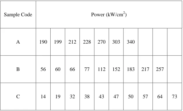
In this work three types of samples were annealed with different power densities. These power densities are shown in Table 2.2.
17
Sample Code Power (kW/cm2)
A 190 199 212 228 270 303 340
B 56 60 66 77 112 152 183 217 257
C 14 19 32 38 43 47 50 57 64 73
Table 2. 2: Annealing power densities per unit cm2
The laser processing took place as follows:
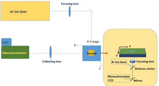
The optical path during laser irradiation with the 488 nm line of the CW Ar + laser is shown in Fig. 2.2. In this path the light passed through two mirrors of the microscope. One of the mirrors was dichroic which reflects only 488 nm radiation and transmits longer wavelengths. Dichroic mirror directed the reflected light to a focusing (x4) lens and transmitted light to a lens in front of the monochromator.
18
Figure 2. 2: Schematic of laser processing setup
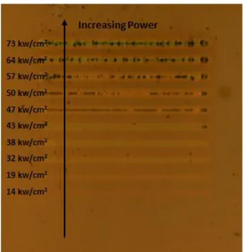
The samples were scanned under 488 nm reflected beam by a computer controlled XY stage that is placed on top of the focusing lens. Dwell times (line width/scan speed) are 0.32s, 0.4s and 0.5s for sample A, B and C, respectively. The optical image of the scanned sample was taken by an in-situ camera on same setup as Fig. 2.3. Therefore irradiated lines could be followed systematically.
19
Figure 2. 3: An optical microscopy image of laser processed lines with increasing powers.
As it is seen from the Fig. 2.3 irradiated lines show different color characteristics. This suggests that for different powers, changes in the refractive index and topology have taken place. There is a threshold power over which the effects of irradiation have become visible have been determined with Raman spectroscopy. Threshold power densities and Ge concentrations in Table 2.3 shows the relation between needed power densities for crystal formation for each sample. Crystal formation will be discussed in following chapter.
20 Sample
Code
Threshold power density (kW/cm2)
GeH4 flow rate
(sscm)
A 199± 2 60
B 60± 2 90
C 38± 2 120
Table 2. 3: Nanocrystal formation power density threshold for laser scanned samples
2.3 Measurement Techniques
2.3.1 Absorption Spectroscopy
Fourier Transform Infrared (FTIR) Spectroscopy is a technique which is used to obtain absorption, transmission and reflection spectra of samples in many phases as solids, liquids or gasses in a wide spectral range (UV-Visible). A Fourier Transform Spectrometer works in principle of Fourier transformation. Raw data which are collected over a wide spectral range are converted into a spectral data by software. Fourier transform is a mathematical process.
21
Figure 2. 4: Schematic of a Fourier Transform Infrared Spectroscopy setup
As is represented in Fig. 2.4, a FTIR setup consists of a light source, an interferometer, a beam splitter, mirrors and detector. A broadband light source which can emit large range of wavelengths emits light onto Michelson interferometer that consists of two mirrors, a beam splitter and a compensator. One of the mirrors is fixed and the other is movable. If only a monochromatic beam is present in the system, as the mirror moves, the intensity on the detector is modulated due to interference of the monochromatic beams reflecting from the fixed and moving mirror. When the two beams are in phase at a given position of the moving mirror, there is constructive interference while when the mirror moves and the beams are out of phase and destructive interference takes place on the detector with minimum intensity of light falling on it. The resulting signal is sinusoidal. When there are two monochromatic beams in the optical path, these two beams interfere with an additional feature appearing, if an absorber is present in the optical path, Fig.2.5 and Fig 2.6. The interfering signal is called an interferogram. The signal to be measured
22
is recovered using the equation: where I(z) is the interferogram.
Figure 2. 5: Interferogram of two monochromatic sources
Figure 2. 6: Interferogram of five monochromatic sources.
In an actual Fourier Transform Infrared spectrometer the light source is a broad band source, a blackbody. The source is then modulated by the Planck distribution
23
function and is effectively included in the interferogram function I(z). Molecules in the sample can be regarded as oscillators. If the frequency of incoming light matches with the frequency of oscillators light is absorbed, an effect known as resonance. Absorbed light recorded in the interferogram and is detected by detector. When a large number of oscillators are present, the spectrum contains absorption data for different wavelengths. A sample FTIR spectrum for reflectance of SiOx:Ge sample is
given in Fig. 2.7.
Figure 2. 7: A sample for reflectance spectrum of SiOx:Ge sample
Using collected spectra, vibrational bonds of a sample can be determined. PeakFit software can be used for analyzing the data.
2.3.2 Raman Spectroscopy
Raman spectroscopy is a technique to measure vibrational, rotational and other low frequency modes of a system. It is an inelastic scattering of light from UV, VIS or NIR laser sources. When applied to solids, phonon Raman scattering allows the
24
determination of vibrational frequencies of phonon modes. Incoming light scatters from semiconductor crystal resulting in the determination of the relevant phonon modes. Briefly, Raman scattering can be described as: An incident photon excites an electron in an initial state into an intermediate state |a> and generates an electron-hole pair. Electron-electron-hole pair emits a phonon while it is scattered into another state, |b>. Electron-hole pair recombines and emits the scattered photon. Scattering process can be occur as Stokes and anti-Stokes Raman where a phonon is created or annihilated, respectively [26].
The macroscopic theory of Raman scattering can be described assuming a sinusoidal electromagnetic wave is present in a medium given by
(2.1)
induces a sinusoidal polarization :
(2.2)
Frequency and wavevector of induced polarization is same as incident radiation when is described by
(2.3)
denotes electric susceptibility of medium, and represent wavevector and frequency of incident radiation.
There are some fluctuations in susceptibility because of thermally excited atomic vibrations if the medium has a finite temperature. It can be said that phonons are
25
quantized atomic vibrations in crystalline semiconductors. Phonons can be represented in terms of atomic displacements as:
(2.4)
which has wavevector and frequency . Using adiabatic approximation in which electronic frequencies are much larger than , can be taken as a function of atomic displacements and it can be expand as a Taylor series in as follows
(2.5)
first term with denotes no fluctuation in medium with electric susceptibility. Second term expresses induced oscillating susceptibility by atomic displacements.
Polarization of the medium with atomic vibrations can be represented by using (2.5) into (2.3) as follows
(2.6)
is the vibrating polarization which is in phase with incident radiation and
induced polarization by phonon.
(2.7)
26
(2.8)
cos[( ) } cos[( ) ]} (2.9)
Stokes and anti-Stokes scattered lights have wavevectors = ( ) and
( ) and frequencies and respectively. As it is represented in equations an incident photon with is absorbed by material and energy of incident photon is used for phonon creation. Then a photon is emitted with frequency represented as . This process is called Stokes scattering. Otherwise an incident photon gains energy from material after scattering therefore emitted photon has a new frequency as this is called anti-Stokes
scattering. Difference between scattered and incident light frequencies is named as Raman shift [26].
To perform a Raman experiment a setup includes the elements which are shown in Fig. 2.8.
27
Figure 2. 8: Schematic diagram of Raman experiment
A monochromatic light from a laser is focused on the sample with mirrors and focusing lenses. After Raman scattering, scattered light is collected using a collection lens. Collimated light is focused onto the slits on monochromator. Light reaches the grating which is in the monochromator and dispersed into its components. The last step is the measurement by CCD to identify the wavelengths of the signals. An example of a Raman signal is shown in Fig. 2.9 [27].
28
Figure 2. 9: A typical Raman Spectrum of annealed SiOx:Ge sample
2.3.3 Ellipsometric Analysis
Ellipsometry is a method which is used to acquire the optical properties of thin films and bulk materials. These properties are complex index of refraction, extinction coefficient and also film thickness for thin films. An ellipsometry setup includes light source which can be laser, xenon gas discharge or quartz-halojen lamp, a polarizer, an analyzer and a detector Fig. 2.10.
29
Figure 2. 10: Schematic diagram of ellipsometry
Incident light which comes from light source pass through the polarizer which is a linear polarizer then crashes into the sample and reflects, reflected light has a phase shift between its s and p components therefore it turns to elliptically polarized light. Then light comes into analyzer which is another linearly polarizer and becomes a linearly polarized light afterward it is collected by detector. All the measurement can be done in different analyzer-polarizer angles and in this case obtained information represents different intensities in various angles. After data analysis of detector, s and p polarization ratio is determined. Owing to this ratio two parameters as Ψ and Δ can be calculated with the equation below.
(2.10)
Ip is the incoming light intensity and Is is the reflected intensity of p and s polarized
light respectively. They come from Fresnel equations for polarized light which is in boundaries in planar multilayered samples. To determine the refractive index and extinction coefficient or thickness of the thin film, analyzing software is required. Software fits theoretical Ψ and Δ values to experimental data by minimizing root-mean-square value. The root mean square error is calculated as follows:
30 (2.11)
For data fitting, a model should be constructed which is applicable for the structure of the film. In this model, the layers with different thicknesses and refractive indices are represented. The dielectric constants of the layers are represented with models of oscillator systems such as Lorentz oscillator or Cauchy model etc. Both the real part and the imaginary paert of the refractive index can be found using the constructed model parameters and some formulas (Snell’s Law, Fresnel Equations, thin film interference expression) [28]. Software compares generated and experimental datas with each other to adjust the fit parameters of physical model by minimizing the difference. A typical elipsometric data is shown in Fig. 2.11.
31
2.3.4 Rutherford Backscattering Technique
Rutherford Backscattering Spectroscopy is a nuclear technique which is used for near surface analysis by ions. In this technique a target is bombarded by accelerated ions and an elastic scattering is observed between the bombarded sample and incident ions, after scattering, projectile ions are detected at backscattering angles about 150o -170o [29].Schematic is shown in Fig. 2.12. Alphas particles (He+2) or protons with energies in the range of 1-4 MeV are preferred for elastic Coulomb scattering. Incident ions are scattered with higher energies from heavier elements of the target when compared with lighter elements. A surface barrier detector measures the energy of the backscattered ions to determine the sample composition and thickness. Taking energy and momentum conservation into consideration the scattered particle has the energy represented by :
2.12
and is known as kinematic factor. Here m1 is the mass of the incident ion while m2 is
the mass of the target atom. Taking the differential backscattering cross section and the energy loss per unit thickness expressed as stopping power , a model can be fitted to data to determine the sought after variables.
32
Figure 2. 12: Schematics of Rutherford Backscattering experiment
Rutherford Backscattering Spectroscopy is used for quantative data about composition of sample or depth profiling of independent ingredients. Accessible depth is in the range of several microns as 1-10 microns.This depth is about 2 um in the case of He+2 bombardment, specifically [29]. A typical Rutherford Backscattering data is given in Fig. 2.13.
33
Figure 2. 13: A typical RBS data.
2.3.5 Surface Profile Analysis
Surface profile analysis is a method which determines the local deviations of the surface and obtains surface texture. Surface texture analyzing is important for reliabity of the manufacturing method and checking the resulting of the experimental process. Surface profilometer makes a stylus-based measurement. It is consist of a mechanical stylus which is coupled with Linear Variable Differential Transformer (LVDT) and a moving stage. Sample is located on the moving stage, while precision stage is moving stylus scans the surface and detects roughness. LVDT converts this texture information to an analog signal which corresponds to vertical movement of stylus [30].
34
Figure 2. 14: A sample surface profilometer image
In Fig. 2.14 the movement of stylus is represented as a graph of vertical movement vs. deeps and tops of surface. X axis represents vertical movement of stylus and Y axis shows the surface roughness profile of the sample.
35
Chapter 3
Results
3.1 Characterization of As-Grown Samples
3.1.1 Composition Analysis
The RBS analysis presented here were done at CNR-IMM (Consiglio Nazionale delle Ricerche - Istituto per la Microelettronica e Microsistemi) by S. Mirabella. The analysis was carried out using 2.0 MeV He+ beam. Backscattered He+ particles were detected at 15º with respect to the incident beam. The beam current varied between 90-120 nA with total detected charge being 30-90 µC. The RBS data in Fig 3.1 shows the spectra for three as-grown samples with different Ge concentrations. All spectra have similar character. The backscattered He+ particles have the highest energy when they scatter from the heaviest atom in the matrix, in this case Ge. This is followed by backscattering from Si (of SiO2 matrix) with the Si edge being at
about 1.2 MeV. The light elements of O and N cause backscattering yet still lower energies which when compounded by the thickness of the SiOx:Ge films gets mixed
up in the continuum of the spectra below 1.0 MeV. The experimental data were then fit using a simulation program to extract composition and thickness information about the as grown SiOx:Ge samples. In the RBS analysis, only Si, Ge and O atom doses were determined directly (typically in E15at/cm2), while N and H concentrations were inserted into the fit program to just give satisfactory fit to the data otherwise, if no N or H is considered, the simulation does not fit the spectrum. This causes a large error in the N and H amount. Being a very light element, the best
36
way to analyze H is to use elastic recoil detection technique, which was not available for this work. RBS spectra for as-grown SiOx:Ge samples are given in Fig. 3.1.
Figure 3. 1: RBS spectrum of as-grown SiOx:Ge samples
Using the data which are in graph above simulations was done for the film and the substrate. Due to very weak signal of N, extracted composition after simulation was affected by relatively large errors for N, but Si and O data are obtained with small errors. As the software estimates the energy loss as a function of the composition, the errors on N can have negative drawbacks also on Si and O. Typically the simulation was able to fit RBS down to channel 180 with relative ease. Simulations are given in Fig. 3.2 for samples A, B and C, respectively.
37
Figure 3. 2: Simulations and experimental RBS data for samples A, B and C, respectively.
RBS spectra does not yield immediate thickness information but only dose (in 1015 at/cm2) of the elements. If the density can be measured independently, then the dose data can be converted to thickness. An average of 6.99x10²² at/cm3 can be used for SiO2 density. However, this is not strictly valid in the case of SiO2 depositions made
with plasma enhanced chemical vapor deposition techniques. Table 3.1. shows the results of the simulations of the data shown above. H dose for samples A,B and C were determined in an indirect way, hence the relative error is large. The errors for N
38
and H doses affected the composition results in percentage. But Si and O and their ratios are mostly accurate.
Sample Si Ge O N H Total t x1015 (at/cm2) (%) x1015 (at/cm2) (%) x1015 (at/cm2) (%) x1015 (at/cm2) (%) x1015 (at/cm2) (%) x1015 (at/cm2) (%) (nm) A_as-grown 620 21 230 7.7 1400 47 190 6 550 18 2990 433 B_as-grown 510 20 310 12 1100 44 50 2 550 22 2520 365 C_as-grown 500 18 440 16 1200 43 180 6 500 18 2820 409
Table 3. 1: Si, Ge, O, N and H doses and thickness results with respect to simulation data of RBS
Silicon concentrations of as-grown A, B and C samples respectively are 21%, 20% and 18%. Germanium concentrations are inversely proportional to included Silicon dose. Percentage values are 7.7% for as-grown A, 12% for as-grown B and 16% for
39
as-grown C. Oxygen has the huge portion of the content for all samples. The values are 47%, 44%, 43% for A, B and C, respectively. The data is shown in Fig. 3.3. The effect of GeH4 flow rate is clearly seen. Increasing flow rate increases the Ge
concentration in the SiOx:Ge thin films while the effect on Si and O concentration is
minimal. Increasing Ge concentration causes a small decrease in both Si and O in the thin films suggesting that Ge consumes some of the O in Ge-O bonds. Nitrogen concentration due to NH3 is quite portion of SiOx:Ge films. Percentage values vary
as 6% for A, 2% for B and 6% for C. Also hydrogen doses are 18%, 22% and 18% for A, B and C, respectively.
Fig. 3. 3: RBS concentrations of Ge, Si and O for different GeH4 flow rates.
3.1.2 Absorption Spectroscopy Analysis
Absorption spectroscopy analysis was done using Fourier Transform Infrared Spectroscopy. Reflectance was measured for each as-grown thin film which was deposited on quartz and Si substrates. Measurements were done for range of 400-4000 cm-1 interval with 6mm aperture setting, 10 kHz scanner velocity, 8 cm-1 resolution and 2048 scan time. KBr beam splitter and RT-DLaTGS detectors were
40
preferred because of convenience for mid-infrared measurements. As-grown thin films on quartz substrates, as-grown thin films on Si substrates were measured using quartz substrate as reference Fig.3.4.
Figure 3. 4: Reflectance measurement of empty quartz
Si-Si stretching bonds were determined at 786 cm-1 and 942 cm-1 also Si-O-Si stretching bonds with 1086 cm-1, 1124 cm-1, 1190 cm-1 and 1243 cm-1 with central frequencies are shown in Fig. 3.4
After reflectance measurements the data was analyzed using PeakFit software go determine selected vibrational bonding. In this analysis, the peaks were fit using Voigt function and residuals method was used. Bonding identification was done as below in Fig. 3.5.
41
Figure 3. 5: Comparative reflectance measurements of, as-grown quartz for samples A (60 sccm GeH4), B (90 sccm GeH4), and C (120 sccm GeH4)
For as grown samples Ge-O-Ge symmetric and asymmetric stretching bonds were identified at 816 cm-1 and 1055 cm-1, respectively. In addition to Ge-O bands Si-O stretching bands was determined 1148 cm-1 and 1283 cm-1 with central frequencies.
3.1.3 Refractive Index Measurements
Refractive indices of samples A, B and C were determined using ellipsometry measurements. J. A. Woollam variable angle spectroscopic ellipsometer [31] was used for measurement. The wavelength interval of 300-1700 nm was chosen. Angle of incidence was adjusted between 65-75 degrees. Typically data at 65º, 70º and 75º
42
were taken. Experimental Ψ and Δ datas were obtained as in Fig. 3.6 for each sample.
43
Figure 3. 6: Raw ellipsometric data for three SiOx:Ge samples
To determine refractive index and extinction coefficient, there we use the software program WVASE 32. Software fits the experimental data to model generated datas which are calculated with respect to a constructed model. Using the most proper model for fitting provides the best fit between the experimental and model dependent data. The model consists of layers of materials known or suspected to be in the sample tested. The refractive index values for the layers in the model structure . Already defined models in software can be used also. Cauchy model is one of them. In terms of the Cauchy model, materials used in the molde can be dielectrics, semiconductors but not metals. In teh Cauchy model refractive index and the extinction coefficient as a function of wavelength is given as:
44
(3.2)
For this equation represents index of refraction and symbolizes extinction coefficient as a function of function .
Raw data was fitted by software and refraction index, extinction coefficients and also film thicknesses for thin film samples were obtained. Constructed models for samples A, B and C are given in Fig. 3.7.
Figure 3. 7: Fitting models of ellipsometric data of SiOx:Ge samples.
Hence conformity could be achieved for raw and theoretical data. After fit operation using the constructed model, fitted data of Ψ and Δ were obtained as Fig. 3.8.
45
46
Refractive index and extinction coefficient were obtained after data fitting of Cauchy model to experimental data. Calculated refractive indices are given in Fig. 3.9. As is shown in the Fig. 3.9, the refractive indices of all samples decrease as a function of wavelength as is expected of a Cauchy model. The increasing concentration of Ge increases the overall refractive index shifting the curves to higher index values. This is also expected as Ge has a large index of refraction. The corresponding extinction and absorption coefficients increase as the wavelengths decrease towards UV, Fig. 3.10 inset. Increasing Ge concentration also increases the extinction coefficient in the UV part of the spectrum.
Figure 3. 9: Refractive indices of three SiOx:Ge samples for A (60 sccm GeH4), B
47
Figure 3. 10: Absorption and extinction coefficients of SiOx:Ge samples for A (60
sccm GeH4), B (90 sccm GeH4), and C (120 sccm GeH4).
Absorption coefficient at a given wavelength can be calculated from the extinction coefficient using the formula given below.
(3.3)
The absorption coefficients are determined using the formula 3.3 are shown in Fig. 3.10. As would be expected, absorption coefficients also increase with increasing Ge concentration.
Film thicknesses can be determined using ellipsometric measurements as was previously mentioned. The thicknesses of the samples deposited by PECVD process
48
and the results of the measurements performed with ellipsometry match with RBS analysis, discrepancy being proportionally to increasing Ge concentration.
3.2 Characterization of Processed Samples
3.2.1 Crystallization of Ge in SiO
xmatrix
After CW laser processing the as-grown samples, several characterization methods are used to determine to characterize the modifications that take place in the samples. The central theme of this research is to see whether Ge in SiOx can be induced to
crystallize using CW laser irradiation. Raman spectroscopy is an ideal tool to determine whether Ge crystallization takes place in the SiOx matrix, as Raman
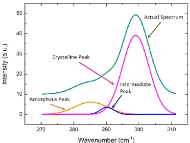
phonon scattering requires the presence of an orderly crystal. We used this method to determine the Ge crystal formation after irradiation of SiOx:Ge thin films with Ar +
laser. Crystalline Ge has a well known optical phonon peak that is located at ~300 cm-1 [32]. Therefore, we study the phonon Raman scattering from CW laser irradiated samples as a function of irradiance in W/cm2 and expected to observe a peak which in the vicinity of ~300 cm-1 to verify the Ge crystallization. As it is seen in Fig. 3.11, Fig. 3.12 and 3.13, for each sets of samples crystalline Ge Raman peak was observed above a threshold value of irradiance.
49
Figure 3. 11: Raman Ge crystal peaks of annealed A series by various powers (linear scale).
Fig. 3.10 shows the Raman spectra of different spots irradiated with different power densities. It is clear from Fig. 3.10 (left) that at power densities less than 199 kW/cm2, the laser irradiation does not cause any Ge signal. The spectra of quartz and as grown samples should be noted as comparison. At 199 kW/cm2 there is a sudden appearance a strong Ge peak close to 300 cm-1. We suggest that laser power density induces phase separation and formation of Ge nanocrystals in the SiOx. This peak is
quite sharp with a tail towards low frequencies indicating the presence of smaller size nanocrystals, understood in the context of size distribution. Further increase in power density further sharps the peak, eliminates the low frequency tail and shifts the peak towards high frequencies. At 304 kW/cm2 the Ge peak located at 300cm-1.
Raman scattering in samples with higher concentrations of Ge is illustrated in Fig. 3.11. A significant note is the amount of power density required to irradiate these samples which is much less than those in Fig. 3.10. The reason for this is the increasing absorption of the laser beam due to increased Ge concentration. It is clear from the sets of data in Fig. 3.11, that at power densities less than 60 kW/cm2 the laser beam does not cause the appearance of a Ge signal. At 60 kW/cm2, there is budding appearance of Ge signal overlaying the background. This allows us to
50
identify the crystallization threshold as 60 kW/cm2. Increasing the power density further sharpens the Raman peak and at 257 kW/cm2 reaches to its final form.
Figure 3. 12: Raman Ge crystal peaks of laser irradiated B series by various power densities (linear scale).
51
Figure 3. 13: Raman Ge crystal peaks of laser irradiated C series by various power densities (linear scale).
Samples irradiated with different laser power densities to identify crystallization threshold, Fig. 3.14. As is expected, below the threshold power density, there is no crystalline Ge peak but above the threshold power density nanocrystal formation is clearly observed. For each set of samples, Raman spectra of samples A, B, C irradiated at the threshold laser power densities are summarized in Fig. 3.13. Only in sample A with the lowest Ge concentration has a sudden transition to crystallization. While there is no effect of laser irradiation at 190 kW/cm2 there is a clearly sharp Raman peak at 199 kW/cm2. This may be due to low absorption of this sample at the wavelength of laser irradiation.
52
Figure 3. 14: Threshold power densities for crystallization of A (60 sccm GeH4), B
(90 sccm GeH4), and C (120 sccm GeH4) (linear scale).
3.2.2 Surface Topography
Surface topography of annealed SiOx:Ge samples were studied using a Dektak stylus
profiler. A stylus scanned the samples step by step for each irradiated line and recorded all the profile. Our samples were scanned along 50 µm range by surface profiler. Surface profile scans as a function of irradiation power density are given below for three samples labeled A, B, C.
53
Surface profiles of A Series
Figure 3. 15: Surface profile analysis for A series by various annealing powers.
It is clear from the above data that at low power density of 190 kW/cm2 there is a small depression at the center of irradiation. This is most likely due to composition of the thin film. PECVD deposited thin films are known to have voids which are annealed out to create a depression during irradiation. However at higher laser intensities, the profile becomes very complex. The profile may involve softening of the oxide layer along with evaporation. The profile seems to imply mass transport of material along the hot surface. Topography showed varying depths from 15 nm to 25 nm and up to peak magnitudesbetween 5-160 nm for A series.
54
Surface profile of B Series
Figure 3. 16: Surface profile analysis for B series with various laser power densities.
The optical absorption for sample B is more than sample A. This reduces the laser power density required to irradiate the sample. At the threshold laser power density the small depression in the profile is typical, Fig. 3.16. Only at higher laser power density of 77 kW/cm2 do we see a small protrusion in the middle of the depression.
55
Surface profile of C series
56
C series surface profile graphs give similar information as A and B series graphs. In summary, laser irradiation changes the surface profile of the surface. Irradiation is accompanied with depression as well as bulging due to redistribution of mass during irradiation. Higher Ge concentration makes the crystal formation easier. This means crystallization occurs at lower power densities for higher Ge concentrations. While the onset of crystal formation is e at 190 kW/cm2 for sample A, it occurs below 60 kW/cm2 and 31 kW/cm2 for samples B and C, respectively.
3.2.3 Vibrational Modes and Bonding
Fourier Transform Infrared (FTIR) Spectroscopy for processed samples were applied to samples which were annealed with three different power densities. In these measurements, due to absorption property of quartz in our studied region we couldn’t measured a reasonable spectra for processed samples with quartz reference. Therefore Au was used as reference instead of quartz. Outcome of measurements represented the quartz and SiGeO thin film bonds together. FTIR reflectance spectras for different power densities are given in Fig. 3.18-20 for each set of samples.
57
Figure 3. 18: Reflectance measurements of laser processed A (60 sccm. GeH4) series
58
Figure 3. 19: Reflectance measurements of laser processed B (90 sccm GeH4) series
59
Figure 3. 20: Reflectance measurements of laser processed C (120 sccm. GeH4)
series (linear scale).
As it is shown in Fig. 3.18 same bonds were determined for each power densities. Peaks at ~786 cm-1,~ 942 cm-1, ~1190 cm-1 and ~1243 cm-1 are the identified quartz peaks in Fig. 3.4.
60
Figure 3. 21: Comparative reflectance measurements of laser processed A (60 sccm. GeH4), B (90 sccm GeH4), C (120 sccm GeH4) series (linear scale).
Fig 3.21 represents the comparison of reflectance spectras for different GeH4
concentrated samples. As it is seen from figures, peaks shift to lower wavenumbers with respect to higher power densities and GeH4 concentrations. It is the result of
construction of heavier atom bondings. Observed peaks can be identified as ~726 cm
-1
Ge-O stretching [33], ~866 cm-1 Ge-O-Ge asymmetric stretching [34], ~1040 cm-1 Si-O-Si asymmetric stretching [34] and ~1140 cm-1 Si-O stretching [35] which are come from thin film. With annealing process, more Ge atom makes new bonds with Ge or other atoms which are included within thin films. We didn’t observe the Ge-Ge peaks because of our studied spectral region didn’t include lower wavenumbers where Ge-Ge bonds appears at.
61
Chapter 4
Conclusions and Future Works
In this thesis, we fabricated Ge doped silicon oxide films by using plasma enhanced chemical vapor deposition technique. Three type of thin film was made by different gas flow rates. Gasses which are used in deposition process are GeH4:H2, SiH4: H2,
N2O. Using different GeH4:H2 concentrations, films were obtained with various
properties.
After deposition process, compositional analysis was performed for samples. Using Rutherford Backscattering method and its simulations Si, Ge, O, N and H doses within samples were determined. Also thicknesses of thin films were estimated assuming the SiO2 density.
For complex refractive index, extinction coefficient and thickness determination, we performed Ellipsometry analysis with three angle of incidence as 65o, 70o and 75o. We measured Ψ and Δ raw data then using software and constructing a proper model to characteristics of samples we fit these raw data to generated data. (Cauchy model was used for data fitting). Therefore complex refractive index and extinction coefficient were calculated. Obtained results were showed that increasing Ge concentration is proportional to increasing of refractive index and also extinction coefficient. All these fit processes were performed for each of the samples.
![Figure 1. 2: Schematic of loss mechanism in single junction solar cell [4, 11]: (1) non- absorption of the photons which have energies less than below the band gap;](https://thumb-eu.123doks.com/thumbv2/9libnet/5755921.116308/15.892.244.721.176.410/figure-schematic-mechanism-single-junction-absorption-photons-energies.webp)
![Figure 1. 9: Optical gap as a function of nanocrystal diameter [22] (courtesy of C.](https://thumb-eu.123doks.com/thumbv2/9libnet/5755921.116308/20.892.263.693.335.670/figure-optical-gap-function-nanocrystal-diameter-courtesy-c.webp)