EXCITONICS OF COLLOIDAL
NANOCRYSTALS FOR NEXT-GENERATION
OPTOELECTRONICS
a dissertation submitted to
the graduate school of engineering and science
of bilkent university
in partial fulfillment of the requirements for
the degree of
doctor of philosophy
in
electrical and electronics engineering
By
Burak G¨
uzelt¨
urk
May 2016
EXCITONICS OF COLLOIDAL NANOCRYSTALS FOR NEXT-GENERATION OPTOELECTRONICS
By Burak G¨uzelt¨urk May 2016
We certify that we have read this dissertation and that in our opinion it is fully adequate, in scope and in quality, as a dissertation for the degree of Doctor of Philosophy.
Hilmi Volkan Demir(Advisor)
Ayhan Altınta¸s
Mehmet Z. Baykara
Alphan Sennaro˘glu
Ra¸sit Turan
Approved for the Graduate School of Engineering and Science:
Levent Onural
Director of the Graduate School ii
ABSTRACT
EXCITONICS OF COLLOIDAL NANOCRYSTALS FOR
NEXT-GENERATION OPTOELECTRONICS
Burak G¨uzelt¨urk
Ph.D. in Electrical and Electronics Engineering Advisor: Hilmi Volkan Demir
May 2016
Owing to the tremendous progress in the past decade, semiconductor nanocrys-tals that are grown by low-temperature solution-phase epitaxy have evolved into highly promising material systems for optoelectronics with ever increasing inter-est from the industry. However, fundamental challenges exist in conventional nanocrystals hampering their energy-efficient optoelectronic devices. In this the-sis, we addressed important scientific problems and overcome various technologi-cal hurdles through optitechnologi-cal physics discoveries and innovative nanomaterial pro-cessing. Specifically, we have proposed, designed and developed next generation of nanocrystals that exhibit superior optical and material properties than those of the conventional nanocrystals. Mastering intra- and inter-particle excitonic pro-cesses in these nanocrystals and their hybrids empowered us to control and tailor the desired photonic response. Our key achievements include demonstration of record high modal gain coefficients and giant nonlinear absorption cross-section in atomically-flat nanocrystals, ultralow-threshold all-solution processed quan-tum dot lasers and unprecedentedly strong exciton transport in self-assembled nanocrystals.
Keywords: Colloidal quantum dots, semiconductor nanocrystals, nanoplatelets, exciton, nonradiative energy transfer, optoelectronics, laser, optical gain, light-emitting diode, solar cell, light-harvesting.
¨
OZET
YEN˙I NES˙IL OPTOELEKTRON˙IK TEKNOLOJ˙ILER˙I
˙IC¸˙IN KOLO˙IDAL NANOKR˙ISTALLER˙IN EKS˙ITON˙IK
¨
OZELL˙IKLER˙IN˙IN ANLAS
¸ILMASI
Burak G¨uzelt¨urk
Elektrik ve Elektronik M¨uhendisli˘gi, Doktora Tez Danı¸smanı: Hilmi Volkan Demir
Mayıs 2016
D¨u¸s¨uk sıcaklıkta sıvı ortamda ¨uretilen yarı iletken nanokristaller son yirmi yılda g¨osterilen b¨uy¨uk geli¸sim sayesinde optoeletronik teknolojileri i¸cin b¨uy¨uk umutlar vaad etmektedir. G¨un¨um¨uzde bu malzemeler end¨ustri tarafından yo˘gun ilgi g¨ormektedir. Buna ra˘gmen, klasik tipteki nanokristaller sınırlı optik ¨
ozellikleri nedeniyle ¸cok verimli optoelektronik aygıtlar i¸cin uygun de˘gildir. Tez kapsamında nanokristallerin optoelektronik aygıtlardaki performasını sınırlayan temel sıkıntıları ¸c¨ozmek i¸cin klasik nanokristallere kıyasla ¨ust¨un ¨ozellikler sergileyen yeni nesil nanokristaller ¨onerilmi¸s, tasarlanm¸s ve geli¸stirilmi¸stir. Ayrıca bu nanokristallerin sahip oldu˘gu ¨ust¨un optik ve eksitonik ¨ozellikler sistematik ara¸stırmalar ile a¸cı˘ga ¸cıkartılmı¸stır. Bu nanokristallerin kendi i¸cindeki ve bir-biri arasındaki eksitonik etkileri detaylı bir ¸sekilde ¸calı¸sılmı¸s ve istenilen fo-tonik ¨ozelliklerin elde edilmesi sa˘glanmı¸str. Tez kapsamında atomik seviyede d¨uz nanolevhaların kullanılmasıyla rekor seviyede y¨uksek optik kazan¸c katsayısı elde edilmi¸s, devasa seviyede do˘grusal olmayan optik so˘gurma katsayıları tespit edilmi¸s, ¸cok d¨u¸s¨uk e¸sik de˘gerlerde ı¸sıyan kuvantum noktacık lazerleri ¨uretilmi¸s ve emsali g¨or¨ulmemi¸s seviyede ¸cok verimli ı¸sımasız enerji transferi yapan nanolevha filmleri geli¸stirilmi¸stir.
Anahtar s¨ozc¨ukler : Koloidal kuvantum noktacık, yarıiletken nanokristal, nanolevha, eksiton, ı¸sımasız enerji transferi, optoelektronik, lazer, optik kazan¸c, ı¸sık yayan diyot, g¨une¸s pili, ı¸sık hasatı.
Acknowledgement
First of all, I would like to thank my advisor Prof. Hilmi Volkan Demir, who has been a great role model and inexhaustible source of motivation. I would like to express my deepest gratitude to him for always sharing his vision with a positive attitude, which was invaluable to me.
I would like to thank my thesis monitoring committee members Prof. Ayhan Altintas and Asst. Prof. Mehmet Z. Baykara for their support and valuable discussions. I would like to sincerely thank my jury members Prof. Alphan Sen-naroglu, Prof. Rasit Turan, Assoc. Prof. Hakan Altan and Asst. Prof. Giovanni Volpe for serving in my PhD jury and for their comments and suggestions. I would like to also thank Prof. Orhan Aytur and Prof. Donus Tuncel for their support.
I would like to thank all of my past and present office and group mates, who made our days and nights enjoyable. Special thanks go to Sedat and Evren for being good role models; Tuncay and Asli for their support; Emre, Pedro and Murat for always being elder brothers; Yusuf, Kivanc, Can, Aydan, Shahab, Fatih, Onur, Zafer, Halil, Ibrahim, Talha and Zeliha for their friendship and having great fun together; Ali Nail, Veli Tayfun and Fatih Bilge for years long friendship; UNAM friends Ahmet Emin, Sami, Amir, Nuray, Gozde and Gamze for sharing fun.
During this thesis, I have been lucky to collaborate with many labs all around the world. I would like to thank Dr. Jihyun Bae and Dr. Jong-Jin Park from Samsung Advanced Institute of Technology for having me at SAIT for internship; Prof. Peter Skabara and Dr. Alex Kanibolotsky from University of Strathclyde for a fruitful collaboration; Prof. Govorov from University of Ohio and Prof. Martin Dawson from University of Strathclyde for their academic support; Gor-don, Marcus, Christin, Andre from Prof. Eychmueller group at TU Dresden for having fun together and nice collaboration; Prof. Oliver Schmidt at Leibniz Insti-tute for Solid State and Materials Research Dresden for hosting my Green Talents research stay; Prof. Karl Leo from Institut fur Angewandte Photophysik at TU Dresden, Dr. Florian Menk and Prof. Rudolf Zentel from Johannes Gutenberg University of Mainz for fruitful collaborations; LUMINOUS! members and Prof.
vi
Cuong Dang from NTU for their support and hosting me twice in Singapore; Prof. Tim Lian from Emory University for his experimental support; Prof. Ul-rike Woggon from TU Berlin for our joint project; Prof. Niyazi Sedar Sariciftci at Linz Institute of Organic Solar Cells for hosting us in his lab.
I would like to acknowledge and thank all of the past and present Demir group members: Nima Taghipour, Didem Dede, Yasemin Coskun, Togay Amirahmadov, Refik Sina Toru, Mustafa Akn Sefunc, Onur Akin, Sayim Gokyar, Ozan Yerli, Akbar Alipour, Hatice Ertugrul, Cuneyt Eroglu, Ozge Ilkem Ozel, Neslihan Cicek, Gulis Zengin, Ozgun Akyuz, Emre Unal, Dr. Emre Sari, Dr. Gokce Kucukayan-Dogu, Dr. Vijay Kumar Sharma, Dr. Manoj Sharma and Dr. Savas Delikanli, Dr. Murat Soganci, Dr. Urartu Ozgur Safak Seker.
I would like to thank all of the technical and administrative staff at UNAM, Advanced Research Labs and EEE Department and Muruvet Parlakay who made our lives easier.
I would like to acknowledge support from the fellowships and awards; IEEE Photonics Society Graduate Student Fellowship Award by the IEEE Photonics Society, Photonics21 Student Innovation Award by The European Technology Platform Photonics21, Green Talents Award by Federal Ministry of Education and Research (BMBF) of Germany, SPIE - Optics and Photonics Education Scholarship Award by the SPIE.
I would like to give my special thanks to Pelin Kubra Isgor, who has been patient, warm and supportive. She helped me in many ways to make my life better. Finally, my most sincere thanks go to my family, my father Halit and my mother Nesrin. All these years, they have been endlessly supportive and have always given me their love and care.
vii
Contents
Chapter 1 1
Introduction 1
1.1 Organization of the thesis 4
Chapter 2 6
Scientific Background 6
2.1 Colloidal semiconductor nanocrystals 6
2.1.1 Shape control and composition tuning 7
2.1.2 Atomically flat colloidal nanocrystals: nanoplatelets 9
2.2 Optical properties of colloidal nanocrystals 18
2.3 Excitonics of the nanocrystals 25
2.3.1 Journey of an exciton: essential excitonic processes 25
2.4 Optical gain in colloidal nanocrystals 33
2.4.1 Optical gain: basics 33
2.4.2 Optical gain systems in colloidal nanocrystals 43
Chapter 3 49
Experimental Methods 49
viii
3.2 Measuring optical gain properties 56
Chapter 4 65
Harnessing Exciton Transfer at the Nanoscale in Designer Nanocrystal Assemblies 65
4.1 Introduction to harnessing exciton transfer 65
4.2 Ultraefficient exciton transfer in nanoplatelet assemblies for long-range exciton
diffusion 68
4.2.1 Motivation 69
4.2.2 Experimental 70
4.2.3 Results and discussion 70
4.2.4 Summary 89
4.3 Nonradiative energy transfer in nanoplatelet films 90
4.3.1 Motivation 90
4.3.2 Experimental 91
4.3.3 Results and discussion 92
4.3.4 Summary 106
4.4 Conjugated polymer - nanoplatelet hybrids for efficient exciton dissociation 107
4.4.1 Motivation 107
4.4.2 Experimental 109
4.4.3 Results and discussion 111
4.4.4 Summary 130
4.5 Efficient exciton transfer in quantum dot – nanoplatelet solids for sensitive
temperature probing 132
4.5.1 Motivation 132
4.5.2 Experimental 133
4.5.3 Results and discussion 135
ix
4.6 Summary of the chapter 154
Chapter 5 157
Excitonic Light-Generation Using Colloidal Nanocrystals 157
5.1 Introduction to excitonic light-generation 157
5.2 Singlet- and triplet-state harvesting via energy transfer from phosphorescent
molecules 161
5.2.1 Motivation 161
5.2.2 Results and discussion 162
5.2.3 Summary 174
5.3 Excitonic light-emitting diodes: energy transfer enabled electroluminescence
from the quantum dots 175
5.3.1 Motivation 175
5.3.2 Experimental 176
5.3.3 Results and discussion 177
5.3.4 Summary 187
5.4 Summary of the chapter 187
Chapter 6 188
Optical Gain in Colloidal Semiconductor Nanocrystals 188
6.1 Introduction to colloidal gain 188
6.2 Efficient optical gain in blue-emitting quantum dots 193
6.2.1 Motivation 193
6.2.2 Results and discussion 194
6.2.3 Summary 202
6.3 All-colloidal quantum dot lasers 203
6.3.1 Motivation 203
x
6.3.3 Results and discussion 206
6.3.4 Summary 224
6.4 Optical gain and lasing in colloidal nanoplatelets 226
6.4.1 Motivation 226
6.4.2 Experimental 227
6.4.3 Results and discussion 228
6.4.4 Summary 237
6.5 Lateral area dependent spontaneous and stimulated emission properties in
colloidal nanoplatelets 238
6.5.1 Motivation 238
6.5.2 Experimental 239
6.5.3 Results and discussion 240
6.5.4 Summary 257
6.6 Summary of the chapter 258
Chapter 7 260
Conclusions and Perspectives 260
7.1 General conclusions 260
7.2 Future outlook 262
7.2.1 Optical gain and lasing 262
7.2.2 Nanocrystals for light-harvesting and light-generation 267 7.3 Contributions of this thesis to the literature and patents 270
xi
List of Figures
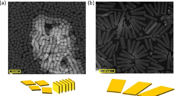
Figure 2.1. A schematic representation of a CdSe nanoplatelet having four CdSe monolayers with an additional Cd layer. ... 10 Figure 2.2. High-angle annular dark-field scanning transmission electron microscopy (HAADF-STEM) images of 4 monolayer thick CdSe nanoplatelets (vertical thickness ~1.2 nm) with different lateral extents: (a) 15 by 15 nm, (b) 35 by 10 nm. ... 11 Figure 2.3. High resolution transmission electron microscopy (TEM) images of (a) 4 monolayer thick CdSe nanoplatelet having a fixed vertical thickness of ~1.2 nm, (b) CdSe-core/CdSe-shell nanoplatelet having a fixed vertical thickness of ~2.7 nm. Green shaded area is drawn as an overlayer to highlight the vertical thickness of the nanoplatelets since they do not perfectly stand upright on the TEM grid. ... 11 Figure 2.4. (a) Colloidal quantum dots having size polydispersity results in inhomogeneous broadening of their emission spectrum in their ensembles. (b) Colloidal nanoplatelets having magic-sized vertical thickness and large lateral sizes (larger than the exciton Bohr radius) do not exhibit inhomogeneous broadening in their ensembles. ... 13 Figure 2.5. Photoluminescence emission spectra of 3, 4 and 5 ML thick CdSe nanoplatelets. 3, 4 and 5 ML CdSe nanoplatelets have their peak emission at 463, 513 and 551 nm, respectively. Full-width at half-maximum of the emission is ~8-10 nm (35 - 40 meV) at room temperature. ... 14 Figure 2.6. (a) Optical absorption spectrum of a 4 ML thick CdSe nanoplatelet in its solution state (dissolved in hexane). (b) Step-like density of states in the nanoplatelets,
xii
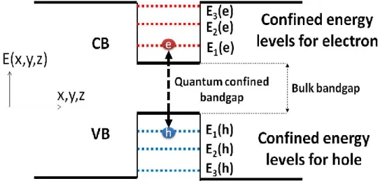
resembling quantum wells, with additional excitonic features arising from the six-fold degenerate valence band of the CdSe (heavy hole, light hole and split-off states). ... 15 Figure 2.7. Heterostructured nanoplatelets: core/crown (lateral extension), core/shell (vertical coating) and core/crown/shell architectures. ... 17 Figure 2.8. Evolution of the quantum confined energy levels for the electron and hole. Quantum confinement leads to a larger effective bandgap than that of the bulk form of the material. ... 20 Figure 2.9. E-k diagram for (a) a bulk semiconductor, (b) a quantum dot without considering exciton effect, and (c) a quantum dot considering exciton effect. ... 22 Figure 2.10. (a) Atomic-like electronic states in a spherical CdSe quantum dot, (b) exciton manifold formed by the first four energy states. (c) Steady state optical absorption spectrum demonstrating the first four allowed transitions. The transitions are not sharp since measurement is made at room temperature Homogenous and inhomogeneous broadening overall broadens these atomic-like transitions. From V. I. Klimov, “Spectral and Dynamical Properties of Multiexcitons in Semiconductor Nanocrystals,” Annual Review of Physical Chemistry 58, 635-673 (2007). ... 23 Figure 2.11. Essential excitonic processes are schematically illustrated: (a) Exciton formation via optical excitation or electrical charge injection, (b) radiative and nonradiative recombination, (c) exciton diffusion, (d) exciton dissociation, and (e) excitation energy transfer (FRET and Dexter energy transfer mechanisms). (HOMO: highest occupied molecular orbital level, LUMO: lowest occupied molecular orbital level, |X1> represents the band edge exciton state, |g> is the ground state.) ... 28
Figure 2.12. Basic optical processes in a two-level atomic system: (a) spontaneous emission, (b) stimulated emission and (c) absorption. ... 33 Figure 2.13. Photon flux entering a medium at z = 0 and the medium length is Δz. The increase of the flux indicates the dominant net optical gain in the system. If flux does not change at all, the medium is in transparency condition (equal amount of absorption and stimulated emission), whereas if flux decreases as light propagates, this indicates the presence of dominant absorption process. ... 37 Figure 2.14. Schematic of a waveguide having a gain material within. The end mirror reflectivities of the waveguide are R1 and R2. There is also intrinsic waveguide loss
xiii
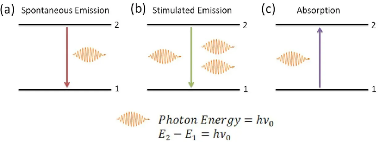
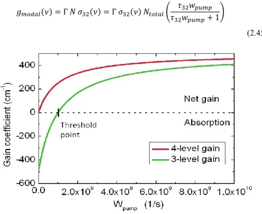
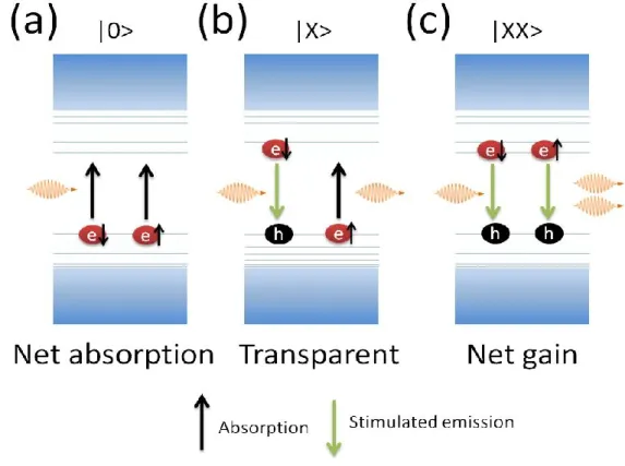
Figure 2.15. Commonly considered gain systems: (a) two-level system, where net gain is not possible, (b) three-level system and (c) four-level system. ... 40 Figure 2.16. Gain coefficients in a four-level and three-level gain systems having the same stimulated emission cross-section, optical confinement factor and spontaneous emission lifetime. Four-level gain system acts as a “thresholdless” laser, whereas three-level gain medium requires a threshold pump rate to achieve net gain. ... 42 Figure 2.17. (a) Calculated gain spectra for GaInAs/InP quantum dot (10 nm 10 nm 10 nm), quantum wire (10 nm 10 nm), quantum well (10 nm) and bulk at room temperature. (b) Calculated maximum gain as a function of the injection current density for the same material system with varying quantum confinement dimensionality. [1986] IEEE reprinted, with permission, from [M. Asada, Y. Miyamoto, Y. Suematsu, Gain and the threshold of three-dimensional quantum-box lasers, IEEE Journal of Quantum Electronics, and Sep/1986.] ... 44 Figure 2.18. Quantum dots in three different states: (a) Ground state (|0>), (b) single exciton state (|X>) and (c) biexciton state (|XX>). (a) ground-state quantum dot has net absorption, while (b) quantum dot in |X> state leads to transparency. (c) |XX> state can provide net gain. ... 45 Figure 2.19. (a) Radiative emission of a biexciton state. (b) Nonradiative Auger recombination of a biexciton state. The recombination energy of the exciton is given to a third particle, i.e., electron or hole, to produce a hot carrier, which then relaxes to band-edge via interacting with phonons (lattice vibrations). Thus, energy is lost into heat. ... 46 Figure 2.20. Optical gain model in conventional colloidal nanocrystals. (a) Exciton manifold for the |0>, |X> and |XX> states and their transitions (black: upward for absorption, red: downward for radiative emission). (b) Electronic picture of the optical gain. |X> is optically transparent. |XX> state can achieve net gain, while |0> has net absorption. NXX should overcome N0 to realize population inversion. ... 47
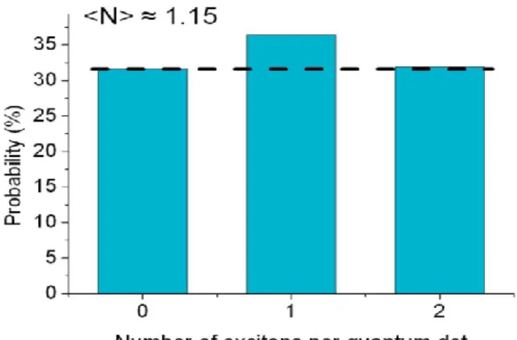
Figure 2.21 Occurrence probabilities of the number of excitons (e.g., 0, 1 and 2) per quantum dot when the average number of excitons is (<N>) 1.15. This excitation level induces the transparency since the population difference N = NXX – N0 ≈ 0. ... 48
xiv
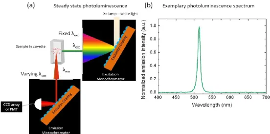
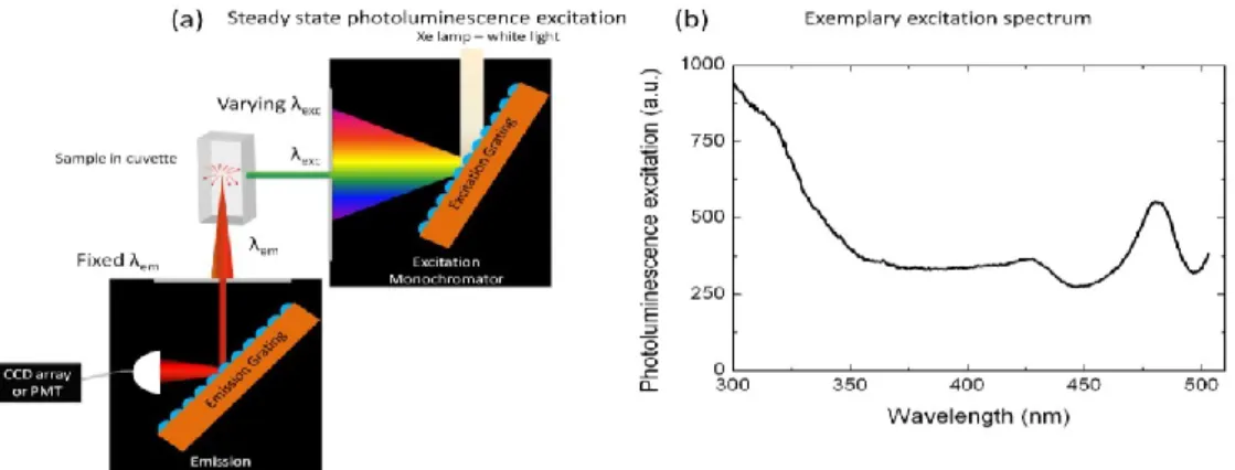
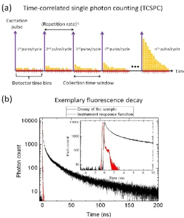
Figure 3.1. (a) Schematic diagram of an experimental setup that can be used to perform steady state linear absorption spectroscopy. (a) An exemplary absorbance data of a four monolayer thick CdSe nanoplatelet in hexane. ... 51 Figure 3.2. (a) Schematic diagram of the experimental setup to measure steady state photoluminescence spectrum. (a) An exemplary photoluminescence spectrum of a four monolayer thick CdSe nanoplatelet in hexane. ... 52 Figure 3.3. (a) Schematic diagram of the experimental setup for steady state photoluminescence excitation spectroscopy. (a) An exemplary excitation spectrum of a four monolayer thick CdSe nanoplatelets in hexane. ... 53 Figure 3.4. (a) Schematic diagram explaining the working principle of time-correlated single photon counting technique for time-resolved fluorescence spectroscopy. (b) Exemplary fluorescence decay curve measured at the peak emission wavelength of a four monolayer CdSe nanoplatelet (black curve) together with the instrument response function (IRF) (red curve). The inset shows the decay curve and the IRF in an early time window. ... 55 Figure 3.5. (a) Schematic diagram of the experimental setup to measure amplified spontaneous emission under single-photon absorption pumping (pump laser 400 nm, 120 fs, 1 kHz repetition rate). (b) Exemplary emission spectra from a four monolayer thick CdSe nanoplatelet film showing the transition from spontaneous emission into amplified spontaneous emission as the pump intensity is gradually increased... 58 Figure 3.6. (a) Schematic diagram of the experimental setup to measure amplified spontaneous emission under two-photon absorption pumping (pump laser 800 nm, 120 fs, 1 kHz repetition rate). (b) Exemplary input-output plot from a four monolayer thick CdSe nanoplatelet film showing the transition from spontaneous emission into amplified spontaneous emission as a function of the pump intensity. The threshold for optical gain can be also characterized from this plot. ... 58 Figure 3.7. Solid film of a colloidal nanoplatelet (heterostructured CdSe/CdTe core/crown architecture) film encapsulated with a cover glass and epoxy. The sample is excited in stripe geometry with a femtosecond laser. Emission from the sample (a) below and (b) above the amplified spontaneous emission threshold. ... 59
xv
Figure 3.8. CdSe/CdS core/shell quantum dots spin-coated on quartz substrate excited with a pump intensity above the amplified spontaneous emission threshold. ... 60 Figure 3.9. (a) Schematic diagram of the experimental setup to perform variable stripe length (VSL) method for the measurement of net modal gain coefficients. (b) Exemplary data for the variable stripe length measurement. ... 61 Figure 3.10. (a) Schematic diagram of the experimental setup for open aperture z-scan technique. (b) Exemplary transmittance data for a four monolayer CdSe nanoplatelet in toluene as the sample is translated through the focus of 800 nm femtosecond Gaussian laser beam. ... 63 Figure 3.11. Open aperture z-scan setup to measure the nonlinear absorption cross-section constructed and used for this thesis work. ... 63 Figure 4.1. (a) Absorbance (dashed line) and photoluminescence (solid line) spectrum, (b) transmission electron microscopy images of the 4 ML CdSe NPLs. Reprinted (or Adapted) with permission from [19]. Copyright 2014 American Chemical Society.... 72 Figure 4.2. TEM images of the highly stacked NPLs. The scale bar is (a) 400 nm and (b) 100 nm. Column-like ordered stacking of the NPLs is clearly visible. Reprinted (or Adapted) with permission from [19]. Copyright 2014 American Chemical Society.... 73 Figure 4.3. High-angle annular dark-field (HAADF) TEM images of the NPLs with (a) no ethanol, a total of (b) 55 µL, (c) 135 µL, and (d) 455 µL ethanol added. The scale bars are 100 nm. As the total added ethanol amount is increased gradually, longer column-like stacks of the NPLs are formed. On each image, cartoon like depiction of the evolution of the stacking in NPLs is presented by yellow-colored NPLs. Reprinted (or Adapted) with permission from [19]. Copyright 2014 American Chemical Society. ... 74 Figure 4.4. (a) Time resolved photoluminescence decays together with their multi-exponential fits. Inset shows the same photoluminescence decay curves in a shorter time window. (b) Steady state photoluminescence intensity of the NPLs while ethanol is added gradually to the solution of the NPLs. Inset shows the peak emission wavelength and photoluminescence FWHM of the NPLs as a function of the total added amount of ethanol. (c) Amplitude averaged photoluminescence lifetimes of the NPLs shown by black dots as a function of the total added ethanol amount. Blue stars
xvi
show the modeled photoluminescence lifetimes of the NPLs for 0, 55, 135 and 455 µL ethanol added cases. The inset shows the average photoluminescence lifetimes of the NPLs in PBMA host matrix given for different NPL/PBMA volume ratios. Transition from non-stacking to stacking in the photoluminescence decay kinetics of the NPLs is observed without using any ethanol. As the NPL/PBMA volume ratio is gradually increased, phase segregation occurs that result in stacking. This increases the total decay rate of the NPLs. (d) Photoluminescence QY of the NPLs as a function of total added ethanol amount measured directly from steady state photoluminescence measurements and calculated semi-empirically from the photoluminescence lifetimes assuming the radiative recombination does not change. Reprinted (or Adapted) with permission from [19]. Copyright 2014 American Chemical Society. ... 75 Figure 4.5. Amplitude averaged photoluminescence lifetime of the NPLs as a function of wavelength measured for (a) 0 µL, (b) 50 µL and (c) 455 µL ethanol addition. Reprinted (or Adapted) with permission from [19]. Copyright 2014 American Chemical Society. ... 77 Figure 4.6. Photoluminescence lifetime components (a) τ1, (b) τ2, (c) τ3 and (d) τ4,
along with their contribution to the overall emission (a) A1τ1, (b) A2τ2, (c) A3τ3 and (d)
A4τ4, respectively. Reprinted (or Adapted) with permission from [19]. Copyright 2014
American Chemical Society. ... 78 Figure 4.7. Photoluminescence decays of the NPLs in PBMA polymer host matrix in drop-casted solid thin film samples having different NPL/PBMA volume ratio. In the case of the smallest NPL/PBMA volume ratio, NPLs are well-separated in the polymer matrix as observed by their slower photoluminescence decay kinetics. As the NPL/PBMA volume ratio is increased, the photoluminescence decays become faster due to stacking of the NPLs via phase segregation in the polymer matrix. Reprinted (or Adapted) with permission from [19]. Copyright 2014 American Chemical Society.... 80 Figure 4.8. Schematic depicting the ultra-long range exciton transfer in the stacked NPL assemblies via exciton hopping through homo-FRET. The non-emissive NPL in the stack causes trapping with the assistance of long-range exciton migration causing nonradiative recombination of the excitons that quenches the photoluminescence emission of the NPLs in the stack. Reprinted (or Adapted) with permission from [19]. Copyright 2014 American Chemical Society. ... 83
xvii
Figure 4.9. a) A sample NPL stack with 20 NPLs. The shaded spots schematically represent the defected NPLs. b) Exciton dynamics acting on the NPL located in the ith
index of a stack array. The recombination and other energy transfer processes related to (i-1)th and (i+1)th NPLs are not shown. Reprinted (or Adapted) with permission from
[19]. Copyright 2014 American Chemical Society. ... 84 Figure 4.10. Distribution of stack size for the nanoplatelet solution mixed with a) 55 µL, b) 135 µL and c) 455 µL ethanol. Reprinted (or Adapted) with permission from [19]. Copyright 2014 American Chemical Society. ... 84 Figure 4.11. Absorption (dashed lines ) and photoluminescence (solid lines) of the 4 ML (cyan) and 5 ML (red) NPLs. Reprinted with permission from The Royal Society of Chemistry [68]. Copyright 2015 The Royal Society of Chemistry. ... 94 Figure 4.12. HAADF-TEM images of the NPLs of (a) 4 ML having the average size of 23.57 nm (± 2.90 nm) by 12.17 nm (± 1.94 nm) and (b) 5 ML having the average size of 26.32 nm (± 2.55 nm) by 9.04 nm (± 1.41 nm). Stacking of the NPLs is clearly visible in both NPL populations. The scale bars are 100 nm. Reprinted with permission from The Royal Society of Chemistry [68]. Copyright 2015 The Royal Society of Chemistry. ... 95 Figure 4.13. Confocal images of the mixed solid films of the 4 and 5 ML NPLs. The collection window is (a) 505-530 nm matching only the emission of 4 ML NPLs, (b) 560-615 nm matching only with the emission of 5 ML NPLs. In both images, artificial coloring is used to represent the emission intensity. The scale bar is 100 µm. Reprinted with permission from The Royal Society of Chemistry [68]. Copyright 2015 The Royal Society of Chemistry... 96 Figure 4.14. Time resolved fluorescence spectroscopy of the (a) 4 ML and (b) 5 ML NPLs in their solid thin films. Reprinted with permission from The Royal Society of Chemistry [68]. Copyright 2015 The Royal Society of Chemistry. ... 97 Figure 4.15. (a) Photoluminescence excitation spectra of the 4 and 5 ML NPLs featuring the electron/light-hole and continuum bands. (b) Enhancement of the 5 ML NPL PLE owing to the NRET from the 4 ML NPLs. Reprinted with permission from The Royal Society of Chemistry [68]. Copyright 2015 The Royal Society of Chemistry. ... 100
xviii
Figure 4.16. Enhancement of the acceptor NPL emission excitation exhibiting spectral features resembling the spectral PLE features of the donor NPLs. At small A:D ratios, the dominant excitation mechanism of the acceptor NPLs is through NRET, whereas at large A:D ratios the acceptor NPLs are dominantly excited through direct absorption of the pump photons. Reprinted with permission from The Royal Society of Chemistry [68]. Copyright 2015 The Royal Society of Chemistry. ... 102 Figure 4.17. NRET efficiency as a function of A:D ratio. Reprinted with permission from The Royal Society of Chemistry [68]. Copyright 2015 The Royal Society of Chemistry. ... 104 Figure 4.18. HAADF-TEM images of mixed NPL populations incorporating 2-3% 4 ML NPLs while the rest of the NPLs are 5 ML. 4 ML NPLs have the square-like shape with an average size of 10.81 nm (± 0.53 nm) and 5 ML NPLs have the rectangle-like shape with an average size of 43.67 nm (± 3.31 nm) and 12.94 nm (± 1.51 nm). Reprinted with permission from The Royal Society of Chemistry [68]. Copyright 2015 The Royal Society of Chemistry. ... 105 Figure 4.19. HAADF-TEM image of the mixed NPL assembly (without size selective precipitation) of square-like 4 ML NPLs and rectangle-like 5 ML NPLs. Schematic of the NRET as limited by the nanoscale phase segregation between the NPLs of different populations. Reprinted with permission from The Royal Society of Chemistry [68]. Copyright 2015 The Royal Society of Chemistry. ... 106 Figure 4.20. General reaction scheme for the incorporation of anchor groups into the block copolymer containing a conjugated DEH-PPV block and assignment of the polymers P1 and P2a-c. Reprinted (or Adapted) with permission from [185]. Copyright 2014 American Chemical Society. ... 112 Figure 4.21. (a) FTIR spectra verifying the success of the post-polymerization modification and (b) 19F-NMR spectra of polymers P1 and P2a. While the signals of
the reactive ester occur in the 19F-NMR spectrum of precursor polymer P1, full
conversion of the post-polymerization modification is evidenced by the absence of any signals in the spectrum of polymer P2a. Reprinted (or Adapted) with permission from [185]. Copyright 2014 American Chemical Society. ... 114 Figure 4.22. (a) FTIR spectra verifying the success of the post-polymerization modification and (b) 19F-NMR spectra of polymers P1 and P2b. While signals of the
xix
reactive ester occur in the 19F-NMR spectrum of precursor polymer P1, full conversion
of the post-polymerization modification is evidenced by the absence of any signals in the spectrum of polymer P2b. Reprinted (or Adapted) with permission from [185]. Copyright 2014 American Chemical Society. ... 114 Figure 4.23. (a) FTIR spectra verifying the successful post-polymerization modification (transferring P1 to P2c) and (b) 19F-NMR spectra of polymers P1 and
P2c. While signals of the reactive ester occur in the 19F-NMR spectrum of precursor
polymer P1, no signals occur in the spectrum of P2c which verify full conversion of the post-polymerization modification. Reprinted (or Adapted) with permission from [185]. Copyright 2014 American Chemical Society. ... 115 Figure 4.24. 400 MHz 1H-NMR spectra of the precursor polymer P1 and polymer P2a
carrying a sulfide anchor group (in CDCl3). After post-polymerization modification
signals of the anchor group are detected in the spectrum. Reprinted (or Adapted) with permission from [185]. Copyright 2014 American Chemical Society. ... 115 Figure 4.25. 400 MHz 1H-NMR spectra of the precursor polymer P1 and polymer P2b
carrying an amino anchor group (in CDCl3). After post-polymerization modification
signals of the anchor group are detected in the spectrum. Reprinted (or Adapted) with permission from [185]. Copyright 2014 American Chemical Society. ... 116 Figure 4.26. 400 MHz 1H-NMR spectra of the precursor polymer P1 and polymer P2c
carrying an amino anchor group (in CDCl3). After post-polymerization modification
signals of the anchor group are detected in the spectrum. Reprinted (or Adapted) with permission from [185]. Copyright 2014 American Chemical Society. ... 117 Figure 4.27. Absorbance (solid) and photoluminescence (dotted) of (a) 4 monolayer thick CdSe nanoplatelets, and (b) conjugated polymers P1 and P2a-c. Inset in (a) shows the HAADF-STEM image of the CdSe nanoplatelets, the scale bar is 50 nm. Reprinted (or Adapted) with permission from [185]. Copyright 2014 American Chemical Society. ... 118 Figure 4.28. Steady-state photoluminescence spectra of the hybrids as the polymer were added step by step in the case of (a) NPL-P2a, (b) NPL-P2b and (c) NPL-P1 samples. The excitation wavelength for all cases was 375 nm. The insets in (a) and (b) show the NPL emission after spectral shape of the polymer emission has been subtracted. (d) Evolution of the NPL emission as a function of the added polymer
xx
amount for three different cases. Reprinted (or Adapted) with permission from [185]. Copyright 2014 American Chemical Society. ... 121 Figure 4.29. (a) Emission of the only polymer P2a and NPL + P2a for 5.2 nmol (top) and 2.6 nmol (bottom) polymer amounts. The excitation wavelength for all cases is 375 nm. (b) Emission intensity change in the polymers P2a and P2b in the presence of the NPLs as compared to bare polymer emission. Reprinted (or Adapted) with permission from [185]. Copyright 2014 American Chemical Society. ... 122 Figure 4.30. (a) Excitation spectra of the NPL emission for three different samples: only NPL (green), NPL + 1.4 nmol P2a (dark blue) and NPL + 2.8 nmol P2a (light blue). Excitation of the NPL emission is estimated by considering absorption of the excitation light by the P2a for two different cases (dotted curves). (b) Excitation spectra of the P2a for only 5.6 nmol P2a (red dotted curve) and NPL + 5.6 nmol P2a (red solid curve) samples. Also, excitation of the P2a emission is estimated by considering absorption of the excitation light by the NPLs (black solid curve). (c) Excitation spectra of the P1 for only 5.2 nmol P1 (orange dotted curve) and NPL + 5.2 nmol P1 (orange solid curve) samples. Also, excitation of the P1 emission is estimated by considering absorption of the excitation light by the NPLs (black solid curve). (d) Energy bands of the NPLs and polymers exhibiting a staggered (Type II) band alignment favoring exciton dissociation. Reprinted (or Adapted) with permission from [185]. Copyright 2014 American Chemical Society. ... 125 Figure 4.31. (a) Quenching of the NPL’s excitation spectra in the NPL+1.4 nmol P2a and NPL+2.8 nmol P2a samples with respect to NPL-only sample. (b) Quenching of the P2a’s excitation spectra in the NPL+5.6 nmol P2a sample with respect to P2a-only sample. Reprinted (or Adapted) with permission from [185]. Copyright 2014 American Chemical Society. ... 126 Figure 4.32. Cyclic voltammetry measurement of precursor polymer P1 measured in a 0.1 M solution of TBAPF6 in anhydrous acetonitrile versus Fc/Fc+. Reprinted (or Adapted) with permission from [185]. Copyright 2014 American Chemical Society. ... 127 Figure 4.33. Emission spectra of the only NPL, NPL + 9 nmol P2b and NPL + 9 nmol P2c samples. The inset shows the NPL emission after spectral profile of the polymer emission is subtracted. The emission quenching is larger for P2b than P2c since P2b
xxi
has a shorter anchor ligand. Reprinted (or Adapted) with permission from [185]. Copyright 2014 American Chemical Society. ... 129 Figure 4.34. HAADF-STEM images of (a) only NPLs and (b) NPL-P2a hybrids. The insets show zoomed-in images with scale bar of 100 nm. Reprinted (or Adapted) with permission from [185]. Copyright 2014 American Chemical Society. ... 130 Figure 4.35. Absorption and photoluminescence spectra of (a) the blue-emitting CdZnS/ZnS core/shell QDs and (b) the green-emitting 4ML CdSe NPLs, which are dissolved in hexane at room temperature. High-angle annular dark-field scanning transmission electron microscopy (HAADF-STEM) images of (c) the donor-QDs having 9.3 ± 1.2 nm and (d) the acceptor-NPLs having 12.8 ± 1.9 nm by 10.5 ± 1.5 nm mean sizes. The inset in (c) shows the transmission electron microscopy (TEM) image of a CdZnS/ZnS core/shell QDs. Reprinted by permission from Wiley [110], Copyright 2015 Wiley-VCH Verlag GmbH & Co. KGaA, Weinheim... 137 Figure 4.36. Scanning electron microscopy (SEM) images of the hybrid solid thin films of the donor QDs (bright ones) and the acceptor NPLs having 0.01 D/A molar ratio for (a) 500 nm and (b) 100 nm scale bars. The yellow and blue arrows given in (b) point at the QDs and the NPLs, respectively. Reprinted by permission from Wiley [110], Copyright 2015 Wiley-VCH Verlag GmbH & Co. KGaA, Weinheim. ... 138 Figure 4.37. Steady-state PL spectra of the solid films of donor (blue line), only-acceptor (green line) and donor-only-acceptor having D/A= 0.10 (red line) cases. Reprinted by permission from Wiley [110], Copyright 2015 Wiley-VCH Verlag GmbH & Co. KGaA, Weinheim. ... 139 Figure 4.38. Time-resolved fluorescence decay curves of the solid thin film samples including donor-only, acceptor-only and hybrid cases with varying D/A molar ratios measured (a) at the donor band-edge emission wavelength (453 nm) and (b) at the acceptor band-edge emission wavelength (513 nm). The insets show the zoom-in of the same decay curves and the impulse response function (IRF). Reprinted by permission from Wiley [110], Copyright 2015 Wiley-VCH Verlag GmbH & Co. KGaA, Weinheim. ... 141 Figure 4.39. Evolution of the nonradiative energy transfer (NRET) efficiency as a function of the donor QDs to acceptor NPLs (D/A) molar ratios. The dash-dot lines are
xxii
a guide for the eyes. Reprinted by permission from Wiley [110], Copyright 2015 Wiley-VCH Verlag GmbH & Co. KGaA, Weinheim. ... 145 Figure 4.40. (a) Photoluminescence excitation (PLE) spectra of the only-donor QDs (blue-line) and the only-acceptor NPLs (green-line) measured at their emission peak wavelengths (453 and 513 nm, respectively). (b) Excitation spectra of the samples having different D/A ratio normalized at the e-lh transition peak wavelength (480 nm). The inset shows the enhancement in the excitation spectra of the hybrid donor-acceptor samples due to the NRET from donor QDs. Reprinted by permission from Wiley [110], Copyright 2015 Wiley-VCH Verlag GmbH & Co. KGaA, Weinheim. ... 147 Figure 4.41. Time-resolved fluorescence decay curves of the solid thin film samples including (a) the donor-only, (b) the acceptor-only, and the blended case of donor and acceptor for D/A=0.01 molar ratio measured (c) at the donor band-edge emission wavelength (453 nm) and (d) at the acceptor band-edge emission wavelength (513 nm). The dashed arrows show the direction of decreasing temperature. The insets show the zoom-in for the early phase, along with the impulse response function (IRF). Reprinted by permission from Wiley [110], Copyright 2015 Wiley-VCH Verlag GmbH & Co. KGaA, Weinheim. ... 148 Figure 4.42. (a) Evolution of the NRET efficiency (ηNRET) for D/A=0.01 ratio as a
function of the temperature. The dash-dot lines show the linear fitting curve with 0.032 of slope. (b) Enhancement in ηNRET corresponding based on the experimental data
(blue-circle) and the calculated results using the shift in spectral overlap between the PL spectrum of donor and the absorption spectrum of acceptor (black-diamond) and those using both the shift in spectral overlap and the change in PL QY with decreasing temperature. Reprinted by permission from Wiley [110], Copyright 2015 Wiley-VCH Verlag GmbH & Co. KGaA, Weinheim. ... 150 Figure 4.43. (a) Temperature dependent 1-T (transmission) spectra for the acceptor-only case. (b) Photoluminescence (PL) spectra of the donor-acceptor-only case at different temperatures. ... 151 Figure 5.1. (a) Representative schematic of the organic-inorganic exciton transferring thin film. (b) Fluorescence of TCTA (violet), FIrpic (cyan) and QDs (red) along with
xxiii
the absorbance of QDs (red-dashed). Reprinted (or Adapted) with permission from [190]. Copyright 2014 American Chemical Society. ... 164 Figure 5.2. Steady state fluorescence spectra of only QDs (red), only TCTA (violet), FIrpic:TCTA (cyan), TCTA/QDs (orange) and FIrpic:TCTA /QDs (green). The organic layer thickness is 20 nm. Reprinted (or Adapted) with permission from [190]. Copyright 2014 American Chemical Society. ... 165 Figure 5.3. (a) PLE at the QD emission peak for the samples of only QDs (red), TCTA/QDs (orange), FIrpic:TCTA/QDs (green) when the organic film thickness is 20 nm. (b) Normalized PLE spectrum of FIrpic emission (cyan) from the FIrpic:TCTA sample and PLE spectrum of TCTA emission from the bare TCTA sample. (c) Cascaded exciton transfer from the organic layer into the QDs (TCTAFIrpicQDs). Reprinted (or Adapted) with permission from [190]. Copyright 2014 American Chemical Society. ... 166 Figure 5.4. (a) Phosphorescence decay curves and their fits for the FIrpic emission from the samples of FIrpic:TCTA (cyan) and FIrpic:TCTA/QDs (red) when the organic film thickness is 20 nm. (b) Fluorescence decay curves and fits for the QD emission from the samples of only QDs (red), TCTA/QDs (orange) and FIrpic:TCTA/QDs (green). The inset exhibits the decay in an early time frame. All of the time resolved measurements were performed using a pulsed laser at 375 nm. Reprinted (or Adapted) with permission from [190]. Copyright 2014 American Chemical Society. ... 169 Figure 5.5. (a) Fluorescence enhancement factors of the QD emission in the samples of TCTA/QDs (orange) and FIrpic:TCTA/QDs (green) as a function of the organic film thickness and the modelled enhancement factors plotted in dashed curves. (b) Modelled NRET efficiency in the TCTA:FIrpic/QDs sample as a function of organic layer thickness with and without exciton diffusion assistance together with experimentally measured NRET efficiency from time resolved fluorescence measurements. Reprinted (or Adapted) with permission from [190]. Copyright 2014 American Chemical Society. ... 172 Figure 5.6. Photoluminescence of the QD/FIrpic:TCTA samples when excited at 330 nm. Reprinted (or Adapted) with permission from [190]. Copyright 2014 American Chemical Society. ... 174
xxiv
Figure 5.7. (a) 3D schematic of the QLED designed to achieve efficient energy transfer pumping. (b) Energy band alignment of the device in the structure of ITO/PEDOT:PSS/poly-TPD/QD/BPhen/Ir(ppy)3TCTA/TPBI/LiF/Al. Reprinted (or
Adapted) with permission from [21]. Copyright 2014 American Chemical Society.. 178 Figure 5.8. (a) Normalized electroluminescence spectra of the ITO/PEDOT:PSS/poly-TPD/QD/TPBI/LiF/Al, ITO/PEDOT:PSS/poly-TPD/QD/TCTA:Ir(ppy)3/TPBI/LiF/Al.
(b) Normalized electroluminescence spectra of ITO/PEDOT:PSS/poly-TPD/QD/BPhen/TCTA:Ir(ppy)3/TPBI/LiF/Al with varying the BPhen thickness.
Reprinted (or Adapted) with permission from [21]. Copyright 2014 American Chemical Society. ... 179 Figure 5.9. The current-voltage profile of the devices:
ITO/PEDOT:PSS/poly-TPD/QD/ TCTA:Ir(ppy)3/TPBI/LiF/Al and
ITO/PEDOT:PSS/poly-TPD/QD/BPhen/TCTA:Ir(ppy)3/TPBI/LiF/Al. Reprinted (or Adapted) with permission
from [21]. Copyright 2014 American Chemical Society. ... 180 Figure 5.10. Schematic of the partially phosphorescent co-doped electron transport layer of TCTA. The partial co-doping is positioned in four different zones within the TCTA as indicated by positions 1 to 4 above the scheme, where position 1 is the closest to the QDs. NRET is expected to be the strongest for the co-doping located at the position 1. Reprinted (or Adapted) with permission from [21]. Copyright 2014 American Chemical Society. ... 182 Figure 5.11. (a) Non-normalized electroluminescence spectra of the ITO/PEDOT:PSS/poly-TPD/QD/BPhen/TCTA:Ir(ppy)3/TPBI/LiF/Al device with
varying the position of the co-doped TCTA:Ir(ppy)3 layer within the TCTA electron
transport layer. (b) External quantum efficiencies of the devices at 5 mA injection current as a function of the position of the co-doping layer into TCTA. (c) EQE vs. current density of the devices: energy transfer pumping and color purity optimized ITO/PEDOT:PSS/poly-TPD/QD/BPhen(1.5 nm)/TCTA:Ir(ppy)3(2.5nm)/TCTA
(7.5nm)/TPBI/LiF/Al and conventional ITO/PEDOT:PSS/poly-TPD/QD/TPBI/LiF/Al. (d) Electroluminescence spectra of the outperforming ITO/PEDOT:PSS/poly-TPD/QD/BPhen/TCTA:Ir(ppy)3/TPBI/LiF/Al device (Ir(ppy)3 doping in the first 2.5
nm of the TCTA layer). Reprinted (or Adapted) with permission from [21]. Copyright 2014 American Chemical Society. ... 183
xxv
Figure 5.12. The luminance - current profile of the optimized device of ITO/PEDOT:PSS/poly-TPD/QD/BPhen/TCTA:Ir(ppy)3/TPBI/LiF/Al. (2.5 nm
codoped layer is just positioned next to the BPhen layer). Reprinted (or Adapted) with permission from [21]. Copyright 2014 American Chemical Society. ... 184 Figure 5.13. Time resolved fluorescence spectra of the quantum dot (QD) layer in the bare and in various architecture samples (QD/BPhen, QD/TCTA, QD/Ir(ppy)3:TCTA,
QD/ BPhen /Ir(ppy)3:TCTA) along with the bi-exponential fits given with white dots.
Reprinted (or Adapted) with permission from [21]. Copyright 2014 American Chemical Society. ... 186 Figure 6.1 Structure of the core/shell ZnCdS/ZnS quantum dots that simultaneously combine large size, high stability and suppressed Auger recombination thanks to the gradient core/shell interface. ... 195 Figure 6.2 (a) Absorbance and (b) photoluminescence of the blue-emitting CdZnS/ZnS QDs having different shell growth time. (c) Transmission electron microscopy images of the different shell grown QDs. Reprinted (or Adapted) with permission from [274]. Copyright 2014 American Chemical Society. ... 196 Figure 6.3 Zn/Cd ratio of the graded QDs with shells grown in 30, 120, and 180 min measured with XPS as a function of etching time. Linear fits are presented to guide the eye. Reprinted (or Adapted) with permission from [274]. Copyright 2014 American Chemical Society ... 197 Figure 6.4 Pump intensity dependent PL of (a) 30 min, (b) 120 min and (c) 180 min shell grown CdZnS/ZnS QDs under 1PA pumping. (d) Luminescence vs. pump intensity curve of the 180 min shell grown QDs with 1PA pumping. Reprinted (or Adapted) with permission from [274]. Copyright 2014 American Chemical Society. ... 199 Figure 6.5 Pump intensity dependent PL of (a) 30 min, (b) 120 min and (c) 180 min shell grown CdZnS/ZnS QDs under 2PA pumping. (d) Luminescence vs. pump intensity curve of the 30 min, 120 min and 180 min shell grown QDs with 2PA pumping. Reprinted (or Adapted) with permission from [274]. Copyright 2014 American Chemical Society. ... 200
xxvi
Figure 6.6 (a) PL intensity of the 30 min shell grown QDs under 1PA pumping as a function of pump intensity. At higher pump intensities higher-order multiexcitonic ASE is observed in addiation to the regular ASE. (b) Variable striple length measurement of the gain coefficient of the 180 min shell grown QDs pumped by 1PA. Reprinted (or Adapted) with permission from [274]. Copyright 2014 American Chemical Society. ... 202 Figure 6.7 (a) Transmission electron microscopy image of the CdSe/CdS QDs having CdSe core of 2.2 nm radius and 6 monolayer CdS shell. Inset shows the high resolution TEM image of a CdSe/CdS QD with diameter of ~8 nm. (b) XRD patterns of CdSe core (bottom) and CdSe/CdS QDs (top). The CdSe core shows zinc-blende structure with matched XRD pattern to its bulk counterpart. After CdS shell growth, diffraction peaks are shifted to higher angles and become narrower, indicating the increased crystalline quality and alloying at the core/shell interface. (c) Photoluminescence (red, solid) and absorbance (blue, dotted) spectrum of the core/shell QD. Emission line width is less than 30 nm (full width at half maximum – FWHM) suggesting the small size distribution. Reprinted by permission from Wiley [18], Copyright 2015 Wiley-VCH Verlag GmbH & Co. KGaA, Weinheim. ... 208 Figure 6.8 Transient PL intensity measured at the peak emission wavelength at three different excitation levels for (a) CdSe-core/CdS-shell and (b) core-only CdSe QDs. τXX is the multi-exciton lifetime, τX is the single exciton lifetime of the QDs. The
average number of excitons per QD (<N>) was calculated from the excitation levels. (b) Inset shows the decay of the CdSe QDs at an early time window. Reprinted by permission from Wiley [18], Copyright 2015 Wiley-VCH Verlag GmbH & Co. KGaA, Weinheim. ... 210 Figure 6.9 (a) Etch depth profile analysis of the atomic ratio of S to Se. (b) Initial etched part (i.e., top QDs) and deeper etched part (i.e., ensemble region). Reprinted by permission from Wiley [18], Copyright 2015 Wiley-VCH Verlag GmbH & Co. KGaA, Weinheim. ... 213 Figure 6.10 Alloyed vs. abrupt core/shell interface in CdSe/CdS QDs along with their atomic composition throughout the QD. Reprinted by permission from Wiley [18], Copyright 2015 Wiley-VCH Verlag GmbH & Co. KGaA, Weinheim. ... 215
xxvii
Figure 6.11 (a) The emission spectra of the core/shell QD film under 1PA stripe excitation pumping. The inset shows the integrated emission intensity as a function of 1PA pumping energy intensity. (b) 2PA pumped emission spectra of the QDs at various pump intensities. Inset shows the integrated intensity of the emission as a function of 2PA pump intensity. The narrow ASE peak with a FWHM of 5 nm kicks off at the red-tail of the spontaneous emission spectrum (FWHM of ~29 nm). (c) Laser shot dependent ASE intensity under pump laser shots up to 1.8 × 10⁷ indicating the
exceptional stability of the QDs. Reprinted by permission from Wiley [18], Copyright 2015 Wiley-VCH Verlag GmbH & Co. KGaA, Weinheim... 219 Figure 6.12 Variable stripe length technique based measurement of the net modal gain coefficient and the fit to the experimental data. Reprinted by permission from Wiley [18], Copyright 2015 Wiley-VCH Verlag GmbH & Co. KGaA, Weinheim. ... 220 Figure 6.13 Open aperture z-scan measurement reveals the 2PA cross-section of the QDs as 41,885 GM. Although this is not the highest reported 2PA cross-section for the QDs, the threshold for amplified spontaneous emission is the lowest among 2PA pumped QD gain media. This is only possible by the high gain performance of QD materials. Reprinted by permission from Wiley [18], Copyright 2015 Wiley-VCH Verlag GmbH & Co. KGaA, Weinheim. ... 220 Figure 6.14 Optical constants of SiO2 and TiO2 nanoparticle films and absorption of
TiO2 nanoparticles. Reprinted by permission from Wiley [18], Copyright 2016
Wiley-VCH Verlag GmbH & Co. KGaA, Weinheim. ... 221 Figure 6.15 (a) Scanning electron microscopy cross-sectional image of the all-colloidal DBR shows alternating stacks as the results of different spin-casted nanoparticles (SiO2
and TiO2). Focused ion beam was used to create cross section of the colloidal DBR.
Inset shows the close-up of the layered stacks of TiO2 and SiO2 nanoparticles at the
cleaved edge of a DBR. (b) Surface normal reflectance of the DBR stack with 10-bilayer of TiO2 and SiO2 nanoparticles along with the PL of the QDs in the cavity
having optical thickness of about 15 µm. (c) Emission intensity as a function of pump intensity for frequency up-converted all-colloidal VCSEL clearly shows the threshold behavior of the AC-VCSEL. Inset shows the emission spectrum of the laser under different excitation pump density. Single mode lasing is achieved with a Q-factor greater than 430. Lasing peak is narrower than 1.5 nm (limited by the spectral
xxviii
resolution of our measurement system). (d) Photographic image of the lasing spot from the all-colloidal VCSEL. The spectrally and spatially coherent lasing beam is visible as a bright spot on the screen. Reprinted by permission from Wiley [18], Copyright 2015 Wiley-VCH Verlag GmbH & Co. KGaA, Weinheim. ... 222 Figure 6.16 Single- and multi-mode lasing in AC-VCSELs. Depending on the location of the pump spot on the AC-VCSEL, either single-mode or multi-mode lasing is observed when the pump intensity is above the threshold. Reprinted by permission from Wiley [18], Copyright 2015 Wiley-VCH Verlag GmbH & Co. KGaA, Weinheim. ... 224 Figure 6.17 High-angle annular dark-field transmission electron microscopy (HAADF-TEM) images of (a) the core-only and core/crown NPLs having a size of (b) 21, (c) 25 and 32 nm. Reprinted (or Adapted) with permission from [17]. Copyright 2014 American Chemical Society. ... 230 Figure 6.18 Absorbance and photoluminescence of the NPLs: core-only (orange), core/crown NPL having size of 21 nm (blue), 25 nm (green) and 32 nm (red). (b) Photoluminescence excitation spectra of the core-only and core/crown NPLs. Reprinted (or Adapted) with permission from [17]. Copyright 2014 American Chemical Society. ... 231 Figure 6.19 (a) 2PA pumped ASE of the 21 nm size core/crown NPLs. (b) 2PA pumped luminescence vs. pump intensity of the core-only and core/crown NPLs having a size of 21, 25 and 32 nm. Reprinted (or Adapted) with permission from [17]. Copyright 2014 American Chemical Society. ... 233 Figure 6.20 2PA pumped ASE of the core-only and core/crown NPLs having size of 25 and 32 nm. Reprinted (or Adapted) with permission from [17]. Copyright 2014 American Chemical Society. ... 233 Figure 6.21 (a) 1PA pumped ASE of the 21 nm size core/crown NPLs. (b) 1PA pumped luminescence vs. pump intensity of the core-only and core/crown NPLs having a size of 21, 25 and 32 nm. (c) Variable stripe length measurement of the gain coefficient. Reprinted (or Adapted) with permission from [17]. Copyright 2014 American Chemical Society. ... 235
xxix
Figure 6.22 1PA pumped ASE of the core-only and core/crown NPLs having size of 25 and 32 nm. Reprinted (or Adapted) with permission from [17]. Copyright 2014 American Chemical Society. ... 235 Figure 6.23 (a) Schematic of the VCSEL of the NPLs that employ DBRs having 6-bilayers stack of SiO2 and TiO2 nanoparticles each. (b) Emission spectrum of the
VCSEL is plotted as the pump intensity is progressively increased. (c) Integrated emission intensity vs. pump intensity measurement and the linear fits indicating the 2PA pumped lasing threshold of 2.49 mJ/cm2. Reprinted (or Adapted) with permission from [17]. Copyright 2014 American Chemical Society. ... 236 Figure 6.24 Transmission electron microscopy (TEM) images of the 4 ML CdSe NPLs having different lateral sizes: (a) 170.0 ± 22.5 nm2 (NPL-1), (b) 269.6 ± 38.6 nm2
(NPL-2), (c) 377.6 ± 56.4 nm2 (NPL-3) and (d) 391.9 ± 65.7 nm2 (NPL-4), grown
using different growth times. Reprinted (or Adapted) with permission from [66]. Copyright 2015 American Chemical Society. ... 241 Figure 6.25 Absorption and photoluminescence spectra of the 4ML CdSe NPLs grown in lateral direction with different growth times. The peaks labeled as e-lh and e-hh in the absorption spectrum correspond to the electron-light hole and the electron-heavy hole transitions, respectively. Reprinted (or Adapted) with permission from [66]. Copyright 2015 American Chemical Society. ... 242 Figure 6.26 (a) Time-resolved fluorescence decays of the NPLs having different lateral sizes. The inset shows the zoom-in of the same TRF decay. Evolution of (b) the lifetime components of fluorescence decays, (c) the amplitude-averaged photoluminescence lifetimes, (d) photoluminescence quantum efficiency (PL-QE) (e) the percentage steady state contribution from each decay component of the NPLs and (f) calculated fraction of NPL sub-populations as a function of the lateral size. The dotted lines are a guide for eyes. Reprinted (or Adapted) with permission from [66]. Copyright 2015 American Chemical Society. ... 245 Figure 6.27 Photoluminescence quantum efficiency (PL-QE) measurements of the 4ML CdSe NPLs grown in lateral direction using different growth times, in comparison to the reference dye of Rhodamine 6G (Rh6G) with 95% PL-QE. Reprinted (or Adapted) with permission from [66]. Copyright 2015 American Chemical Society. ... 247
xxx
Figure 6.28 The schematic representation of the non-defected (yellow) and defected (red) NPLs within the NPL ensembles. The relative change of the fraction of these two different NPL populations as a function of lateral area is shown to match the experimental PL QEs. Reprinted (or Adapted) with permission from [66]. Copyright 2015 American Chemical Society. ... 250 Figure 6.29 (a) Single-photon absorption (1PA) pumped ASE of the 4ML CdSe NPLs (NPL-1) having a lateral size of 170.0 nm2. (b) 1PA pumped luminescence vs. pump
intensity of the NPLs having different lateral size. (c) Evolution of the 1PA pumped ASE thresholds with lateral size. (d) Two-photon absorption (2PA) pumped ASE of the NPL-4 having a lateral size of 391.9 nm2. (e) 2PA pumped luminescence vs. pump intensity of the NPLs having different lateral size. (f) Evolution of the 2PA pumped ASE thresholds with lateral size. The dotted lines are a guide for eyes. The 1PA- and 2PA-ASE thresholds exhibit opposite trends over for varying lateral size. Reprinted (or Adapted) with permission from [66]. Copyright 2015 American Chemical Society.. 255 Figure 6.30 Comparative open aperture z-scan measurement of the NPL ensembles having lateral area of 269.6 nm2 (NPL-2) and 391.9 nm2 (NPL-4). The fit of the z-scan
measurement gives a giant two-photon absorption cross-section of 0.537 × 10⁶ GM and
2.247 × 10⁶ GM for the NPL-2 and NPL-4, respectively. Reprinted (or Adapted) with
permission from [66]. Copyright 2015 American Chemical Society. ... 257 Figure 7.1. (a) Three-level optical gain in conventional nanocrystals. (b) Prospect of four-level optical gain in excitonically engineered next-generation nanocrystals. ... 265 Figure 7.2. Peak modal gain coefficients as a function of pump intensity in heterostructured nanoplatelets having Type-II electronic structure. (Guzelturk et al., unpublished data.) ... 266 Figure 7.3. HAADF-STEM images of the self-assembled CdSe nanoplatelets: (a) face-to-face stacked perpendicular-lying nanoplatelets on a substrate, (b) side-by-side oriented flat-lying nanoplatelets on a substrate. (Guzelturk et al., unpublished data.) 268
xxxi
List of Tables
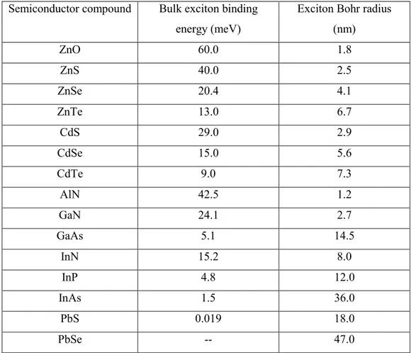
Table 2.1. Bulk exciton binding energies and exciton Bohr radii of common II-VI and III-V semiconductor compounds. ... 19 Table 4.1. Fluorescence decay components of the donor 4 ML NPLs. ... 98 Table 4.2. Fluorescence decay components of the acceptor 5 ML NPLs. ... 99 Table 4.3. Amplitude averaged fluorescence lifetimes of the donor and acceptor NPLs for the samples having varying A:D ratio. Predicted NRET rates (ns-1) are also
presented. ... 99 Table 4.4. Molecular weights and PDIs of all polymers. ... 119 Table 4.5. Fluorescence lifetime components of the solid thin film samples measured at the peak emission wavelength (453 nm). ... 142 Table 4.6. Fluorescence lifetime components of the solid thin film samples measured at the acceptor peak emission wavelength (513 nm). ... 143 Table 4.7. Donor QDs and acceptor NPLs lifetimes (τ), their NRET rates (kNRET) and
efficiencies (ηNRET) with varying D/A ratios. ... 146
Table 4.8. The calculated NRET efficiencies (ηNRET) and enhancement in the ηNRET for
different temperature points. Here, Δ Shift is the shift in the spectral overlap between the
PL spectrum of donor and the extracted absorption spectrum of acceptor with decreasing temperature; ηNRET is the NRET efficiency using amplitude-average
lifetimes; ηNRET-1 is the NRET efficiency calculated using Δ Shift; ηNRET-2 is the NRET
xxxii
temperature is decreased; Δ-0, Δ-1 and Δ-2 are the enhancements in ηNRET, ηNRET-1 and
ηNRET-2, respectively, with respect to the NRET efficiency value at 270 K. ... 152
Table 5.1. Peak external quantum efficiency of the excitonic LEDs and also control devices. ... 184 Table 5.2. Amplitude-averaged fluorescence lifetimes of the QDs in bare-QD, QD/BPhen, QD/TCTA,QD/IrIr(ppy)3:TCTA and QD/ BPhen /Ir(ppy)3:TCTA samples.
... 186 Table 6.1 Fluorescence lifetime components and the corresponding amplitudes for the CdSe/CdS QDs at different pump intensities measured at peak emission wavelength of 626 nm. ... 210 Table 6.2 Fluorescence lifetime components and the corresponding amplitudes for the zinc-blende CdSe QDs at different pump intensities measured at peak emission wavelength of 567 nm. ... 211 Table 6.3 Sulfur to Selenium ratio calculated by the volumes of the core and the shell, measured by XPS and calculated by (6.4) assuming abrupt core/shell interface and calculated by (6.5) assuming alloyed core/shell interface with varying alloy width. . 216 Table 6.4 Analysis of UV-Vis and photoluminescence spectra for the 4 ML CdSe NPLs grown using different growth times. ... 243 Table 6.5 Fluorescence decay components and the fractional emission contributions of the 4 ML CdSe NPLs grown using different growth times (i.e., different lateral areas). ... 246 Table 6.6 Calculated contribution of the fluorescence lifetime components to the total emission of the NPL samples. ... 252 Table 6.7 Calculated and experimental fractions emission contributions of the lifetime components are compared, exhibiting a very well match with the calculation and the experiment. ... 252 Table 6.8 Single- (1PA) and two-photon absorption (2PA) pumped of ASE thresholds of the 4ML CdSe NPLs having different lateral size. ... 256
1
Chapter 1
Introduction
Photonics technology is envisioned to enable key technology platforms to combat some of the most difficult societal challenges of the world including sustainable energy generation, energy efficiency, climate change, environmental sustainability, healthy aging of population, and global security. In the past decade, photonics industry has been rapidly growing, which reached a market volume larger than €350 billion in 2013 and is expected to reach €650 billion by 2020 [1]. Photonics technologies encompass a broad range of application areas, including displays, lighting, communication, healthcare and life sciences, defense technologies, photovoltaics, in all of which rapid innovative solutions and disruptive materials are essentially needed. To this end, newly emerging photonic materials are in high demand, being intensively explored and have strategic importance. Among these materials, solution-processed semiconductor nanocrystals, which are synthesized using low-temperature colloidal epitaxy, represent an important alternative to high-temperature gas-phase epitaxy grown semiconductors. Colloidal nanocrystals bring together low-temperature cheap production, ease of material processability on arbitrary substrates and exciting optoelectronic and material properties. Therefore, semiconductor nanocrystals are expected to challenge conventional semiconductors that have been hampered by low throughput and high cost.
2
Last decade has witnessed the rise of colloidal nanocrystals, which have also recently made their transition from research labs into commercial products. Colloidal nanocrystal-based backlighting, which enlarges the color span of a liquid-crystal display (LCD) TV and enhances the color richness and viewing experience, has attracted an extensive interest from industry (e.g., Sony, 3M, Samsung and Phillips) [2]–[4]. This interest has led to a rapidly growing nanocrystal market, which exceeded $300 million by 2013. According to a recent market forecast, the nanocrystal market is expected to grow over $5 billion in 2020 [5]. This remarkable growth is foreseen dominantly in lighting and display technologies, where electrically driven nanocrystal light-emitting diodes (LEDs) are predicted to have a large impact in the display industry to rival current organic-LED (OLED) based displays. The market predictions also show that nanocrystal-based lasers [6], solar cells [7], transistors [8] and sensors [9] will become appealing for the industry in the coming years as a result of the promising basic research and development efforts. Although colloidal semiconductor nanocrystals can potentially enable next-generation low-cost, large-scale and energy-efficient optoelectronics, there exist both practical and fundamental challenges that need to be addressed to make these materials competitive and competent for practical devices. In this thesis, we have addressed numerous challenges that have existed in the conventional colloidal nanocrystals and in their hybrid systems hindering the achievement of energy-efficient optoelectronics and offered new solutions and understanding.
The colloidal nanocrystals could, in principle, empower lasers that can emit in any color in the visible and infrared [10]. However, to date, nanocrystal lasers have been severely obstructed due to their poor performance making them impractical for feasible real-life applications. The limitation in nanocrystal lasers essentially arises from the dominant Auger recombination [11] that leads to the depletion of the available gain by rapid annihilation of the gain-active electronic species. Another challenge is the small optical gain coefficients in the conventional nanocrystals arising from the small stimulated emission cross-sections in them. Thus, nanocrystals that can simultaneously suppress Auger recombination and achieve large stimulated emission cross-sections are highly desired to accomplish the first practical nanocrystal lasers.
3
Moreover, colloidal nanocrystals and their solid films are exciting for light-harvesting applications such as solar cells [12] and artificial photosynthesis [13] with tunable and broadband light absorption. Yet, ultrashort exciton diffusion lengths (< 20 nm) in the nanocrystal solids make them incompetent for efficient photovoltaics [14]. Nanocrystal solids that can accomplish extended exciton diffusion lengths are crucially required, which can unleash the potential of these materials for efficient light-harvesting.
Additionally, as nanocrystal market forecasts predict, electroluminescent nanocrystal light-emitting diodes will make a niche application for versatile display applications. Although efficient nanocrystal LEDs have been reported based on complex device architectures with multiple charge injection, transport and blocking layers [15], the performance of these electroluminescent devices is deteriorated due to the charge imbalance that detrimentally leads to the charging of nanocrystals and the interfaces in active electroluminescent devices. Furthermore, it is difficult to control the exciton formation zone, thus excitons that are formed outside the nanocrystals result in unfavorable efficiency droops in these devices [16]. Thus, it is needed to understand and control charge and exciton processes in nanocrystal LEDs. Also, exciton recycling is crucially needed to overcome the undesired nonradiative processes, but it has not been systematically studied before.
In this thesis, we have proposed, developed and demonstrated novel energy-efficient optoelectronic devices, based on the engineered excitonic properties of low-dimensional colloidal semiconductors. For this, we have designed and developed new-generation heterostructured semiconductor nanocrystals and their hybrid assemblies, systematically investigated their optical, electronic and material properties and tailored these materials for desired photonic response. As we have explored in this thesis, new-generation designer colloidal nanocrystals can potentially overcome the long standing problems of conventional colloidal nanocrystals. This could therefore potentially lead to efficiency breakthroughs in their optoelectronic devices.
4
Here, we have achieved remarkable optical gain performance using CdSe/CdS nanoplatelets that accomplish record high optical gain coefficients among all-solution processed semiconductors [17]. Our work has unleashed the great potential colloidal nanoplatelets as lasing media for the first time. We also developed the first all-colloidal nanocrystal lasers that showed record low frequency up-converted lasing threshold. These all-solution processed nanocrystal lasers are highly interesting for under-skin therapy and bio-imaging applications [18]. Moreover, developing the close-packed assemblies of the atomically-flat colloidal CdSe colloidal nanoplatelets, we have uncovered an ultrafast exciton transfer process [19]. This finding suggests the possibility of ultralong exciton diffusion lengths (>100 nm) in self-assembled nanoplatelet solids, which could open up new ways to harvest sunlight efficiently in colloidal nanocrystals solar cells. In addition, we have demonstrated organic-inorganic hybrids of colloidal quantum dots that achieve highly efficient exciton funneling transfer at the nanoscale [20]. These hybrids enabled exciton recycling in the nanocrystal light-emitting diodes, which substantially enhance their power conversion efficiencies and offer an efficient means to tackle the challenge of exciton leakage problem in nanocrystal light-emitting diodes [21]. Overall, the findings of this thesis have contributed to a new understanding of optical and excitonic properties in next-generation colloidal semiconductors, helping to form a bridge between the fields of excitonics and optoelectronics to achieve solution-processed and energy-efficient optoelectronics.
1.1 Organization of the thesis
In Chapter 2, we introduce colloidal semiconductor nanocrystals and discuss their optical properties that are essentially dominated by excitonic processes. We also discuss the basics of optical gain and elucidate the gain mechanism in conventional nanocrystals.
In Chapter 3, we present frequently used experimental methods in this thesis, which include steady state and time-resolved fluorescence spectroscopies. Furthermore, we explain how we characterized colloidal gain media for their gain threshold and modal