IEEE PHOTONICS TECHNOLOGY LETTERS, VOL. 10, NO. 5, MAY 1998 707
100-GHz Resonant Cavity Enhanced
Schottky Photodiodes
B. M. Onat,
Student Member, IEEE,M. G¨okkavas, E. ¨
Ozbay, E. P. Ata, E. Towe,
and M. S. ¨
Unl¨u,
Senior Member, IEEEAbstract— Resonant cavity enhanced (RCE) photodiodes are promising candidates for applications in optical communications and interconnects where ultrafast high-efficiency detection is de-sirable. We have designed and fabricated RCE Schottky photodi-odes in the (Al, In) GaAs material system for 900-nm wavelength. The observed temporal response with 10-ps pulsewidth was lim-ited by the measurement setup and a conservative estimation of the bandwidth corresponds to more than 100 GHz. A direct com-parison of RCE versus conventional detector performance was performed by high speed measurements under optical excitation at resonant wavelength (895 nm) and at 840 nm where the device functions as a single-pass conventional photodiode. A more than two-fold bandwidth enhancement with the RCE detection scheme was demonstrated.
Index Terms— High-speed, photodetector, resonant cavity en-hancement, Schottky photodiode.
I. INTRODUCTION
H
IGH-SPEED photodetectors for today’s high-perform-ance optical communication, signal processing, and mea-surement systems must have fast responses, and high sensi-tivities. For high-bandwidth detectors, the optimized structure typically requires a thin absorption region. However, utilizing a thin absorption region necessarily results in reduced quantum efficiency at wavelengths where the absorption coefficient of the semiconductor material is relatively small. Although photodetectors with bandwidths exceeding 200 GHz have been successfully fabricated [1], the bandwidth-efficiency product has remained limited by the material properties. In Schottky photodiodes, optical losses in the metal contact further limit the quantum efficiency for top illuminated devices. Efforts to increase the device responsivity have been pursued by utilizing semi-transparent [1], [2] Schottky contacts.Over the past several years a new family of optoelectronic devices has emerged whose performance is enhanced by plac-ing the active device structure inside a Fabry–Perot resonant microcavity [3]. In such resonant cavity enhanced (RCE) structures, the device functions largely as before, but is subject to the effects of the cavity. In RCE detectors, the quantum
Manuscript received December 10, 1997. This work was supported by the Office of Naval Research under Grant N00014-96-1-0652, by the National Science Foundation under Grant INT-96-01770, and by Turkish Scientific and Technical Research Council under Project EEEAG-156.
B. M. Onat, M. G¨okkavas, and M. S. ¨Unl¨u are with Boston University, Department of Electrical and Computer Engineering, Boston, MA 02215 USA. E. ¨Ozbay and E. P. Ata are with the Physics Department at Bilkent University, Ankara 06533, Turkey.
E. Towe is with University of Virginia, Charlottesville, VA 22903 USA. Publisher Item Identifier S 1041-1135(98)03042-0.
efficiency is dramatically enhanced at the resonant wavelength for thin absorbing layers allowing for a drastic improvement in the bandwidth-efficiency product [3]. The RCE detectors with single layer top mirrors also benefit from post-growth adjustment of the resonant wavelength by simply recessing the top layer [3], [4]. The RCE detection scheme is particularly attractive for Schottky type photodetectors since the semi-transparent Schottky contact can also function as the top reflector of the cavity. High-speed RCE Schottky photodiodes with semi-transparent top contacts have demonstrated 20-GHz bandwidths [5].
In this letter, we present experimental results on the high-speed properties of 100-GHz RCE Schottky photodiodes with semi-transparent top metal contacts. The photodiodes were designed and fabricated for 900-nm wavelength and we have measured temporal responses of 10-ps full-width at half-maximum (FWHM). These results were measurement setup limited and a conservative estimation of the 3-dB bandwidth corresponds to more than 100 GHz [6]. Also, RCE versus conventional device performance was directly compared by high-speed measurements under optical excitation at resonant wavelength (895 nm) and at 840 nm, where the device func-tions as a single-pass conventional detector due to intracavity GaAs absorbtion.
II. DEVICE STRUCTURE
The most important response speed limitation in hetero-junction photodiodes is the transit time across the depleted region. Other speed limitations such as capacitance, diffusion and trapping can be avoided by designing small area detectors with depleted absorption regions and graded heterointerfaces. For transit time limited conventional detectors with thin absorption regions, the bandwidth-efficiency product is [7]:
(1) which is independent of the design parameters and can be perceived as a fundamental speed limitation. For antireflection coated ( 0) GaAs detectors operating at around 900-nm wavelength 10 cm 6 10 cm/s) this product is less than 30 GHz.
In RCE detectors, a high quantum efficiency can be obtained for thin absorption layers and bandwidth-efficiency product is no longer limited by material parameters. Also, a thin absorber can be placed in the otherwise transparent depletion region of the photodiode at an optimized position to equalize transit
708 IEEE PHOTONICS TECHNOLOGY LETTERS, VOL. 10, NO. 5, MAY 1998
Fig. 1. Schematic cross section of the RCE Schottky photodiode.
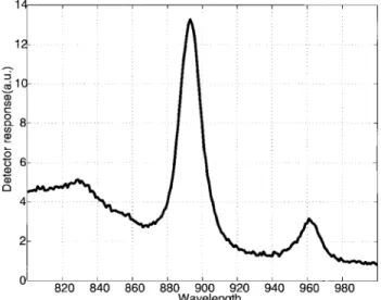
Fig. 2. Measured spectral response of RCE Schottky photodiodes.
times for electrons and holes. Thus, the transit time limited bandwidth will benefit from the sum of the drift velocities instead of being limited by the slower carrier for given depletion width [3]. The overall expected improvement in the bandwidth-efficiency product is nearly threefold for GaAs photodiodes with 10 10 m junction area [7].
The RCE Schottky photodiode layer structure was grown on a GaAs substrate by molecular beam epitaxy (MBE) (Fig. 1). The cavity is formed by a GaAs–AlAs DBR bottom reflector and a semi-transparent Au contact on top. The InGaAs absorption layer has an In mole fraction less than 10% and both heterojunctions were linearly graded for 25 nm to avoid carrier trapping. The total absorption region thickness of 130 nm was utilized to eliminate the standing-wave effect [3] in the cavity. The position of the absorption layer in the depletion region is optimized to yield minimum transit time for electrons and holes as described earlier. Devices were fabricated by stan-dard photolithography with mesa isolation and a Au air-bridge connecting the top contact to a coplanar transmission line
(a)
(b)
Fig. 3. (a) Measured pulse response of the RCE Schottky photodiode mea-sured at the resonant wavelength. The meamea-sured FWHM is 10 ps. (b) Meamea-sured pulse response of the same device at 840-nm wavelength demonstrating a FWHM of 13 ps.
designed for on wafer microwave characterization. A 20-nm-thick Au contact and a 200-nm Si N coating were used based on the optimum values obtained from simulation results [6].
III. EXPERIMENTAL RESULTS
The resonant peak is observed at 895 nm with a sixfold resonant enhancement (Fig. 2) [6]. The measured peak quan-tum efficiency was about 20%, which is significantly less than the theoretical value. The discrepancy is due to the red shift in the center wavelength of the bottom DBR mirror resulting in a 60% bottom reflectivity. Optimized device structure is expected to yield 70% quantum efficiency.
High-speed measurements were implemented by utilizing a picosecond mode-locked Ti:sapphire laser. The devices were illuminated using a single-mode fiber on a microwave probe station and the resulting pulses were observed on a 50-GHz sampling scope. For a direct comparison of the high-speed
ONAT et al.: 100-GHz RESONANT CAVITY ENHANCED SCHOTTKY PHOTODIODES 709
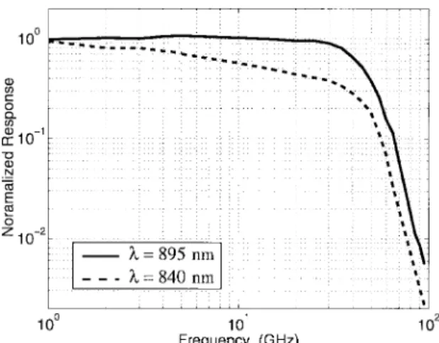
Fig. 4. FFT of the as-measured response with the RCE Schottky photodiode at resonance (900 nm) and at off-resonance (840 nm).
response of RCE and conventional photodiodes, we performed measurements at 895- and 840-nm wavelength on a 10 10 m detector. We measured a 10-ps FWHM at 895 nm [Fig. 3(a)] where only the InGaAs region is absorbing the light excitation (Fig. 1) and the device functions as a RCE photodiode. The measured FWHM was 13 ps at 840 nm [Fig. 3(b)] where the entire InGaAs–GaAs region is absorbing and the device functions largely as a conventional photodiode. The difference appears to be only 30%, however these mea-surements are limited by the speed of the sampling scope. The measured pulsewidth can be approximated as [8]:
(2) This is very accurate for Gaussian pulses and a good ap-proximation for the actual measurements. Considering a 9-ps FWHM for the 50-GHz scope [8], and the laser pulsewidth of 1.2 ps, the device speed was estimated to be 4.1 ps at 895 nm and 9.3 ps at 840 nm. This is a conservative estimate since the microwave components and laser timing jitter also contribute to the measured pulsewidth. The bandwidth of the 900- and 840-nm responses is in excess of 100 and 47 GHz, respectively. This demonstrates a more than two-fold bandwidth enhancement with the RCE detection scheme as predicted by numerical simulations [7]. Together with the 3-fold increase in the efficiency (Fig. 2), the bandwidth-efficiency product of the devices is improved by a factor of 6 at resonance.
To verify the transit-time limited operation of these devices we measured the response speed of various size devices. The devices with mesa sizes smaller than 20 30 m were not capacitance limited showing temporal responses around
10-ps FWHM. The capacitance of the 10 10 m area device was 40 fF corresponding to a RC limited bandwidth of more than 200 GHz. The theoretical expected transit time limited FWHM at 895-nm operation is 3 ps in good agreement with experiment.
The fast Fourier transforms (FFT) of the as-measured re-sponse with the RCE Schottky photodiode under resonance (895 nm) and off-resonance (840 nm) are displayed in Fig. 4. Two data sets, first with a 48.9-fs sampling interval, and the second with a 1-ns total time interval were utilized. Thus, for each FFT calculation of the individual measurements, we obtained an accurate frequency response from 1 to 100 GHz. The gradual drop in the frequency response at 840 nm can be explained by the diffusion of carriers generated in the neutral GaAs region. This effect is also observed in the temporal response [Fig. 3(b)] as a long tail. The frequency response at 895 nm is almost perfectly flat with a 3-dB bandwidth limited by the measurement setup.
IV. CONCLUSION
We have demonstrated a high-speed top illuminated RCE Schottky photodiode with semi-transparent Au contact. The 10-ps FWHM pulses measured on the scope are estimated to represent 4.1-ps FWHM impulse response, corresponding to a 3-dB bandwidth of more than 100 GHz.
REFERENCES
[1] E. ¨Ozbay, K. D. Li, and D. m. Bloom, “2.0 psec, 150 GHz GaAs mono-lithic photodiode and all-electronic sampler”, IEEE Photon. Technol.
Lett., vol. 3, pp. 570–572, 1991.
[2] R.-H. Yuang, J.-I. Yuang, J.-I. Chyi, Y.-J. Chan, W. Lin, and Y.-K. Tu, “High-responsivity InGaAs MSM photodetectors with semi-transparent Schottky contacts,” IEEE Photon. Technol. Lett. vol. 7, pp. 1333–1335, Nov. 1995.
[3] M. S. ¨Unl¨u and S. Strite, “Resonant cavity enhanced (RCE) photonic devices,” J. Appl. Phys. Rev., vol. 78, no. 2, pp. 607–639, 1995. [4] S. Murtaza, I.-H. Tan, J. E. Bowers, E. L. Hu, K. A. Anselm, M.
R. Islam, R. V. Chelakara, R. D. Dupuis, B. G. Streetman, and J. C. Campbell, “High-finesse resonant-cavity photodetectors with an adjustable resonance frequency,” J. Lightwave Technol., vol. 14, pp. 1081–1089, 1996.
[5] E. ¨Ozbay, M. S. Islam, B. M. Onat, M. G¨okkavas, O. Aytur, G. Tuttle, E. Towe, R. H. Henderson, M. S. ¨Unl¨u, “Fabrication of high-speed resonant cavity enhanced Schottky photodiodes,” IEEE Photon. Technol. Lett., vol. 9, pp. 672–674, May 1991.
[6] M. G¨okkavas, B. M. Onat, E. ¨Ozbay, M. S. Islam, E. P. Ata, E. Towe, G. Tuttle, and M. S. ¨Unl¨u, “Ultrafast resonant cavity enhanced Schottky photodiodes,” in Proc. IEEE Lasers and Electroptics Soc., 1997 Annu.
Meet., San Fransisco CA, Nov. 10–13 1997, vol. 1, pp. 160–161.
[7] M. S. ¨Unl¨u, B. Onat, and Y. Leblebici, “Transient simulation of het-erojunction photodiodes, part II: Analysis of resonant cavity enhanced photodetectors,” J. Lightwave Technol., vol. 13, pp. 396–405, Mar. 1995. [8] K. Rush, S. Draving, and J. Kerley, “Characterizing high-speed