Determination of energy-band offsets between GaN and AlN
using excitonic luminescence transition in AlGaN alloys
A. N. Westmeyer, S. Mahajan, and K. K. Bajaja兲
Department of Chemical and Materials Engineering, Arizona State University, Tempe, Arizona 85287 J. Y. Lin and H. X. Jiang
Department of Physics, Kansas State University, Manhattan, Kansas 66506 D. D. Koleske
Sandia National Laboratories, Albuquerque, New Mexico 87185 R. T. Senger
Department of Physics, Bilkent University, 06800 Ankara, Turkey
共Received 5 April 2005; accepted 18 November 2005; published online 9 January 2006兲
We report the determination of the energy-band offsets between GaN and AlN using the linewidth 共full width at half maximum兲 of an extremely sharp excitonic luminescence transition in AlxGa1−xN alloy with x = 0.18 at 10 K. Our sample was grown on C-plane sapphire substrate by metal-organic chemical-vapor deposition at 1050 ° C. The observed value of the excitonic linewidth of 17 meV is the smallest ever reported in literature. On subtracting a typical value of the excitonic linewidth in high-quality GaN, namely, 4.0 meV, we obtain a value of 13.0 meV, which we attribute to compositional disorder. This value is considerably smaller than that calculated using a delocalized exciton model关S. M. Lee and K. K. Bajaj, J. Appl. Phys. 73, 1788 共1993兲兴. The excitons are known to be strongly localized by defects and/or the potential fluctuations in this alloy system. We have simulated this localization assuming that the hole, being much more massive than the electron, is completely immobile, i.e., the hole mass is treated as infinite. Assuming that the excitonic line broadening is caused entirely by the potential fluctuations experienced by the conduction electron, the value of the conduction-band offset between GaN and AlN is determined to be about 57% of the total-band-gap discontinuity. Using our model we have calculated the variation of the excitonic linewidth as a function of Al composition in our samples with higher Al content larger than 18% and have compared it with the experimental data. We also compare our value of the conduction-band offset with those recently proposed by several other groups using different techniques. © 2006
American Institute of Physics.关DOI:10.1063/1.2158492兴
INTRODUCTION
During the past few years, an enormous amount of effort of the semiconductor research community has been devoted to the study of the structural, electronic, and optical proper-ties of III–V nitrides, their alloys, and their heterostructures. The motivation for this effort has been provided by applica-tions in a variety of electronic and optoelectronic devices, such as high-power field-effect transistors, light-emitting di-odes, and laser diodes operating in the visible to ultraviolet range of the electromagnetic spectrum. These devices have been fabricated using metal-organic chemical-vapor deposi-tion 共MOCVD兲 and molecular-beam epitaxy 共MBE兲 growth techniques, and their performance characteristics have been studied in considerable detail. A number of these devices are now commercially available. In addition, a large number of experimental and theoretical investigations have been carried out to gain a better understanding of the fundamental prop-erties of these materials. Although we have obtained a wealth of information during the past few years, a full
understand-ing of the various mechanisms involved in the operation of these devices and of the fundamental properties of these ma-terial systems is still lacking.
Several groups have investigated the optical properties of an AlGaN alloy system using a variety of characterization techniques such as absorption, photoluminescence excitation 共PLE兲, cathodoluminescence, and photoluminescence 共PL兲 spectroscopies during the past few years. In particular, the variation of the linewidth, defined as the full width at half maximum共兲 of an excitonic transition at low temperatures, as a function of alloy composition in the AlGaN alloy system has been studied by several groups1–4using PL spectroscopy. It is well known that such studies can provide useful infor-mation about the quality of the alloys.5 In their pioneering work, Steude et al.1 studied the optical properties of coher-ently strained AlxGa1−xN alloys 共0艋x艋0.22兲 grown on 共0001兲-oriented sapphire by MOCVD using a variety of characterization techniques such as absorption, transmission, reflection, cathodoluminescence, and PL at low temperatures. In particular, they have measured the variation of as a function of Al concentration 共x兲 at 4 K and found, as ex-pected, that it increases as a function of x.
Following this work, Coli et al.2,3have reported a study a兲Permanent address: Department of Physics, Emory University, Atlanta, GA
30322; electronic mail: [email protected]
JOURNAL OF APPLIED PHYSICS 99, 013705共2006兲
of the variation ofas a function of the Al concentration in AlxGa1−xN alloys using PL spectroscopy at 10 K. In their studies the value of x was varied from 0 to 0.7. Their samples were grown by low-pressure MOCVD on sapphire 共0001兲 substrates. They found that the values ofincreased as a function of x, as expected, but are somewhat smaller than those measured by Steude et al.1 In addition, the mea-sured values of are close to those calculated by Lee and Bajaj,6who assumed completely random alloys and delocal-ized excitons. Both Steude et al.1and Coli et al.,2,3however, did not provide any information on the structural character-istics of their samples. Pendlebury et al.4have also measured the variation ofwith Al concentration in AlxGa1−xN using PL spectroscopy at 4 K. Their samples were grown by MOCVD on C-plane sapphire substrates and the Al concen-tration was varied from 0 to 0.5. Their values ofare larger than those reported by Coli et al.2,3 and are comparable to those measured by Steude et al.1They also performed PLE measurements and measured the variation of Stokes’s shift, i.e., the difference in energy between the peak positions in PLE and PL and find that it increases as a function of Al concentration, thus suggesting a strong localization of exci-tons in their samples. Recently, Cho et al.7have investigated the optical properties of AlxGa1−xN epilayers using a variety of characterization techniques such as PL, PLE, and time-resolved PLE. Their samples were grown by MOCVD on 共0001兲-oriented sapphire substrates and the value of the Al concentration was varied from 0 to 0.6. They measured the variation of the energy of the PL peak position as a function of temperature and observed a well-known “S-shaped” be-havior 共decrease-increase-decrease兲. In addition, the exci-tonic linewidth follows an “inverted S-shaped” behavior 共increase-decrease-increase兲 as a function of temperature. These are well known signatures of emission due to localized excitons. Cho et al.7 also did not provide any information concerning the structural properties of their epilayers.
In this paper, we present results of structural and low-temperature PL measurements on an AlxGa1−xN sample with Al concentration x = 0.18. We use this information to calcu-late the values of the band offsets between GaN and AlN using a model where the holes are completely localized. We have used this model to calculate the variation of the exci-tonic linewidth as a function of Al concentration in our samples which have Al content larger than 18% and have compared it with the experimental data.
EXPERIMENTAL DETAILS
Our sample with 18% Al concentration was grown by MOCVD and consisted of a thin 共10 nm兲 GaN nucleation layer grown on C-plane sapphire at 550 ° C, a 1m-thick GaN layer grown on the nucleation layer at 1050 ° C, and a 2000-Å-thick AlxGa1−xN layer also grown at 1050 ° C. No cap layer was used in this sample. Several analytical and structural measurements were performed using Rutherford backscattering共RBS兲, x-ray diffraction 共XRD兲, and transmis-sion electron microscopy共TEM兲. All PL measurements were performed at 10 K using a single-photon counting detection system together with a microchannel-plate photomultiplier
tube, with the detection capability ranging from 185 to 800 nm and an overall resolution of 0.2 meV. The wave-length of the exciting radiation was 292 nm, and the PL sig-nals were collected in reflecting mode at an incident angle of about 30°.
RESULTS AND DISCUSSION
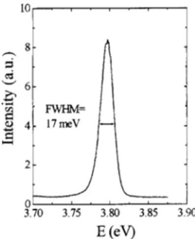
The value of the Al concentration x in our sample was determined using Rutherford backscattering and x-ray-diffraction techniques. The latter measurement did not show any atomic ordering. This result was confirmed by examin-ing the 关101¯0兴 zone-axis diffraction pattern 共ZADP兲, where the 关0001兴 spot cannot arise due to double diffraction. Our TEM results indicate the presence of composition modula-tions along the 关0001兴 direction with a period of 共1.1±0.7兲 nm. In Fig. 1, we display the PL spectrum of AlxGa1−xN for x = 0.18 at 10 K.
During the past 20 years a number of groups5 have re-ported calculations ofas a function of alloy composition in completely disordered semiconductor alloys. The results of these calculations, as well as their comparison with the ex-perimental data in a number of III–V and II–VI alloys, have been reviewed recently.5 We will compare our measured value ofwith those calculated using the model of Lee and Bajaj.6 Using a quantum statistical approach, they obtained the following expression for:
= 0.410, 共1兲 where 0= dEg共x兲 dx
冋
8 ln共2兲x共1 − x兲Vc 共4/3兲Rex3册
1/2 . 共2兲Here Vc is the volume of the primitive cell, dEg共x兲/dx
de-scribes the variation of the energy of the band gap with alloy composition, Rex=0ប2/e2 is the Bohr radius, =共1/me
+ 1 / mh兲−1 is the reduced mass, me and mh are the electron
and the hole mass, respectively, and0is the static dielectric constant. The values of meand0in AlxGa1−xN used in our calculations are obtained from those of GaN and AlN 共Ref. 2兲 by linear interpolation, namely,
FIG. 1. PL spectrum of the Al0.18Ga0.82N sample at 10 K.
me共x兲
m0
= 0.22共1 − x兲 + 0.33x 共3a兲
and
0共x兲 = 9.7共1 − x兲 + 6.3x. 共3b兲
The values of the hole masses associated with the topmost valence bands in GaN and AlN are not reliably known. A number of attempts, however, to determine the value of the average hole mass of the topmost valence band in GaN have been made and are reviewed by Vurgaftman et al.8 and by Vurgaftman and Meyer.9 These values range from 0.3m0 to 2.2m0. They suggest a value of 1.0m0, based on the analysis of the available experimental data. There is practically no experimental information available about the hole mass of the topmost valence band of AlN. In addition, in AlN the crystal-field splitting is negative and thus the topmost va-lence band has a different symmetry than that in GaN. In view of these uncertainties, we use a value of 1.0m0for the hole mass in our sample which has a low共18%兲 Al concen-tration. As the value of the reduced mass is primarily deter-mined by the mass of lighter particle, namely, the electron, this assumption about the hole mass should not introduce any significant error. The volume is Vc共x兲=a03共x兲/
冑
2 where a0共x兲=3.16共1−x兲+3.112x Å is the lattice constant in thebasal plane. The variation of the energy of the band gap
Eg共x兲 with the Al concentration is given as
Eg共x兲 = 共1 − x兲Eg共GaN兲 + xEg共AlN兲 − b共1 − x兲x, 共4兲
where b is the bowing parameter and the values of the energy gaps at 10 K are Eg共GaN兲= =3.504 eV and Eg共AlN兲
= 6.285 eV. The value of the bowing parameter b we used in our calculation is taken to be 0.6 eV.2
As shown in Fig. 1, the line shape of the excitonic tran-sition is almost Gaussian with the value ofof 17.0 meV. In order to consider only the effect of the compositional alloy disorder onwe subtract from 17.0 meV the constant value of the inhomogeneous broadening 共GaN兲, namely, 4.0 meV, a typical value found in many high-quality samples grown on sapphire substrates in our MOCVD reactor. The value ofof 13.0 meV thus obtained is the lowest value of the excitonic linewidth ever reported in AlxGa1−xN with x = 0.18. The value of calculated for this sample using the formalism of Lee and Bajaj6 is 16.5 meV, larger than 13.0 meV. The observed value of the linewidth in our sample is also considerably smaller than the best reported value in literature.2Any deviation from the perfectly random distribu-tion of cadistribu-tions in our sample will only enhance the value of
. It should be pointed out that the measured value of in our sample also contains contributions from other mecha-nisms such as those due to the presence of random electric fields which arise from the significant additional incorpora-tion of ionized impurities due to the presence of Al.
As mentioned earlier, the emission in AlGaN alloys at low temperatures is primarily due to highly localized exci-tons. Such is also the case in a number of other semiconduc-tor alloys such as InGaP,10 GaAsN,11 InGaAsN,12 and GaAsSbN.13The microscopic nature of excitonic localization by potential fluctuations and/or defects in alloys is not
known. To simulate the exciton localization, Zeman et al.10 assumed complete localization of the hole共namely, the hole mass was treated as infinite兲 in InGaP layers lattice matched to GaAs and explained their data on the variation of the diamagnetic shift of the localized excitons with magnetic field at low temperatures. A similar assumption has also been made recently by Senger et al.13,14to explain their PL data on the variation of the diamagnetic shift of the localized excitons with magnetic field in GaAsSb/ GaAs and GaAsSbN / GaAs quantum well structures, respectively, at low temperatures. It seems that the assumption that the holes are completely localized best describes the situation of exci-tons localized by potential fluctuations and/or defects in the above-mentioned alloys. We believe that such is also the case in AlGaN alloys. If we assume that the holes due to their much larger masses are completely localized, namely, we treat the hole mass as infinite then only the electrons experi-ence the fluctuating potential of the conduction band. The hole clearly does not experience any potential fluctuations. Substituting this value of the hole mass and replacing
dEg/ dx by dEc/ dx we find that for= 13.0 meV, the value
of the conduction-band discontinuity is such that dEc/ dx
= 0.57共dEg/ dx兲.
Recently, Foxon et al.15have studied the behavior of the yellow and blue emissions in GaN and Al0.2Ga0.8N epilayers. The yellow emission is assumed to be due to the recombina-tion of a shallow donor with a deep acceptor due to Ga vacancy, and the blue emission is due to the recombination of a deep donor共presumably As antisite兲 with a shallow ac-ceptor. Using the fact that the positions of deep levels in semiconductors against common vacuum reference level do not change with alloy composition, they determined the value of the conduction-band offset of 0.55 of the band-gap discontinuity. Helman et al.16 have studied the intersubband transitions due to conduction electrons in GaN / AlN quantum wells and have found that a conduction-band offset of 0.64 best explains their data. These two values of the conduction-band offsets are quite close to the value we calculated.
Recently, Vurgaftman and Meyer9have briefly reviewed the results of various calculations of the energy-band offsets between GaN and AlN. Satta et al.17 have pointed out that the energy-band offsets for GaN / AlN and AlN / GaN are dif-ferent. From a detailed treatment of the strain-induced asym-metry at the 共0001兲 polar heterojunctions Bernardini and Fiorentini18have obtained 2.55 eV共93%兲 and 1.9 eV 共69%兲 for the values of the conduction-band offsets for AlN / GaN and GaN / AlN interfaces, respectively. Vurgaftman and Meyer9have also briefly reviewed the results of various mea-surements of the conduction-band offsets between GaN and AlN and found that these values range from 95% to 50% of the total-band discontinuity. Such an enormous disparity among the values of the conduction-band offset is ascribed to differences in effects of strain inhomogeneity, defects, and stoichiometry among the samples used by various groups. The consensus is, however, that the value of the conduction-band offset is larger than the valence-conduction-band offset. Clearly more work needs to be done before one can have confidence in the values of the band offsets in this materials system. It should be pointed out that our value of the conduction-band
offset is the upper limit as the value of 共13.0 meV兲 may contain contributions from mechanisms other than composi-tional potential fluctuations.
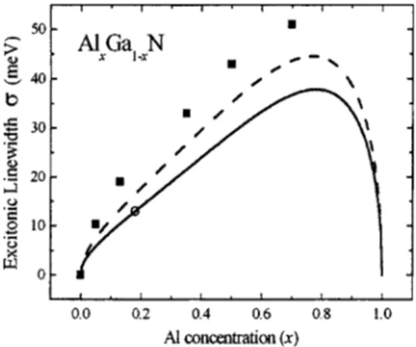
As mentioned earlier, Coli et al.2,3 have measured the variation of as a function of Al concentrations in AlxGa1−xN at 10 K. They found that their measured values of
agree well with those calculated using the formalism of Lee and Bajaj6 that assumes completely random alloys and delocalized excitons. We have now strong evidence that ex-citons are localized in AlGaN alloys.7 We have therefore calculated the variation of as a function of Al concentra-tion in AlxGa1−xN using our model of the localized excitons as described above. We display our results共solid line兲 in Fig. 2 along with the results of a delocalized exciton model 共dashed line兲 and the experimental data 共solid squares兲 of Coli et al.3We find that the values of obtained using the localized exciton model are considerably smaller than those calculated using the delocalized model and the experimental values. This is not surprising. It is well known that the growth of AlGaN alloys with higher values of Al concentra-tion always leads to addiconcentra-tional incorporaconcentra-tion of impurities and defects, larger strain inhomogeneities, and possibly more clustering. The effects of these imperfections on the value of
are not included in our calculations. The difference be-tween our calculated values of using a localized exciton model and the experimental values is suggested to be due to the effects of these imperfections.
It should be pointed out that our approach to determine the values of the energy-band offsets does not involve the use of interfaces between GaN and AlN. Thus, our values are free from the uncertainties introduced by the presence of strain inhomogeneities, defects, and clustering at the inter-faces. It is therefore more meaningful to compare our values of the energy-band offsets with those determined by Foxon
et al.15using radiative recombination between different cen-ters in bulk AlGaN. Even though energy-band offsets are defined when two different semiconductors are brought in contact, the values determined by using bulk properties may
be closer to their intrinsic values. As mentioned earlier our sample exhibits composition modulation along the direction of growth and is of high structural quality. There may be similar composition modulations in the plane perpendicular to the growth direction as well. It is reasonable to assume that these composition modulations play an important role in completely localizing the hole at low temperatures.
CONCLUSION
We have measured the value of the linewidth of an ex-citonic transition in an AlxGa1−xN alloy with x = 0.18 using PL spectroscopy at 10 K. Our sample was grown on 共0001兲-oriented sapphire substrate by MOCVD at 1050 ° C. The value of the observed excitonic linewidth共13.0 meV兲 in this sample is the lowest ever reported in literature. It is signifi-cantly smaller than the value calculated using the delocalized exciton model of Lee and Bajaj and is the lowest value re-ported in the literature. The excitons are known to be strongly localized in this alloy system, and we have simu-lated this localization by assuming that the hole, being much more massive than the electron, is completely immobilized. In other words we treat its mass as infinite. Considering now that the excitonic linewidth is entirely caused by the potential fluctuations experienced by the electron, the value of the conduction-band discontinuity is determined to be 57% of the energy-band-gap difference. This value is similar to those recently found in GaN / AlN structures by some other groups.
ACKNOWLEDGMENTS
One of us 共K.K.B.兲 would like to thank Professor S. Mahajan for his kind and generous hospitality during his stay at Arizona State University. The support of this work by NSF and AFOSR is gratefully acknowledged.
1G. Steude, B. K. Meyer, A. Göldner, A. Hoffmann, F. Bertram, J.
Chris-ten, H. Amano, and I. Akasaki, Appl. Phys. Lett. 74, 2456共1999兲.
2G. Coli, K. K. Bajaj, J. Li, J. Y. Lin, and H. X. Jiang, Appl. Phys. Lett. 78,
1829共2001兲.
3G. Coli, K. K. Bajaj, J. Li, J. Y. Lin, and H. X. Jiang, Appl. Phys. Lett. 80,
2907共2002兲.
4S. T. Pendlebury et al., Phys. Status Solidi A 188, 871共2001兲. 5K. K. Bajaj, Mater. Sci. Eng., R. 34, 59共2001兲.
6S. M. Lee and K. K. Bajaj, J. Appl. Phys. 73, 1788共1993兲.
7Y. H. Cho, G. H. Gainer, J. B. Lam, J. J. Song, W. Yang, and W. Jhe, Phys.
Rev. B 61, 7203共2000兲.
8I. Vurgaftman, J. R. Meyer, and L. R. Ram-Mohan, J. Appl. Phys. 89,
5815共2001兲.
9I. Vurgaftman and J. R. Meyer, J. Appl. Phys. 94, 3675共2003兲. 10J. Zeman, G. Martinez, K. K. Bajaj, I. Krivorotov, and K. Uchida, Appl.
Phys. Lett. 77, 4335共2000兲.
11F. Saidi, F. Hassen, H. Maaref, L. Auvray, H. Dumont, and Y. Monteil,
Mater. Sci. Eng., C 21, 245共2002兲.
12L. F. Bian, D. S. Jiang, P. H. Tan, S. L. Lu, B. Q. Sun, L. H. Li, and J. C.
Harmand, Solid State Commun. 132, 707共2004兲.
13R. T. Senger et al., Appl. Phys. Lett. 81, 2614共2003兲. 14R. T. Senger et al., Appl. Phys. Lett. 81, 5425共2003兲.
15C. T. Foxon, S. V. Navikov, L. X. Zhao, and I. Harrison, Appl. Phys. Lett.
83, 1166共2003兲.
16A. Helman et al., Appl. Phys. Lett. 83, 5196共2003兲.
17A. Satta, V. Fiorentini, A. Bosin, and F. Meloni, Mater. Res. Soc. Symp.
Proc. 395, 515共1996兲.
18F. Bernardini and V. Fiorentini, Phys. Rev. B 57, R9427共1998兲.
FIG. 2. Variation of the excitonic linewidth共兲 as a function of Al concen-tration共x兲. The solid and dashed curves are calculated using localized and free exciton models, respectively. The solid squares are the experimental data given in Ref. 3. The open circle denotes the value for the current sample.