AN ALTERNATIVE APPROACH TO DESIGN LUMPED ELEMENT
DELAY EQUALIZERS
Metin ŞENGÜL
Kadir Has University, Dept. of Electrical and Electronics Engineering, Faculty of Engineering and Natural Sciences, 34083, Cibali-Fatih, Istanbul, Turkey
Tel: +90-212-533-6532, Fax: +90-212-533-4327 [email protected]
Abstract: In this paper, an algorithm has been proposed to design lumped element delay equalizers which is considered as a single block as opposed to the existing methods in literature. Then after obtaining the desired delay performance, the designed delay equalizer is divided and realized as cascaded first-order and/or second-order all-pass circuits. An example is given to illustrate the utilization of the proposed algorithm.
Keywords: Delay equalizer, real frequency technique, lossless network, passive network.
1. Introduction
One of the very important parts of analog filter design is the group delay correction. In modern
communications and signal processing
applications often filters are required, which must satisfy group delay specifications. In literature, there are several approaches to design group delay equalizers for analog filters [1-2]. One of the most common methodologies is to employ a group delay equalizer (all-pass) to correct the group delay of an amplitude function.
For practical applications, first and second order group delay equalizer tables are often used [3], analytical methods are not often preferred.
In literature, different design procedures have been developed to get the optimum group delay response, such as genetic algorithms [4], adaptive filters [5], quasi-all-pass filters [6] and all-pass based equalizers [7], [8-13]. All-pass filters are very important and useful circuits employed in several applications [8], [14].
In this paper, a semi-analytic approach (real frequency technique, RFT) has been utilized to design delay equalizers. After obtaining describing polynomials, delay equalizer has been realized as cascaded first-order and/or second-order all-pass two-port circuits. So in the next section, characterization of lossless two-ports is summarized, then realization of all-pass sections is explained.
2. Characterization of lossless two-ports
Assume that the delay equalizer is a lumped-element lossless two-port like the one shown in Fig. 1, then the scattering matrix can be written as [15]:
) ( ) ( ) ( ) ( ) ( 1 ) ( ) ( ) ( ) ( ) ( 22 21 12 11 p h p f p f p h p g p S p S p S p S p S (1)
where g(p), h(p) and f( p) are real polynomials in complex frequency p j , is a constant and
) ( p
g is a strictly Hurwitz polynomial. The three polynomials g(p), h(p),f( p) are related by the Feldtkeller equation as ) ( ) ( ) ( ) ( ) ( ) (p g p h ph p f p f p g . (2)
Figure 1. Lossless two-port terminated by resistance R From (1), the transfer scattering coefficient S21(p)
is written as ) ( ) ( ) ( 21 p g p f p S (3)
where the polynomial f( p) is formed by using the transmission zeros of the two-port.
An all-pass circuit has a constant gain curve for all frequencies. To be able to realize this property, the poles and zeros of the transfer function must be placed
symmetrically about the j -axis. There is a zero in the right-half plane for each pole in the left-half plane. Namely all-pass circuits are non-minimum phase.
Since a delay equalizer is an all-pass circuit, then the polynomial f( p) must be selected as
) ( )
(p g p
f . As a result, the polynomial h( p) is zero from (2), i.e., h( p) 0. So to be able to completely describe a delay equalizer, it is enough to have the Hurwitz polynomial g( p), then the element values of the delay equalizer can be calculated via the polynomial g( p). So in the next section, let us see the realizations of all-pass transfer functions.
3. Realizations of all-pass transfer
functions
Consider the circuit of Fig. 2. Let the all-pass transfer function S21(p) be written as from (3) under the condition of f(p) g( p):
Figure 2. Lossless two-port as an all-pass circuit
m n m n A n m n m A c p b p c p b p p a p a A p g p g A p S i i i i i i i i 1 1 ) ( ) ( ) ( ) ( ) ( ) ( ) ( 2 2 21 (4)
where A is the gain, g( p) is a strictly Hurwitz polynomial; a , i b and i c are positive real i constants; and m and n are the even and odd parts of g( p), respectively.
Let us calculate the frequency response of the circuit as: ) ( ) ( 21 21(j ) S (j )ej Aej S
with the phase given by:
) ( arctan 2 arctan 2 arctan 2 ) ( 2 X c b a i i i i i (5) where j p m n j X( ) . (6)
Since n /m is an LC impedance function [16], X( ) is the reactance function of n /m.
The group delay can easily be found as:
i i i i i i i i b c c b a a d d D 2 2 2 2 2 2 2 ) ( ) ( 2 2 ) ( (7)
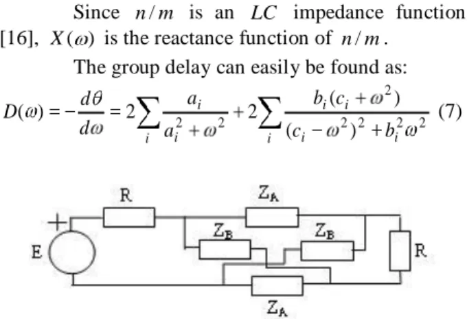
Figure 3. Lossless two-port as an all-pass circuit In literature, there are standard circuit configurations to realize all-pass transfer functions. One of them is the constant-resistance lattice arrangement seen in Fig. 3. If the condition ZAZB R2 is satisfied, then the transfer function can be written as:
A A Z R Z R p S 2 1 ) ( 21 . (8)
If the impedance ZA( p) is LC , then the transfer function is all-pass type. For this circuit, the input impedance is R when output is terminated in R. As a result, any number of such lattice circuits can be cascaded and the overall transfer function is simply the multiplication of individual all-pass transfer functions. A first-order section is realized, if Z is an inductor A and Z is a capacitor with the following conditions: B
pL p ZA( ) , pC p ZB( ) 1 , L R C 2 (9) and in this case, the all-pass transfer function is
pL R pL R p S 2 1 ) ( 21 . (10)
A second-order section can be realized, if Z is an A inductor L in parallel with a capacitor A C , and A Z B is an inductor L in series with a capacitor B C , then B the all-pass transfer function is
A A A A A A C L p RC p C L p RC p p S 1 1 1 1 2 1 ) ( 2 2 21 (11)
and the elements have the following relations
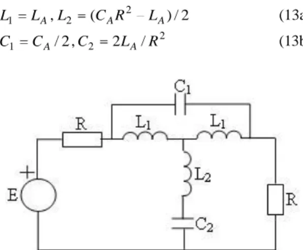
2 R C LB A , 2 R L CB A . (12) The constant-resistance lattice has one disadvantage; its input and output do not have a common ground. But a constant-resistance bridged-T shown in Fig. 4 is a second-order all-pass circuit, and its input and output
have a common ground, where the elements are related to those of the constant-resistance lattice as follows: A L L1 ,L2 (CAR2 LA)/2 (13a) 2 / 1 CA C ,C2 2LA/R2 (13b)
Figure 4. Second-order, constant-resistance bridged-T
all-pass arrangement
In some situations, the inductor L can be 2 negative. In those cases, the three inductors must be replaced by coupled inductors. The bridged-T circuit is also a constant-resistance two-port. Namely any number of them can be cascaded in the same way as constant-resistance lattice.
Now we are ready to propose the following RFT based delay equalizer design algorithm. A similar approach can be developed to design distributed element delay equalizers, if the frequency variable p is changed with the frequency variable via Richards’ transform tanhp , where is the delay of the distributed element.
4. Proposed design algorithm
Inputs:
tdc : Delay data of the circuit in the interested frequency band.
n
G G G
G0, 2, 4,, : Coefficients of the even polynomial n np G p G G p g p g p G 2 2 0 2 ) ( ) ( ) ( .
td : Desired total delay of the cascaded overall system in the interested frequency band.
L
L 2 f and H 2 fH : Lower and
upper frequencies of the band where td is desired.
norm
f and Rnorm : Frequency and impedance normalization number, respectively.
: The stopping criteria of the sum of the squared errors.
Computational Steps:
Step 1: Normalize the frequency band as follows:
norm L normalized L f f ) ( and norm H normalized H f f ) ( .
Step 2: Form polynomial g( p) from initialized even polynomial G(p2) g(p)g( p). Since g( p) is a strictly Hurwitz polynomial, it is constructed from the left-half plane roots of G(p2).
Step 3: Form the even ( m ) and odd ( n ) parts of g( p)
Step 4: Calculate j p m n j X( ) . Then ) ( arctan 2 ) ( X and d d D( ) .
Alternatively, delay of the equalizer can be calculated as d dX X D ( ) ) ( 1 1 2 ) ( 2 .
Step 5: Calculate td (tdc D), and c 2. If c , calculate the element values as follows:
Here the crux of the idea is based on the well-known theorem [17,18] on all-pass circuits: Any all-pass circuit is equivalent to a number of first- and second-order all-pass circuits in cascade.
So if the order of the polynomial g( p) is even, it can be realized as cascaded second-order bridged-T all-pass circuits. If the order is odd, a first-order all-all-pass circuit must also be cascaded. Element values are calculated via (11), (12) and (13) for second-order bridged-T all-pass circuits, and via (9) and (10) for first-order all-pass circuits. Now it is necessary to denormalize the element values as
norm norm n f R L L
2 and norm norm
n R f C C 2 , where Ln and n
C are normalized inductor and capacitor values, respectively. If c , go to the next step, otherwise,
stop.
Step 6: Change the initial coefficients of polynomial )
(p2
G via any optimization routine (in the example, Nelder–Mead optimization method is used. This method is a commonly used nonlinear optimization technique, which is a well-defined numerical method for minimizing an objective function in a many-dimensional space), and go to Step 2.
5. Example
Figure 5. A third-order band-pass filter [16]
In this example, delay equalization of a band-pass filter given in [16] is solved via the proposed algorithm. As in [16], two second-order bridged-T all-pass circuits are connected to the filter to correct the delay. Lower and upper normalized corner frequencies are L(normalized) 3.5 and
5 . 4
) (normalized
H , respectively. Delay data of the
filter ( tdc ) in the frequency band is given in Table I.
Table I. Delay data of the given band-pass filter (sec) tdc 3.5 5.3079 3.6 6.1171 3.7 5.5152 3.8 4.6687 3.9 4.1947 4.0 4.0000 4.1 3.9855 4.2 4.1787 4.3 4.6021 4.4 4.9738 4.5 4.6942
Desired total delay ( td ) in this band is selected as 9.4 second. Initial coefficients of the polynomial G(p2) are calculated from the initials used in [16], so 131590 26705 3 . 2075 1604 . 73 ) ( 2 4 6 2 p p p p G .
After applying the proposed algorithm, the following polynomial g( p) is obtained,
8405 . 362 0009 . 51 3879 . 40 7603 . 2 ) ( 4 3 2 p p p p p g .
This polynomial can be written as a multiplication of two second-order polynomials as
) 1539 . 16 0164 . 1 ( ) 4614 . 22 7439 . 1 ( ) ( 2 2 p p p p p g .
So element values of the constant-resistance bridged-T all-pass circuits can be calculated as explained in Section III. Element values of the first section are L1 0.0776, L2 0.2479,
2867 . 0
1
C , C2 0.1552, and those of the
second section are L1 0.0629, L2 0.4605, 4920
. 0
1
C , C2 0.1258 . Element values found
in [16] are as follows: For section 1: L1 0.0777, 248 . 0 2 L , C1 0.2869, C2 0.1554, and for section 2: L1 0.0623, L2 0.4653, 4965 . 0 1
C , C2 0.1246. The given filter and the designed all-pass circuits are connected as seen in Fig. 6.
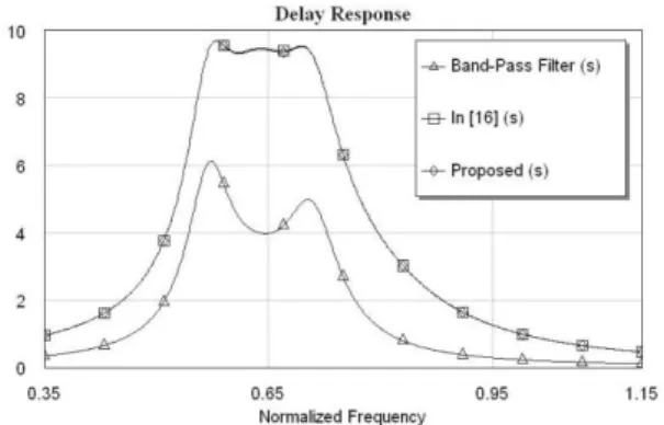
Figure 6. Band-pass filter and cascaded all-pass circuits Delay curves of the band-pass filter and overall system are given in Fig. 7. In the same figure, performance of the overall system given in [16] is added for comparison. It is seen that the delay in the pass-band is nearly constant with a maximum fluctuation less than 10% of the average delay in the pass-band as in [16].
Figure 7. Delay responses of the band-pass filter and overall
system
6. Conclusions
Here an alternative approach to design lumped-element delay equalizer is proposed. During the design, delay equalizer is assumed to be a lossless two-port. The describing polynomial g( p) is optimized until getting the desired total delay performance of the overall cascaded system. Then the polynomial g( p) is written as the product of second-order and/or first-order polynomials. Finally the element values are calculated.
In literature, first-order and/or second-order all-pass sections are designed separately. Namely their delay responses calculated separately. But in the proposed approach, the delay equalizer is considered as a single block, so only one delay response is calculated during the optimization process. After obtaining the desired performance, the single block is divided as first-order and/or second-order sections.
6. References
[1] G. Szentirmai, “The problem of phase equalization”, IRE Trans. on Circ. Theory, vol. 6(3), pp. 272-277, 1959.
[2] A. Henderson, L. Ping, J. I. Sewell, “Extended Remez algorithms for filter amplitude group delay approximation”, IEEE Proceedingsg, vol. 138, no. 3, 1991.
[3] A. Williams, Electronic filter design handbook, McGraw-Hill Inc., 1981.
[4] V. Hegde, S. Pai, W. K. Jenkins, T. B. Wilborn, “Genetic algorithms for adaptive phase equalization of minimum phase SAW filters”, 34th Asilomar Conf. on
Sig. Syst. and Comp., vol. 2, pp. 1649-1652, 29 Oct.-01 Nov. 2000.
[5] B. Farhang-Boroujeny, S. Nooshfar, “Adaptive phase equalization using allpass filters”, IEEE Int. Conf. on Comm., vol. 3, pp. 1403-1407, 23-26 June 1991. [6] H. Baher, M. O’Malley, “FIR transfer functionswith
arbitrary amplitude and phase, with applications to the design of quasi-allpass delay equalizers”, IEEE Int. Symp. on Circ. And Syst., vol. 3, pp. 2489-2491, 7-9 June 1988.
[7] K. Umino, J. Andersen, R. G. Hove, “A novel IIR filter delay equalizer design approach using a personal computer”, IEEE Int. Symp. on Circ. Syst. vol. 1, pp. 137-140, May 1990.
[8] P. A. Regalia, S. K. Mitra, P. P. Vaidyananathan, “The digital allpass filter: A versatile signal processing building block”, Proc. IEEE, vol. 76(1), 1988.
[9] A. G. Deczky, “Equiripple and minimax (Chebyshev) approximations for recursive digital filters”, IEEE Trans. Acoust. Speech Sig. Proc., vol. ASSP-22, pp. 98-111, 1974.
[10] T Inukai, “A unified approach to optimal recursive digital filter design”, IEEE Trans. on Circ. And Syst., vol. CAS-27(7), pp.646-649, 1980.
[11] Antoniou, Digital filters: analysis, design and applications, McGraw-Hill, 1993.
[12] M. Lang, T. I. Laakso, “Simple and robust method for the design of allpass filters using least-squares phase error criterion”, IEEE Trans. on Circ. And Syst.-II: Analog and Dig. Sig. Proc., vol. 41(1), pp. 40-48, 1994.
[13] H. W. Schuessler, P. Steffen, “On the design of allpasses with prescribed group delay”, Int. Conf. on Acoust., Speech Sig. Proc., pp.1313-1316, 1990.
[14] P. Bernhardt, “Simplified design of high-order recursive group-delay filters”, IEEE Trans. Acoust. Speech Sig. Proc., vol. ASSP-28(5), pp. 498-503, 1980.
[15] V. Belevitch, Classical Network Theory. San Francisco, CA, Holden Day, 1968.
[16] O. Wing, Classical Circuit Theory, New York, NY, Springer, 2008.
[17] H. W. Bode, “Network Analysid and Feedback Amplifier Design”, D. Van Nostrand Co., Inc., New York, N.Y., pp. 239-242, 1945.
[18] S. Hellerstein, “Synthesis of All-Pass Delay Equalizers”, IRE Trans. Circuit Theory, vol. 8(3), pp. 215-222, 1961.
Metin ŞENGÜL received his B.Sc. and M.Sc. degrees in Electronics Engineering from Istanbul University, Turkey in 1996 and 1999, respectively. He completed his Ph.D. in 2006 at Işık University in Istanbul, Turkey. He worked as a technician at Istanbul University from 1990 to 1997 and was a circuit design engineer at the R&D Labs of the Prime Ministry Office of Turkey between 1997 and 2000. He was employed as a lecturer and assistant professor at Kadir Has University, Istanbul, Turkey between 2000 and 2010. Dr. Şengül was a visiting researcher at the Institute for Information Technology, Technische Universität Ilmenau, Ilmenau, Germany in 2006 for six months. Currently, he is an associate professor at Kadir Has University, Istanbul, Turkey and working on microwave matching networks/amplifiers, device modeling, circuit design via modeling and network synthesis.