IEEE ELECTRON DEVICE LETTERS, VOL. 32, NO. 6, JUNE 2011 797
An Indium-Free Transparent Resistive
Switching Random Access Memory
K. Zheng, X. W. Sun, J. L. Zhao, Y. Wang, H. Y. Yu, H. V. Demir, and K. L. Teo
Abstract—We report an indium-free transparent resistive
switching random access memory device based on GZO-Ga2O3
-ZnO-Ga2O3-GZO structure by metal–organic chemical vapor
deposition. The memory device shows good transmittance in the visible region and bipolar resistive switching behavior with good cycling characteristics and retention time under room temper-ature. The conduction and resistive switching mechanism was discussed based on filament theory.
Index Terms—GZO, indium free, transparent resistive
switch-ing, ZnO.
I. INSTRUCTION
T
RANSPARENT resistive switching random access mem-ory (TRRAM) device is potentially useful in the fu-turistic transparent electronics. It is meant to be integrated with other transparent electronic devices to produce the so-called see-through system-on-glass [1], which belongs to the domain of macroelectronics. ZnO, with high transmittance in the visible region and tunable conductivity by doping, has been demonstrated to be a good candidate for constructing the TRRAM device due to its abundance in nature, highly evolved growth technologies, and compatibility with complementary metal–oxide–semiconductor technology. On the other hand, Ga-doped ZnO is a promising alternative of indium tin oxide (ITO) with lower cost, resource availability, and nontoxicity. Thus, it is possible to construct an In-free TTRAM device based purely on ZnO, in contrast to previous studies of using ITO electrodes [2], [3].Manuscript received December 23, 2010; revised February 23, 2011; accepted February 28, 2011. Date of publication April 28, 2011; date of current version May 25, 2011. This work was supported by the Advanced Memory Research Program under Grant 092 151 0088 from Singapore Agency for Science, Technology and Research (A*STAR) SERC. The review of this letter was arranged by Editor S. Kawamura.
K. Zheng, Y. Wang, and H. Y. Yu are with the School of Electrical and Electronic Engineering, Nanyang Technological University, Singapore 639798. X. W. Sun is with the School of Electrical and Electronic Engineering, Nanyang Technological University, Singapore 639798, and also with the De-partment of Applied Physics, College of Science, Tianjin University, Tianjin 300072, China (e-mail: [email protected]).
J. L. Zhao is with the Department of Applied Physics, College of Science, Tianjin University, Tianjin 300072, China.
H. V. Demir is with the School of Electrical and Electronic Engineering and the School of Physical and Mathematical Sciences, Nanyang Technological University, Singapore 639798, and also with the Department of Electrical and Electronics Engineering and the Department of Physics, Bilkent University, Ankara 06800, Turkey.
K. L. Teo is with the Department of Electrical and Computer Engineering, National University of Singapore, Singapore 117608.
Color versions of one or more of the figures in this letter are available online at http://ieeexplore.ieee.org.
Digital Object Identifier 10.1109/LED.2011.2126017
Thus, this letter introduces the fabrication of TRRAM device by utilizing ZnO with different Ga doping concentration to con-struct the metal–insulator–metal (MIM) thin-film con-structure. The resistivity of our GZO electrode is about 3× 10⁻⁴Ω· cm [4]. The resistive switching characteristic was investigated, and the conduction mechanism was discussed in detail.
II. EXPERIMENTALDETAIL
All the functional films were fabricated by a homemade metal organic chemical vapor deposition (MOCVD) system without breaking the vacuum. With all layers fabricated by the same MOCVD system, the process is much simplified. Trimethylgallium (TMGa), dimethylzinc (DMZn), and oxygen were used as reaction sources, and nitrogen was employed as the carrier gas for the metal organics. A 200-nm bottom elec-trode (BE) of GZO was deposited on the glass slide substrate at 300◦C with a chamber pressure of 25 torr. Then, multiple insu-lative films of Ga2O3(50 nm)-ZnO (120 nm)-Ga2O3(50 nm)
were subsequently deposited on the BE film at 400◦C with a chamber pressure of 40 torr. Finally, a 200-nm top electrode (TE) array of GZO was deposited with a shadow mask on the insulating layers. The crystal structure of ZnO and GZO was examined by X-ray diffraction (XRD), and the I–V character-istic was also measured.
III. RESULT ANDDISCUSSION
The XRD spectrum of the ZnO film and GZO film deposited was shown in Fig. 1(a). The ZnO film shows a polycrystalline structure with mainly c-axis orientation. With a low doping of Ga and lower growth temperature of 300 ◦C, the GZO film shows similar diffraction peaks but lower intensity and larger full width at half maximum. The inset shows the transmittance of the device stack. From the photo of the device on the logo, we can see that the device exhibits high transparence. The transmittance is approximately 92% on average in the visible region, excluding the glass substrate.
Fig. 1(b) shows the typical bipolar resistive switching charac-teristics of our TRRAM device. The memory cell was initially highly resistive. When a positive voltage was swept from zero to a critical value of 14 V, the current suddenly increases due to the soft breakdown of the ZnO thin film. Under the protection of compliance current of 20 mA, the device turns from high resistive status (HRS) to low resistive status (LRS). When the voltage sweeps in the opposite direction without the compliance current, an abrupt decrease in current takes place at another critical value of 12 V, and the device turns from LRS back
798 IEEE ELECTRON DEVICE LETTERS, VOL. 32, NO. 6, JUNE 2011
Fig. 1. (a) XRD spectrum of ZnO and GZO films in our TRRAM device. The inset is the transmittance of our TRRAM device, with the inset showing seen-through device. (b) Bipolar resistive switching behavior of our device at the 10th and 50th cycles; the inset shows the device structure.
to HRS again. The steady repeating of the aforementioned operation leads to the bistable resistive switching behavior of our device. The variation of voltage as the repeating cycle increases is in an acceptable range, as shown by the 10th and 50th curves.
The resistances of HRS and LRS in 50 switching cycles are shown in Fig. 2(a) to evaluate the reliability of our TRRAM device. Despite the fluctuation of HRS and LRS resistances, the resistance ratio of HRS/LRS is around 102, which is ac-ceptable for practical applications. The retention characteris-tic was measured to test the nonvolatility of our device. As shown in Fig. 2(b), both HRS and LRS resistances vary in a very small range without significant decay after 105 s, which could be expected to perform highly stable storage. It is worth mentioning that the access time for TRRAM can be slower, compared with Si-based RAM devices, as its target application is in macroelectronics.
As shown in Fig. 3, the resistances in HRS and LRS are both independent of the device area, which indicates that it is probably local filamentary conduction but not interface Schot-tky barrier switching that takes place as previous reported [5].
Fig. 2. (a) Ron and Roff in 50 switching cycles at room temperature.
(b) Retention characteristic at room temperature.
Fig. 3. Cell area dependence of Ronand Roff.
For the filament mechanism, the formation of filamentary paths as a soft breakdown in the dielectric material contributes to the set process, whereas the rupture of these filaments constitutes the reset process. For MIM structure with nonmetal
ZHENG et al.: INDIUM-FREE TRANSPARENT RESISTIVE SWITCHING RAM 799
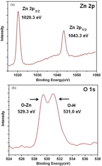
Fig. 4. XPS spectra of ZnO film for (a) Zn 2p and (b) O 1s.
electrode, the eletrochemial migration of oxygen ions is widely regarded as the driving force [6].
To qualitatively analyze the filament in our device, the XPS spectra of the ZnO film for Zn 2p and O 1s core levels were measured (Fig. 4). We can see from Fig. 4(a) that the energy interval between Zn 2p1/2and 2p3/2peaks is 23.0 eV, which
indicates that there is no metallic Zn in the film because of the fully oxidization of Zn. However, that does not exclude the existence of oxygen vacancies in the ZnO film. In Fig. 4(b), the 529.3-eV peak of O 1s is attributed to the O-Zn bonding, whereas the 531.0-eV peak is attributed to the O-H bonding due to the chemisorbed oxygen in the film [7]. This indicates that there is a large amount of nonlattice oxygen ions in the ZnO film, which is responsible for the filament mechanism.
In the initial set process, the positive voltage sweeping drives the positive oxygen vacancies and negative oxygen ions moving to opposite polarities, leading to soft breakdown of dielectric and formation of filament at the interface of the electrode and the insulator. The subsequent breakdown through the whole insulating layer leads to the formation of a complete conductive filament, and the device turns from born HRS to LRS. The hopping of electrons through the filament accounts for the conduction in LRS [6]. In the reset process, the negative voltage sweeping repels the oxygen vacancies and oxygen ions from high and low potentials, respectively, which results in rupture of filament at interface regions and turns the device from LRS to HRS (recovery). Repeating this dynamic process leads to the stable resistive switching controlled by exterior electric signal.
IV. CONCLUSION
In conclusion, a transparent indium-free RRAM device based on GZO-Ga2O3-ZnO-Ga2O3-GZO structure has been
fabri-cated by MOCVD. This TRRAM device has shown bipolar switching behavior with good cycle endurance and retention time. Local filamentary conduction probably dominates the resistive switching behavior. The electrochemical migration of oxygen vacancies and oxygen ions in ZnO film mainly accounts for the formation and rupture of filament, which leads to switching between HRS and LRS.
REFERENCES
[1] L. Wang, M. H. Yoon, G. Lu, Y. Yu, A. Facchetti, and T. J. Marks, “High performance transparent inorganic-organic hybrid thin-film n-type transis-tors,” Nat. Mater., vol. 5, no. 11, pp. 893–900, Nov. 2006.
[2] M. C. Chen, T. C. Chang, and S. Y. Huang, “Bipolar resistive switching characteristics of transparent Indium Gallium Zinc Oxide resistive random access memory,” Electrochem. Solid-State Lett., vol. 13, no. 6, pp. H191– H193, 2010.
[3] J. W. Seo, J. W. Park, K. S. Lim, J. H. Yang, and S. J. Kang, “Trans-parent resistive random access memory and its characteristic for non-volatile resistive switching,” Appl. Phys. Lett., vol. 93, no. 22, p. 223 505, Dec. 2008.
[4] J. L. Zhao, X. W. Sun, and S. T. Tan, “Bandgap-engineered Ga-rich GaZnO thin films for UV transparent electronics,” IEEE Trans. Electron Devices, vol. 56, no. 12, pp. 2995–2999, Dec. 2009.
[5] Y. C. Yang, F. Pan, and Q. Liu, “Fully room-temperature-fabricated non-volatile resistive memory for ultrafast and high-density memory applica-tion,” Nano Lett., vol. 9, no. 4, pp. 1636–1643, Apr. 2009.
[6] B. Gao, B. Sun, and H. W. Zhang, “Unified physical model of bipolar oxide-based resistive switching memory,” IEEE Electron Device Lett., vol. 30, no. 12, pp. 1326–1328, Dec. 2009.
[7] W. Y. Chang, Y. C. Lai, T. B. Wu, S. F. Wang, F. Chen, and M. J. Tsai, “Unipolar resistive switching characteristic of ZnO thin films for non-volatile memory application,” Appl. Phys. Lett., vol. 92, no. 2, p. 022110, Jan. 2008.