RESISTIVE SWITCHING MECHANISM AND
DEVICE APPLICATIONS OF ZnO AND AlN
THIN FILMS
A THESIS
SUBMITTED TO THE DEPARTMENT OF MATERIAL SCIENCE AND NANOTECHNOLOGY
AND THE GRADUATE SCHOOL OF ENGINEERING AND SCIENCE OF BILKENT UNIVERSITY
IN PARTIAL FULLFILMENT OF THE REQUIREMENTS FOR THE DEGREE OF
MASTER OF SCIENCE
By
Ayşe Özcan
August 2014
ii
I certify that I have read this thesis and that in my opinion it is fully adequate, in scope and in quality, as a thesis for the degree of Master of Science.
Assist. Prof. Dr. Ali Kemal Okyay (Supervisor)
I certify that I have read this thesis and that in my opinion it is fully adequate, in scope and in quality, as a thesis for the degree of Master of Science.
Prof. Dr. Mehmet Bayındır
I certify that I have read this thesis and that in my opinion it is fully adequate, in scope and in quality, as a thesis for the degree of Master of Science.
Assoc. Prof. Dr. Mustafa Alevli
Approved for the Graduate School of Engineering and Science:
Prof. Dr. Levent Onural Director of Graduate School
iii
ABSTRACT
RESISTIVE SWITCHING MECHANISM AND DEVICE
APPLICATIONS OF ZnO AND AlN THIN FILMS
Ayşe Özcan
M.S. in Material Science and Nanotechnology
Supervisor: Assist. Prof. Dr. Ali Kemal Okyay
August 2014
Resistive switching memories are potential candidates for next generation non-volatile memory device applications due to natural simplicity in structure, fast switching speed, long retention time, low power consumption, suitability for 3D integration, excellent scalability and CMOS compatibility. However, the atomic scale mechanisms behind resistive switching are still being debated.
In this work we investigate resistive switching mechanisms in ZnO and AlN thin films. The structural and physical changes in ZnO thin films during resistive switching are investigated via TEM, EDX, EFTEM techniques. We also investigate application of resisitive switching to reconfigurable optical surfaces. Recently, resistive switching in nitride films such as AlN is attracting increasing attention. The wide band gap, high electrical resistivity, and high thermal conductivity of AlN make it a good candidate for a resistive switching memory device. We report self-compliant resistive switching behavior in AlN films which is deposited by atomic layer deposition.
iv ÖZET
ZnO ve AlN İNCE FİLMLERİNDE DİRENÇ DEĞİŞİM
MEKANİZMASI VE AYGIT UYGULAMALARI
Ayşe Özcan
Malzeme Bilimi ve Nanoteknoloji Bölümü, Yüksek Lisans
Tez Yöneticisi: Yar. Doç. Prof. Dr. Ali Kemal Okyay
Ağustos 2014
Direnç değişimli bellekler; yapısal kolaylığı, hızlı durum değişimi, uzun süreli bilgiyi tutabilmesi, 3 boyutlu entegre edilebilmesi, düşük güç gereksinimi, nanometre boyutlarında üretilebilmesi ve CMOS uyumluluğu özelliklerinden dolayı gelecek nesil kalıcı bellek teknolojisi için potansiyel adaylardır. Performans geliştirme üzerinde çok fazla çalışmalar yapılmasına rağmen, direnç değişimine neden olan atomik boyutlardakı mekanizma hala tartışılmaktadır. Bu çalışmada, ZnO ve AlN ince filmlerinin dirençsel değişim mekanizmasını inceledik. Diremç değişim mekanizması sebebiyle ZnO ince filmi içerisinde meydana gelen değişimleri TEM, EDX, EFTEM karakterizasyon teknikleri ile inceledik. Ayrıca, direnç değişim mekanızmasının optiksel değişimini gözlemledik.
Günümüze kadar metal oksit filmelerin direnç değişim mekanizması çokça incelenmiştir. Ancak, AlN gibi nitrat filmlerin direnç değişim mekanızması yeni yeni dikkat çekmeye başlamıştır. Geniş bant aralığı, yüksek elektriksel direnci ve yüksek sıcaklık iletkenliği AlN filmleri direnç değişim bellek uygulamaları için iyi bir malzeme yapar. Bu çalışmada AlN ince filmlerinin kendiliğinden akım limitli dirençsel değişim mekanizması incelenmiştir.
v
“I am the drop that contains the ocean.” Yunus Emre (13th -14th centuries)
vi
Acknowledgements
“I am always doing that which I cannot do, in order that I may learn how to do it.”
Pablo Picasso
None of my works would not be possible without encourage, help, support and contribution of some people. I would like to start by expressing my thanks to those who somehow contributed to this thesis directly or through emotional support.
Firstly and the foremost, I would like to express my deepest gratitude to my supervisor Dr. Ali Kemal Okyay for his great guidelines, encouragement, advice and support proposed with an utmost kindness from the beginning I joined the group. I am more than grateful to him for his trust in my skills and for the outstanding opportunities to do research he provided me. He is not only a supervisor to show how to systematically carry on scientific research, but also show how to be a foreseeing and visionary person. I am enormously thankful to him to give me an opportunity to pursue my PhD study with him.
I would like to thank my thesis committee members, Prof. Mehmet Bayındır and Assoc. Prof. Dr. Mustafa Alevli for providing suggestions to make this work better.
I would like to thank our collaborators Assist. Prof. Necmi Bıyıklı and Dr. Çağla Özgit Akgun.
I would like to thank Dr. Kağan Topallı for generously sharing his experience and ideas.
vii
I would like to thank the past and the present UNAM staff, Semih Yaşar, Enver Kahveci, Fikret Piri, Abdullah Kafadenk and Adem Saraç. I would like to specially thank Mustafa Güler for preparation of TEM samples, performing HRTEM, EFTEM and EDX measurement and for his patience.
I would like to thank my sincerely friends, for making my life easy, colorful and fruitful. I feel myself very lucky to have such a great people.
I would like to thank my lovely friend Elif Özgöztaşı for her kind, supportive, honest, entertaining and more friendship. Every moment is priceless with her. I would like to thank Şeyma Canik for her thoughtful, enjoyable and helpful friendship and being one of my “Alo MATLAB information service”. I am more than thankful to her and her father Cehti Canik, her mother Mücella Canik, her brother Enes Canik and her cat Tombiş for opening the door of her sweet home whenever I miss my home, and feeling me comfort, happy and warm like a family.
I would like to thank Mümine Dönmez. Her persevering personality always inspires me.
I would like to appreciate Feyza Bozkurt Oruç. She always treats me as an elder sister and she was my first mentor in the cleanroom.
I would like to thank the wise guy Fatih Bilge Atar for teaching me lots of things, particularly SEM and E-beam lithography with ultimate kindness. I called him without hesitation whenever I got a trouble with the machines. I would like to thank Furkan Çimen for his helpful and thoughtful friendship.
viii
I would like to thank Kübra Işık for moving to dormitory recently, knocking my door, encouraging me when I was writing the thesis and enduring my songs. I really like to hang out with her.
And, my deepest appreciation goes to Enes Battal for his valuable friendship and enormous support. He is always willing to help and give best suggestions to me. Some parts of the work described in this thesis are results of our collaborative effort. I would not be able to accomplish this work without him.
I would like to thank the rest of the past and the present Okyay grup members, Sami Bolat, Burak Tekcan, Berk Berkan Turgut, Muhammed Maiz Ghauri, Amin Nazirzadeh, Yunus Emre Kesim, Gamze Ulusoy, Amir Ghobadi, Dr. Sabri Alkış, Dr. Kinyas Polat, Abdullah Gök, Berker Banar and Levent Erdal Aygun.
I would like to thank all the office buddies İnci Dönmez, M. Alican Noyan and Hamit Eren. I would like specially thank Seda Kizir. She recently moved to our office, but we spent a very fun. I can hear her laughing even from the dormitory.
I would like to thank my friends Ayşegül Altun, Tuba Çoban, Havva Yıldız, Fatmagül Maraş, Merve Bolat, Burcu Aybuke Tekgül, Aybike Yalçın, Cihad Turhan, Ali Kök, Ela Akçalı, Serkan Sarıtaş, Havva Gürbüz and Vildan Peksöz. I would like to specially thank Seda Çenber for our priceless, long friendship and her support to my academic carrier.
No words could ever do justice to express my thanks and appreciations to my parents and my sisters Esra and İrem. I would not even be able to express how their endless love, guidance, patience, support, encouragement, warmth, comfort, joy, sacrifice and more played a critical role in this work. I am more than grateful to them for believing in me, even when I did not believe in myself.
ix
x
Contents
1 Introduction 1
1.1 Resistive Switching Phenomenon... 1
1.2 Literature Survey ... 2
1.3 Dissertation Summary ... 3
2 Microscopic Characterization of ZnO Resistive Switching Memories 4
2.1 Introduction ... 4
2.2 Device Fabrication ... 5
2.3 Electrical Characterization... 6
2.3 TEM and EDX Characterization ... 8
2.4 Conclusion ... 12
3 Resistive Switching Behavior of HCPA-ALD Grown AlN 14
3.1 Introduction ... 144
3.2 Device Fabrication ... 155
3.3 Device Characterization ... 16
3.2.1 AlN Material Characterization ... 16
3.2.1 AlN Resistive Switching Memory Characteristics ... 16
3.4 Conclusion ... 20
4 Optoelectronic Applications of Resistive Switching 22
4.1 Introduction ... 22
4.2 Device Characterization ... 23
4.4 Conclusion ... 26
5 Conclusions 28
xi
List of Figure
2.1 a) Basic device structure b) 3-D structure of Al/ZnO/Si device ... 5 2.2 Hysteretic resistive switching behavior of Al/ZnO/Si device ... 7 2.3 a) Retention time measurements at room temperature and b)Endurance test of ZnO resistive switching memory device ... 8 2.4 Cross sectional HRTEM image of a) virgin b) HRS c) LRS devices. ... 10 2.5 A representative TEM image that verifies the region of EDX measurement along the line ... 11 2.6 EFTEM image showing the oxygen deficiency within a filamentary region compared to bulk region ... 12 3.1 a) A cross sectional TEM image b) Schematic illustration of device structure ... 15 3.2 Hysteretic resistive switching behavior of Ti/AlN/Ti-W ... 17 3.3 The current of HRS and LRS vs the number of switching cycles at 0.1V readout voltage ... 18 3.4 Stability of both HRS and LRS at room temperature ... 19 3.5 I-V curves in a double logarithmic scale for a) positive voltage and b) negative voltage values ... 20 4.1 Reflection loop at the wavelength of 8µm as a function of bias voltage ... 24 4.2 A non-volatile modulation of reflection by 4% in the 5-18µm FTIR reflection spectrum, measured at 0V ... 25 4.3 The hysteritic capacitance of Al/ZnO/Si device as a fuction of voltage bias ... 26
xii
List of Table
2.1 The atomic percentage of Zn and O within a filamentary and bulk regions for HRS and LRS ... 11
1
Chapter 1
Introduction
1.1 Resistive Switching Phenomenon
Resistive switching memories are typically two-terminal non-volatile electrical devices operating by switching between two or more resistance states. Generally, a resistive switching device is a capacitor like structure consisting of an insulating layer sandwiched between two metal electrodes. Device operates by applying voltage biases/pulses which induce a resistance change in the material. There are three states: virgin, high resistance (HR) /OFF state and low resistance (LR) /ON state. Virgin device is as-prepared samples and before any electrical stress is applied. Commonly, virgin devices allow a very small amount of current flow. To activate resistive switching property, a controlled, non-reversible breakdown process, which is called electroforming, achieved by applying high voltages with a current-limiting circuit (to protect from overheating) is required. This step preconditions the device which can be switched between high resistance state (HRS) and low resistance state (LRS). By applying a set voltage, Vset, a device in its HRS can be SET to LRS. By
2
its HRS. Resistive switching devices are generally of two types: bipolar and unipolar. Switching is unipolar when it does not depend on the voltage polarity between Vset and Vreset. The opposite polarity between Vset and Vreset indicates
the bipolar resistive switching characteristics.
1.2 Literature Survey
Although resistive switching memories are intensely studied after 1990s for applications in next generation solid state memories, resistive switching property of metal oxides was discovered and identified in the early 1960s. Hickmott and Hiatt [1, 2] at General Electric and Gibbons and Beadle [3] at Stanford University were the first to report the hysteretic resistive switching phenomenon. Resistive switches were also being considered for more-than-Moore scaling, so the physical mechanism behind restive switching attracted great attention. The initial period of the resistive switching and the discussions are presented in a review by Dearnaley, Stonehom and Morgan [4] .
After the first practical application of MOSFET-based floating gate memory (EPROM) at Intel, research activity into resistive switching fizzled out early 1970s [5] and was thought as a scientific interest until early 2000s.
The current period started in the late 1990s, triggered by Asamitsu et al. [6], Kozicki et al. [7] and Beck et al. [8]. In the early 2000s, resistive switching was thought as a possible candidate for conventional complementary metal oxide semiconductor (CMOS) technology with nanoscale crossbar circuits [9] and novel computing architecture [10-12] applications. Also in 2002, W.W. Zhuang and colleagues showed a resistive switching device with Pr0.7Ca0.3MnO3
(PCMO) [13]. In this work they showed that resistive switching memories are potentially more favorable than that of traditional flash devices. After that, in 2004, Samsung Electronics [14] demonstrated resistive switching behavior in various transition metal oxides (TMO) such as NiO, TiO2, HfO2 and ZrO2 The
3
devices had operating voltage below 3V, programming current around 2mA with 106 cycles of endurance. Ever since, RRAM has become one of the hottest research topics in both academia and industry. In 2006 Szot et al. [15] showed the resistive switching mechanism of SrTiO3 that switching could be confined to
a single dislocation implying that the ultimate scalability can be down to 10nm. These works indicate that resistive switching memories can be next generation technology when the limit of current flash approaches is estimated at 16nm in 2016 (see e.g. the Emerging Research Devices section of the 2009 ITRS Report [16]).
The main motivation driving research on resistive switching is that resistive switching is a promising candidate for conventional electronic memory, potentially substituting current technologies that are approaching their fundamental limits. Resistive switching behavior of various materials are extensively investigated for their non-volatile memory and logic applications due to its scalability, low power consumption, fast switching speed, fabrication simplicity, long retention time, 3D integrability and CMOS compatibility [17-21]. Resistive switching characteristic of a large variety of almost all metal oxides as well as other dielectrics such as some metal-nitrides [22], sulfides [17], fluorides [23], carbides [24] and phosphides [25] are studied.
1.3 Dissertation Summary
In this dissertation, we report the results of mainly three research efforts. Chapter 2 contains both ZnO resistive switching memory characteristics and its microscopic study using transmission electron microscopy (TEM) and energy dispersive X-ray (EDX). In chapter 3, we present the resistive switching characteristic of AlN with self-compliance of current property. In chapter 4 the use resistive switching mechanism as an optical modulation system introducing a new modulation method is presented. The final chapter concludes the thesis.
4
Chapter 2
Microscopic Characterization of ZnO
Resistive Switching Memories
2.1 Introduction
Material-wise, resistive switching behavior is observed in almost all metal-oxides, as well as other dielectrics such as metal-nitrides [22], sulfides [17], fluorides [23], carbides [24] and phosphides [25]. The atomic scale switching mechanism behind resistive switching is theorized to vary in different material systems [26]. Several mechanisms have been suggested such that local capture and dispersion of filaments [27], ion transport recombination effect [28], space-charge-limited-current effect [29] and modifications at the interface of the electrodes and the active region [30]. Among these models, the formation and dissolution of conductive filaments is very common and recently it has also been supported by in-situ transmission electron microscopy (TEM) studies [31, 32].
5
In this work, we present the resistive switching mechanism of Al/ZnO/Si device and studied its microscopic origins via TEM, EFTEM and EDX. We showed the Zn/O ratio difference within a filamentary and bulk region for HRS and LRS.
2.2 Device Fabrication
ZnO resistive switching device fabrication starts with a highly doped (3.1 mΩ-cm) silicon (100) substrate which is also used as a bottom electrode. After standard wafer cleaning, an 80-nm thick ZnO polycrystalline layer is deposited at room temperature by reactive magnetron (RF) sputtering using a ZnO target having 99.999% purity at 150W RF power and 20mTorr Ar pressure under vacuum condition. ZnO is patterned with optical lithography and etching in dilute H2SO4 solution. Plasma annealing at 125C with 30sccm O2 and 5sccm
N2 gas flow is applied. The Al top contacts are designed with finger structures
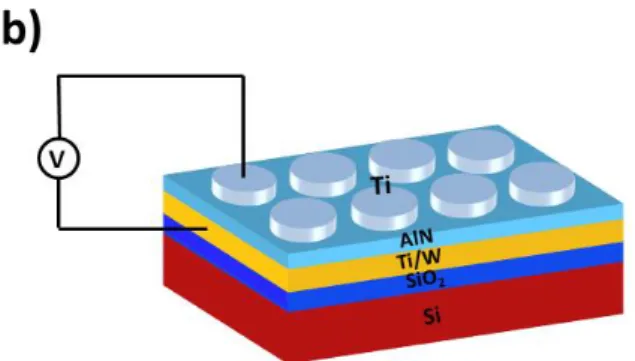
for optoelectronic characterizations. 120-nm-thick Al contact pad and finger layer is formed by thermal evaporation followed by lift-off process. A schematic device structure is shown in the Figure 2.1.
6
2.3 Electrical Characterization
Electrical characterization of ZnO resistive switching device is performed through a direct current voltage (I-V) measurement in a double sweeping mode by using Agilent B1500A semiconductor parameter analyzer. Initially, the virgin device allows a very low amount of current, which is less than 100µA/cm2. In order to observe resistive switching, a controlled breakdown process, called electroforming, is required. During this process, device undergoes atomic scale modifications as a result of high electrical bias and a current compliance is required to prevent permanent damage due to excess current flow. Conductive paths, called filaments, are formed inside the ZnO layer via electric field induced redox reactions [33] and Joule heating [34] enhancing zinc and oxygen ion migration; resulting in an abrupt increase in the overall conductivity of the films.
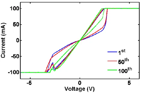
Electroforming process is performed by applying voltage bias of -6V for 1 second with a current compliance of 100mA. The resistive switching behavior of the devices, achieved by varying voltage bias between -6 and 6V in double sweep mode, with the same current compliance is shown in the Figure 3.2a. Starting with high resistance state (HRS), the device remains in this state during the voltage sweep from -6 to 6V until it reaches about a set voltage (Vset) of
2.4V. At this point, the amplitude of the current sharply rises to the limit value and the device switches to low resistance state (LRS) via set process. As the voltage is swept from 6 to -6V for a device initially at LRS, an abrupt decrease in the current amplitude occurs at around -2.4V (Vreset) and the device switches
back to HRS. The device exhibits more than 100 repeated switching cycles between HRS and LRS. During these cycles, the device exhibits excellent stability since the set and reset voltages vary less than 0.3V and the hysteresis curve does not change significantly. The RHRS/RLRS contrast ratio is 3, which is a
7
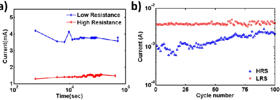
Figure 2.2 Hysteretic resistive switching behavior of Al/ZnO/Si device Retention times more than 5 days have been observed for the device at both states as shown in the Figure 2.3 (a). The states of the devices are read with 0.1V bias at each 60s continuously for one day and then measured consecutively a week after in a room temperature environment. The readout voltage is found to be nondestructive. Devices maintain their states HRS and LRS individually and reach retention times more than 105 seconds without an external electrical power, indicating that the memory device is nonvolatile and stable at room temperature.
An endurance test of the device is performed by the cyclic switching operation. Figure 2.3 (b) shows the two well-resolved states in 100 cycles. The current values were read out at 0.1V for each DC sweep. The RHRS/RLRS contrast ratio is
larger than 3, which is a low contrast ratio for a resistive switching device. Although, current value has some fluctuation, after around the 45th cycle degradation in the RHRS/RLRS contrast ratio is observed.
8
Figure 2.3 a) Retention time measurements at room temperature and b) Endurance test of ZnO resistive switching memory device
2.3 TEM and EDX Characterization
To have a better understanding of the origins of the resistive switching mechanism of the Al/ZnO/Si device, HRTEM, EFTEM and EDX analyses are performed.
To prepare TEM samples, three virgin devices are configured to different resistance states: virgin, HRS and LRS. TEM samples are prepared by taking cross-sectional slices from an active device area with fingers. The HRS and LRS devices are prepared after several time cycling operations. Sample preparation is performed using FEI Nova 600i Nanolab Focused Ion Beam (FIB) Milling device by etching with Ga ions. The thicknesses of the samples are less than 100-nm. To prevent Ga ion damage, Ga ion beams of small voltage, small current and small angle are used. ZnO films retain its polycrystalline structure and Si substrate is still in single crystalline form as evident in the TEM images. Also the EDX data did not reveal the presence of Ga ion, so Ga ion damage is not an issue in our experiment.
9
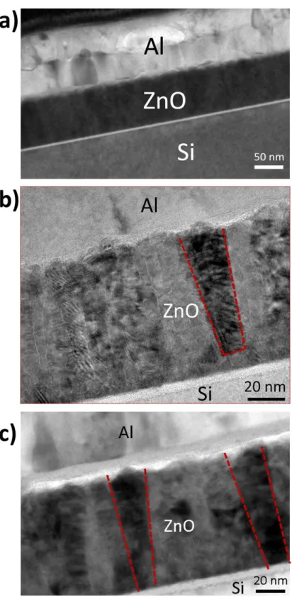
The HRTEM images of the devices (virgin, HRS and LRS) are shown in Figure 2.4. Initially, for virgin devices the ZnO film is in polycrystalline form. After the electroforming process, conductive filaments are formed via electric field induced redox reactions [33] and Joule heating [34] enhanced zinc and oxygen ion migration; resulting in an increase in the overall conductivity of the films. This process is irreversible; the conductive filaments cannot completely dissolve after applying an opposite polarity voltage and the device cannot return to its virgin state. In many transition metal oxides, oxygen ion defects and oxygen vacancies are much more mobile than cations under an external electric field [26, 35]. Migration of oxygen ions via electric field cause the oxygen vacancy doping, resulting in a steady decrease of the resistance. The HRTEM image of the LRS device shown in the Figure 2.4 (c) depicts conducting filaments reaching from the top electrode to the bottom Si substrate. When the switching is OFF, partial ruptures of the conductive filaments are observed via Joule heating by reverse direction. The HRTEM image of the HRS device in Figure 2.4 (b) depicts partially dissolved filaments contributing to decrease in the conduction current while a considerable amount of fully conducting filaments exists. The remaining conducting paths prevent the whole ZnO layer to behave like a good insulator; therefore, a relatively low contrast ratio of 3 is achieved between two resistance states (RHRS/RLRS).
10
Figure 2.4 Cross sectional HRTEM image of a) virgin b) HRS and c) LRS devices
11
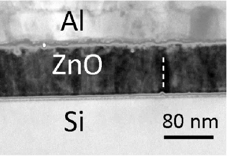
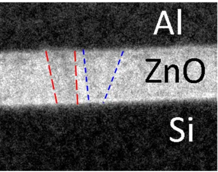
In order to understand the transition between HRS and LRS, EDX measurements of the filamentary and bulk region are performed. Our EDX system gives the elemental presence along with the atomic concentration. The EDX measurements were taken along a line as shown in Figure 2.5.
Figure 2.5 A representative TEM image that verifies the region of EDX measurement along the line
Table 2.1 The atomic percentage of Zn and O within a filamentary and bulk regions for HRS and LRS.
We took four different measurements, within a filamentary and no filamentary (bulk) region for HRS and LRS. We compared the Zn and O ratio of the LRS and HRS devices within a filamentary and no filamentary (bulk) region. The atomic percentage of Zn is higher than that of O in filamentary region and to compare the HRS and LRS, Zn percentage is higher in LRS as given in Table
Filamentary Region Bulk Region
Atomic Percentage Zn (%) O (%) Zn (%) O (%)
HR State 52.18 47.82 50.20 49.80
12
2.1. The percentage values are calculated as the average atomic percentage of each atom on every measurement point along the line.
In addition, EFTEM image demonstrating oxygen concentrations in Figure 2.6 shows lower oxygen concentration within a filament region compared to bulk regions and supports the stoichiometric change within ZnO films.
Figure 2.6 EFTEM image showing the oxygen deficiency within a filamentary region compared to bulk region
2.4 Conclusion
In conclusion, resistive switching behavior of Al/ZnO/Si device is related with the conductive filament formation and dissolution during voltage application. When the virgin device is changed the initially highly insulating state to activate the resistive switching, the overall resistance of the film decreased approximately 106 times due to the filament formation via redox reduction and Joule heating. The formation and rupture of the filamentary regions are observed
13
via TEM images. EDX and EFTEM results show the variation in oxygen concentration within a filamentary region, resulting the switching between HRS and LRS. A low contrast ratio of 3 is achieved between two resistance states is due to the non-dissolved filaments at HRS. The device shows non-volatile bipolar resistive switching behavior over cycling.
14
Chapter 3
Resistive
Switching
Behavior
of
HCPA-ALD Grown AlN
3.1 Introduction
Resistive switching characteristics of almost all anion based transition metal oxides are studied intensely. However, non-oxide ionic insulators and semiconductors are not extensively reported. Resistive switching property of AlN [22, 36-38] films is explored in a few works. However, the self-compliance current behavior of AlN resistive switching devices has not shown before. Generally, to activate resistive switching property, a controlled, non-reversible breakdown process, which is called electroforming, achieved by applying high voltages is required [33]. A current limiting circuit is essential to protect the device from permanent damage and to increase endurance of the device. To build up a current compliance element, such as transistor and diode, has been regarded an important issue to commercialize resistive switching memories. The
15
self-compliance effect is helpful for memory circuit design in terms of reducing the complexity of the circuit. Moreover, resistive switching devices can be scaled down to 10nm [15], however, additional current compliance elements restrict the scalability of this memory system.
In this work, we successfully investigated the bipolar resistive switching characteristic of AlN films with a self-compliance of current property. AlN films were deposited using hollow cathode plasma assisted atomic layer deposition (HCPA-ALD) technique.
3.2 Device Fabrication
Figure 3.1 (a) A cross sectional TEM image (b) Schematic illustration of device structure
AlN resistive switching memories are fabricated on a thermally grown 1µm-thick SiO2 on Si substrate. As a bottom electrode, a 100nm Ti/W metal alloy is
sputtered with DC magnetron sputtering of a Ti/W (10:90) target. A 10-12 nm AlN thin film is deposited with a hollow cathode plasma assisted atomic layer deposition (HCPA-ALD) system using trimethylaluminium (TMA, Al(CH3)3) and N2:H2 (50:50 SCCM) gas mixture at a wafer temperature of 200°C. Finally,
a 100nm Ti top electrode is deposited by sputtering through a shadow mask to complete device fabrication. A cross sectional TEM image of the device is
16
shown in Figure 3.1 (a) and a representative device structure is shown in Figure 3.1 (b).
3.3 Device Characterization
3.2.1 AlN Material Characterization
Our group has optimized the deposition of AlN films by using a modified Fiji F200-LL ALD reactor (Ultratech/Cambridge NanoTech Inc.), which is pumped by an Edward NXDS20iC dry scroll vacuum pump [39]. This system is modified by replacing its original quartz-based plasma source with a stainless steel hollow cathode plasma (HCP) source (Meaglow Ltd.). The optimized AlN films are deposited at a wafer temperature of 200°C using trimethylaluminium (TMA, Al(CH3)3) and N2:H2 (50:50 SCCM) gas mixture. The optimized growth
per cycle (GPC) value is 0.99°A and the refractive index (n) of the film is 1.94. AlN films with wafer level non-uniformities less than ±1.5% are achieved. GIXRD patterns of AlN films exhibit hexagonal (wurtzite) polycrystalline structure with crystallite sizes of 19.2 and 24.8 nm. (See Figure 10 (a)) XPS survey analyses showed 2.5-3.0 %O and no C impurities in AlN films, after etching in situ with a beam of Ar ions under UHV conditions. (See Figure 6)
3.2.1 AlN Resistive Switching Memory Characteristics
Electrical characterization of the AlN resistive switching device is performed through a direct current (DC) voltage (I-V) measurement in a double sweeping mode by using Keithley 4200 semiconductor parameter analyzer. Voltage bias is applied from the Ti top electrode while keeping bottom Ti-W electrode grounded. The virgin device passes a very low amount of current, on the order
17
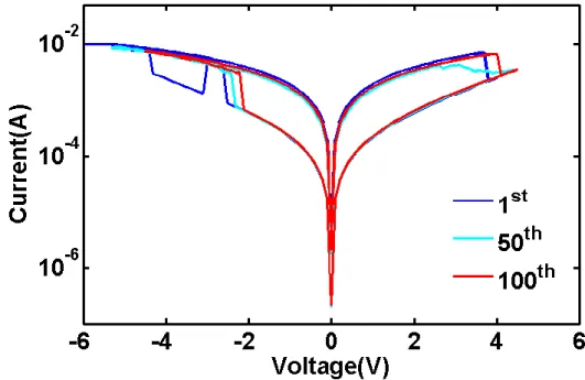
of 10-9A. In order to activate resistive switching a controlled but irreversible breakdown process is applied. Electroforming process is performed by varying voltage from 0 to 6 V. Around 5.4 V a sudden increase in the current value which is on the order of 10-6 A is observed. During this process, device undergoes atomic scale modifications and conductive filaments are formed. Figure 3.2 shows the hysteretic current versus voltage (I-V) characteristic of an AlN resistive switching device in a semi-logarithmic scale with Vset voltages
ranging between -2 to -5V and Vreset voltages ranging between 4 to 6V. Starting
with a HRS, the device remains in this state until it reaches a Vset value. At this
point system set to a LRS with an abrupt increase in current. As the voltage is swept back to the starting value, the abrupt decrease in current occurs at a Vreset
voltage value and the device is reset back to the LRS. The device shows a self-compliance of current flowing, resulting in high endurance over cycling.
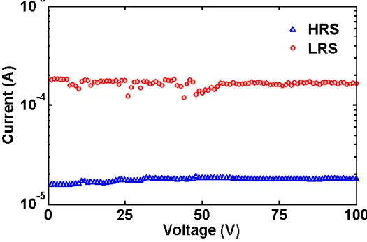
Figure 3.2 Hysteretic resistive switching behavior of Ti/AlN/Ti-W device An endurance test of the device is performed by the cyclic switching operation. Figure 3.2 shows the HRS and LRS as well-resolved in 100 cycles. The current values were read out at 0.1V for each DC sweep. Although, current value has
18
some fluctuation, no significant degradation in the RHRS/RLRS contrast ratio is
observed.
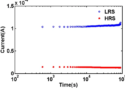
Figure 3.3 The current of HRS and LRS vs the number of switching cycles at 0.1 V readout voltage.
The nonvolatile memory characteristic of the device is examined in Figure 3.4. Retention times more than 105 seconds have been observed for the device at both HRS and LRS. The states of the devices are read with 0.1V bias at every 60s continuously in a room temperature environment. The readout voltage is found to be nondestructive. Devices maintain their states HRS and LRS individually and reach retention times more than 105 seconds without an external electrical power, indicating that the memory device is nonvolatile and stable at room temperature.
19
Figure 3.4 Stability of both HRS and LRS at room temperature
Many models of carrier transport mechanism for resistive switching devices have been reported by previous works. These models include space charge limited current (SCLC), Schottky emission, Poole-Frenkel emission and Fowler-Nordheim quantum tunneling. These models can be identified in terms of I-V curves. The linear IαV indicates Ohmic [40], exponential in IαV indicates Poole Frenkel [41] or Fowler-Nordheim emission [42] , and IαV2 indicates SCLC [29]. In order to have a better understanding of the conduction mechanism of the Ti/AlN/Ti-W resistive switching device, the I-V data is plotted on a log-log scale as shown in Figure 3.5.
The slope of the I-V curve in the logarithmic scale graph shows a linear relationship between voltage and current at LRS indicating that the conduction mechanism for LRS is ohmic for both negative and positive voltage values. The conduction mechanism of the HRS is also ohmic at low voltages, while a space charge limited conduction (SCLC) mechanism is observed at increased applied voltages. The combined ohmic and SCLC mechanisms together indicate that the resistive switching mechanism is due to the formation and rupture of conducting filaments in the AlN layer [43].
20
Figure 3.5 I-V curves in a double logarithmic scale for a) positive voltage and b) negative voltage values
3.4 Conclusion
Resistive switching characteristics of HCPE-ALD grown AlN films are investigated. As deposited AlN thin films are verified to exhibit stoichiometric hexagonal polycrystalline structure with less than 3% oxygen and carbon
21
impurities. The Ti/AlN/Ti-W device shows a bipolar resistive switching behavior with a self-compliance of current. Reversible, nonvolatile and reproducible resistive switching characterizations successfully demonstrated. The resistive switching mechanism is mainly ascribed to the formation and dissolution of conductive filaments.
22
Chapter 4
Optoelectronic Applications of
Resistive Switching
4.1 Introduction
Today’s active light engineering technologies are mainly based on the optical modulators. Optical modulation is heavily used for integrated optical interconnects to solve the interconnect bottleneck in complementary metal oxide semiconductor (CMOS) technology, however recent innovations in photonics expanded its applications in imaging [44], active matrix displays [45], bio-sensing [46], telecommunications [47], radio frequency and terahertz applications [48]. Conventional optical modulators are achieved by using plasma dispersion [49] via electrical modulation of free carrier concentration in semiconductors. However, fast [19], energy efficient [18], compact [35], scalable and integrable [20] modulation technologies are required for new applications.
23
In this chapter, resistive switching is introduced as an alternative method to modulate light by exploiting atomic scale modifications using electrical stimuli. The resistive switching memory explained in chapter 2 is used for optical modulation demonstration. The optical modulation mechanism is modeled by the modulation of effective doping concentration in the ZnO active layer. Up to 2 orders of magnitude modulation in effective doping concentration inside the active layer is predicted by our theoretical model.
4.2 Device Characterization
In chapter 2, resistive switching memory characterization and its TEM and EDX results were explained in detail. In order to investigate the effect of resistive switching on the optical characteristics of the device are performed via reflection measurements using a fourier transform infrared spectrometer (FTIR) from the finger part of the device represented in the Figure 2.1b while the device is electrically biased using the top contact pad and the bottom electrode. Reflection measurements are performed using Bruker Vertex 70 Fourier Transform Infrared Spectrometer with Hyperion 2000 Microscope attachment. The size of the FTIR probe beam is ca 250250μm2, smaller than the device area. The FTIR system is coupled with a Keithley 2400 source measure unit and the optical measurements are observed simultaneously. The hysteretic behavior is observed in the reflection spectrum vs applied voltage bias. Figure 4.1 shows a representative hysteretic behavior of reflection at 8µm wavelength as a function of voltage bias. The highest contrast of reflection between low resistance and high resistance state is observed at 8µm. Applying voltage from 0 to 6V at LRS, the change in the reflection is below 1% until a bias voltage value of 6V. Right after 4V of bias, a sudden drop in the reflection by 4% is observed. Applying voltage back from 6 to 0V, reflection does not change significantly at HRS. To keep looping from 0 to 6V, reflection spectrum goes into a steady increase towards its original value at LRS. The reflection-voltage loop and
24
current voltage loop does not correlate in terms of Vset and Vreset voltages.
Because to observe the state transition in the electrical I-V measurements, formation and dissolution of the tip of some of the filaments is sufficient. Further atomic reorganization within the rest of the film results in a more global change that is observed as optical state transition. When the voltage bias is removed, the programmed optical reflection state (LRS or HRS) remains same, so the effect is verified as non-volatile. Therefore, the resulting modulation in the reflection spectra is attributed to the change in the optical constants of ZnO layer due to atomic scale modifications caused by resistive switching.
Figure 4.1 Reflection loop at the wavelength of 8µm as a function of bias voltage
An ultra-broadband non-volatile modulation in the reflection within 5-18µm spectrum by 4% is observed at 0V between HRS and LRS in Figure 4.2.
Low Resistance
25
Figure 4.2 A non-volatile modulation of reflection by 4% in the 5-18µm FTIR reflection spectrum, measured at 0V
In order to further investigate the effect, capacitance voltage measurements are utilized as shown in Figure 4.3. A cyclic voltage bias between -6 and 6V resulted in non-volatile hysteretic capacitance values. In addition, capacitance value of a two terminal device is known to be quite sensitive to localized morphological changes within the active layer as opposed to its resistance value [50]. Especially, variation in the dielectric parameters would reflect on the measured device capacitance. We apply a DC voltage sweep, the same as the I-V measurement. At integer values of voltage, we perform impedance-frequency measurement, and extract the capacitance value at 20 kHz. We use a very small AC voltage to make sure the device state is not disturbed. The switching occurs at the usual set/reset voltage for resistive switching. Resistance measurement shows sudden switching into LRS, for instance, when Zn-rich filament forms a conductive path. When measuring capacitance, on the other hand, a more gradual transition is observed since measured capacitance is not dominated by a localized filament, but rather the effective dielectric medium, where Zn and O atoms are gradually migrating during the switching.
26
Figure 4.3 The hysteritic capacitance of Al/ZnO/Si device as a function of voltage bias
As stated in chapter 2, oxygen concentrations in a filamentary region of the device exhibits lower concentration compared to bulk region. EDX results show a clear contrast in Zn/O ratio within the filamentry regions between LRS and HRS. Difference in the average Zn to O concentration on filamentary regions with respect to non-filamentary regions in terms of signal counts in EDX spectroscopy is measured to be 5% for LRS whereas it is about 1.85% for HRS indicating improved stoichiometry for HRS. For thin film ZnO, zinc interstitials or oxygen vacancies are reported to account for unintentional doping. These findings also support that electro-optical modulation observed in the FTIR measurements are caused by variation of effective doping caused by variation of oxygen concentration inside the filaments between HRS and LRS.
4.4 Conclusion
In conclusion, we demonstrated resistive switching as a new and viable optical modulation technique. By fabricating Al/ZnO/Si structure, we represented a
27
proof-of-principle non-volatile and repeatable optical modulation via resistive switching behavior. Through FTIR reflection measurements, we showed optical modulation of reflection by 4% within the spectral range covering nearly the entire mid and long-wave infrared wavelengths. The performed capacitance measurements indicating variation of dielectric parameters exhibit hysteretic behavior similar to that of the resistive switching characteristics. HRTEM and EDX results support the variation of local stoichiometry within the filamentary regions which supports optical modulation mechanism. The results of this work bridge resistive switching mechanism to optical modulation and enable alternative modulation schemes such as reconfigurable non-volatile surfaces, imagers, emitters as well as electro-optic memories.
28
Chapter 5
Conclusions
Conventional charge based memories will face severe problems when the scaling limit is approached. The development of new non-volatile memories with high performance, power consumed, low cost and fast properties is attracting extreme attention. Therefore, resistive switching memories are potential candidates for future conventional non-volatile memory to overcome the physical and technological limitations and fulfill the essential requirements for 3-D integrated circuit architecture. The resistive switching behavior of almost all transition metal oxides, as well as other insulators/semiconductors such as metal-nitrides, sulfides, fluorides, carbides and phosphides are studied. However the physical mechanisms behind resistive switching still remains uncertain. Several mechanisms were reported such as local capture and dissolution of filaments, ion transport recombination effect, space-charge-limited current (SCLC) trap mechanism and interface effect. Among these models, the formation and capture of filaments is strongly championed via in-situ transmission electron microscopy (TEM) studies.
29
This thesis presents analysis of the switching mechanism of Al/ZnO/Si device. We propose the stoichiometric change due to switching and support via TEM and EDX. We used this device to show resistive switching as a new and viable way of optoelectronic modulation technique. These results pave the way for reconfigurable non-volatile surfaces, imagers, emitters, electro-optic memories. Non-oxide ionic dielectrics also reveal resistive switching behavior, but less has been reported so far. Resistive switching mechanism of nitrides has not been intensely studied. We showed the bipolar resistive switching behavior of AlN films with self-compliance of current. The wide band gap, high electrical resistivity, and high thermal conductivity of AlN make it a good candidate for a resistive switching memory device.
In future, these devices may be used in non-volatile memory, reconfigurable neuromorphic applications and optoelectronic applications.
30
Bibliography
[1] T. Hickmott, "Low‐frequency negative resistance in thin anodic oxide films," Journal of Applied Physics, vol. 33, pp. 2669-2682, 1962.
[2] J. N. Cole, J. J. Cuomo, R. B. Laibowitz, and K. C. Park, "Bistable resistance device which does not require forming," ed: US Patent 3,796,926, 1974.
[3] J. Gibbons and W. Beadle, "Switching properties of thin NiO films,"
Solid-State Electronics, vol. 7, pp. 785-790, 1964.
[4] G. Dearnaley, A. Stoneham, and D. Morgan, "Electrical phenomena in amorphous oxide films," Reports on Progress in Physics, vol. 33, p. 1129, 1970.
[5] D. Frohman‐Bentchkowsky, "Memory behavior in a floating‐gate avalanche‐injection MOS (FAMOS) structure," Applied Physics Letters, vol. 18, pp. 332-334, 1971.
[6] A. Asamitsu, Y. Tomioka, H. Kuwahara, and Y. Tokura, "Current switching of resistive states in magnetoresistive manganites," Nature, vol. 388, pp. 50-52, 1997.
[7] M. Kozicki, M. Yun, L. Hilt, and A. Singh, "Applications of programmable resistance changes in metal-doped chalcogenides,"
Pennington NJ USA: Electrochem. Soc, pp. 298-309, 1999.
[8] A. Beck, J. Bednorz, C. Gerber, C. Rossel, and D. Widmer, "Reproducible switching effect in thin oxide films for memory applications," Applied
Physics Letters, vol. 77, pp. 139-141, 2000.
[9] N. A. Melosh, A. Boukai, F. Diana, B. Gerardot, A. Badolato, P. M. Petroff, and J. R. Heath, "Ultrahigh-density nanowire lattices and circuits,"
Science, vol. 300, pp. 112-115, 2003.
[10] Ö. Türel and K. Likharev, "CrossNets: Possible neuromorphic networks based on nanoscale components," International journal of circuit theory
and applications, vol. 31, pp. 37-53, 2003.
[11] J. R. Heath, P. J. Kuekes, G. S. Snider, and R. S. Williams, "A defect-tolerant computer architecture: Opportunities for nanotechnology,"
31
[12] D. B. Strukov and K. K. Likharev, "Prospects for terabit-scale nanoelectronic memories," Nanotechnology, vol. 16, p. 137, 2005.
[13] W. Zhuang, W. Pan, B. Ulrich, J. Lee, L. Stecker, A. Burmaster, D. Evans, S. Hsu, M. Tajiri, and A. Shimaoka, "Novel colossal magnetoresistive thin film nonvolatile resistance random access memory (RRAM)," in Electron
Devices Meeting, 2002. IEDM'02. International, 2002, pp. 193-196.
[14] I. Baek, M. Lee, S. Seo, M.-J. Lee, D. Seo, D.-S. Suh, J. Park, S. Park, T. Kim, and I. Yoo, "Highly scalable nonvolatile resistive memory using simple binary oxide driven by asymmetric unipolar voltage pulses," in
Electron Devices Meeting, 2004. IEDM Technical Digest. IEEE International, 2004, pp. 587-590.
[15] K. Szot, W. Speier, G. Bihlmayer, and R. Waser, "Switching the electrical resistance of individual dislocations in single-crystalline SrTiO3," Nature
materials, vol. 5, pp. 312-320, 2006.
[16] "Emerging Research Devices" tech. rep, International Technology Roadmap for Semiconductors, 2009.
[17] A. Geresdi, M. Csontos, A. Gubicza, A. Halbritter, and G. Mihály, "A fast operation of nanometer-scale metallic memristors: highly transparent conductance channels in Ag2S devices," Nanoscale, vol. 6, pp. 2613-2617,
2014.
[18] H.-Y. Lee, P.-S. Chen, C.-C. Wang, S. Maikap, P.-J. Tzeng, C.-H. Lin, L.-S. Lee, and M.-J. Tsai, "Low-power switching of nonvolatile resistive memory using hafnium oxide," Japanese journal of applied physics, vol. 46, p. 2175, 2007.
[19] Y. C. Yang, F. Pan, Q. Liu, M. Liu, and F. Zeng, "Fully room-temperature-fabricated nonvolatile resistive memory for ultrafast and high-density memory application," Nano letters, vol. 9, pp. 1636-1643, 2009. [20] S. H. Jo and W. Lu, "CMOS compatible nanoscale nonvolatile resistance
switching memory," Nano letters, vol. 8, pp. 392-397, 2008.
[21] S. Yu, H.-Y. Chen, B. Gao, J. Kang, and H.-S. P. Wong, "HfOx-based
vertical resistive switching random access memory suitable for bit-cost-effective three-dimensional cross-point architecture," ACS nano, vol. 7, pp. 2320-2325, 2013.
[22] B. J. Choi, J. J. Yang, M.-X. Zhang, K. J. Norris, D. A. Ohlberg, N. P. Kobayashi, G. Medeiros-Ribeiro, and R. S. Williams, "Nitride memristors," Applied Physics A, vol. 109, pp. 1-4, 2012.
32
[23] B. F. Bory, H. L. Gomes, R. A. Janssen, D. M. de Leeuw, and S. C. Meskers, "Role of Hole Injection in Electroforming of LiF-Polymer Memory Diodes," The Journal of Physical Chemistry C, vol. 116, pp. 12443-12447, 2012.
[24] W. Lee, J. Park, M. Son, J. Lee, S. Jung, S. Kim, S. Park, J. Shin, and H. Hwang, "Excellent state stability of Cu/SiC/Pt programmable metallization cells for nonvolatile memory applications," Electron Device
Letters, IEEE, vol. 32, pp. 680-682, 2011.
[25] S. Balasubramanian, V. Kumar, N. Balasubramanian, and V. Premachandran, "Resistance switching in indium phosphide using hydrogen passivation of acceptors," Applied Physics Letters, vol. 64, pp. 2256-2257, 1994.
[26] J. J. Yang, D. B. Strukov, and D. R. Stewart, "Memristive devices for computing," Nature nanotechnology, vol. 8, pp. 13-24, 2013.
[27] D.-H. Kwon, K. M. Kim, J. H. Jang, J. M. Jeon, M. H. Lee, G. H. Kim, X.-S. Li, G.-X.-S. Park, B. Lee, and X.-S. Han, "Atomic structure of conducting nanofilaments in TiO2 resistive switching memory," Nature
nanotechnology, vol. 5, pp. 148-153, 2010.
[28] B. Gao, J. Kang, L. Liu, X. Liu, and B. Yu, "A physical model for bipolar oxide-based resistive switching memory based on ion-transport-recombination effect," Applied Physics Letters, vol. 98, p. 232108, 2011. [29] Y. Xia, W. He, L. Chen, X. Meng, and Z. Liu, "Field-induced resistive
switching based on space-charge-limited current," Applied Physics Letters, vol. 90, pp. 022907-022907-3, 2007.
[30] H. Hwang, Y. Iwasa, M. Kawasaki, B. Keimer, N. Nagaosa, and Y. Tokura, "Emergent phenomena at oxide interfaces," Nature materials, vol. 11, pp. 103-113, 2012.
[31] J.-Y. Chen, C.-L. Hsin, C.-W. Huang, C.-H. Chiu, Y.-T. Huang, S.-J. Lin, W.-W. Wu, and L.-J. Chen, "Dynamic evolution of conducting nanofilament in resistive switching memories," Nano letters, vol. 13, pp. 3671-3677, 2013.
[32] Y. Yang, P. Gao, S. Gaba, T. Chang, X. Pan, and W. Lu, "Observation of conducting filament growth in nanoscale resistive memories," Nature
communications, vol. 3, p. 732, 2012.
[33] R. Waser, R. Dittmann, G. Staikov, and K. Szot, "Redox‐Based Resistive Switching Memories–Nanoionic Mechanisms, Prospects, and Challenges,"
33
[34] U. Russo, D. Ielmini, C. Cagli, and A. L. Lacaita, "Self-accelerated thermal dissolution model for reset programming in unipolar resistive-switching memory (RRAM) devices," Electron Devices, IEEE
Transactions on, vol. 56, pp. 193-200, 2009.
[35] R. Waser and M. Aono, "Nanoionics-based resistive switching memories,"
Nature materials, vol. 6, pp. 833-840, 2007.
[36] C. Chen, Y. Yang, F. Zeng, and F. Pan, "Bipolar resistive switching in Cu/AlN/Pt nonvolatile memory device," Applied Physics Letters, vol. 97, pp. 083502-083502-3, 2010.
[37] H.-D. Kim, H.-M. An, Y. Seo, and T. Geun Kim, "Transparent resistive switching memory using ITO/AlN/ITO capacitors," Electron Device
Letters, IEEE, vol. 32, pp. 1125-1127, 2011.
[38] H.-D. Kim, H.-M. An, E. B. Lee, and T. G. Kim, "Stable bipolar resistive switching characteristics and resistive switching mechanisms observed in aluminum nitride-based ReRAM devices," Electron Devices, IEEE
Transactions on, vol. 58, pp. 3566-3573, 2011.
[39] C. Ozgit-Akgun, E. Goldenberg, A. K. Okyay, and N. Biyikli, "Hollow cathode plasma-assisted atomic layer deposition of crystalline AlN, GaN and AlxGa1−xN thin films at low temperatures," Journal of Materials
Chemistry C, vol. 2, pp. 2123-2136, 2014.
[40] P. A. Leighton, "Electronic Processes in Ionic Crystals (Mott, N. F.; Gurney, R. W.)," Journal of Chemical Education, vol. 18, p. 249, 1941/05/01 1941.
[41] J. Yeargan and H. Taylor, "The Poole‐Frenkel Effect with Compensation Present," Journal of Applied Physics, vol. 39, pp. 5600-5604, 1968.
[42] Y. Watanabe, "Electrical transport through Pb(Zr,Ti)O3 pn and pp
heterostructures modulated by bound charges at a ferroelectric surface: Ferroelectric pn diode," Physical Review B, vol. 59, p. 11257, 1999.
[43] K. M. Kim, B. J. Choi, Y. C. Shin, S. Choi, and C. Seong Hwang, "Anode-interface localized filamentary mechanism in resistive switching of TiO2
thin films," Applied Physics Letters, vol. 91, pp. 012907-012907-3, 2007. [44] A. Garcia Sega, B. H. King, J. Y. Lee, M. J. Sailor, and G. M. Miskelly,
"Thermally Modulated Porous Silica Multispectral Filters and Their Application in Remote Imaging," ACS nano, vol. 7, pp. 7785-7794, 2013. [45] D. Fattal, Z. Peng, T. Tran, S. Vo, M. Fiorentino, J. Brug, and R. G.
Beausoleil, "A multi-directional backlight for a wide-angle, glasses-free three-dimensional display," Nature, vol. 495, pp. 348-351, 2013.
34
[46] H. Kang, C.-J. Heo, H. C. Jeon, S. Y. Lee, and S.-M. Yang, "Durable Plasmonic Cap Arrays on Flexible Substrate with Real-Time Optical Tunability for High-Fidelity SERS Devices," ACS applied materials &
interfaces, vol. 5, pp. 4569-4574, 2013.
[47] G. T. Reed, G. Mashanovich, F. Gardes, and D. Thomson, "Silicon optical modulators," Nature photonics, vol. 4, pp. 518-526, 2010.
[48] B. Sensale-Rodriguez, R. Yan, M. M. Kelly, T. Fang, K. Tahy, W. S. Hwang, D. Jena, L. Liu, and H. G. Xing, "Broadband graphene terahertz modulators enabled by intraband transitions," Nature communications, vol. 3, p. 780, 2012.
[49] R. A. Soref and B. R. Bennett, "Electrooptical effects in silicon," Quantum
Electronics, IEEE Journal of, vol. 23, pp. 123-129, 1987.
[50] C. Van Opdorp, "Evaluation of doping profiles from capacitance measurements," Solid-State Electronics, vol. 11, pp. 397-406, 1968.