Microstructured porous ZnO thin film for
increased light scattering and improved
efficiency in inverted organic photovoltaics
Amoolya Nirmal,1 Aung Ko Ko Kyaw,2,6 Xiao Wei Sun 1,5 and Hilmi Volkan Demir1,3,4* 1LUMINOUS! Center of Excellence for Semiconductor Lighting and Displays, School of Electrical and Electronic
Engineering, Nanyang Technological University, Nanyang Avenue, 639798, Singapore 2 Institute of Materials Research and Engineering, Agency for Science Technology and Research (A*STAR),
Singapore 117602, Singapore
3School of Physical and Mathematical Sciences, Nanyang Technological University, Nanyang Avenue, 639798 Singapore
4Department of Electrical and Electronics Engineering, Department of Physics, UNAM-National Nanotechnology Research Center, Bilkent University, Bilkent, Ankara 06800, Turkey
5[email protected] 6[email protected]
Abstract: Microstructured porous zinc oxide (ZnO) thin film was
developed and demonstrated as an electron selective layer for enhancing light scattering and efficiency in inverted organic photovoltaics. High degree of porosity was induced and controlled in the ZnO layer by incorporation of polyethylene glycol (PEG) organic template. Scanning electron microscopy, contact angle and absorption measurements prove that the ZnO:PEG ratio of 4:1 is optimal for the best performance of porous ZnO. Ensuring sufficient pore-filling, the use of porous ZnO leads to a marked improvement in device performance compared to non-porous ZnO, with 35% increase in current density and 30% increase in efficiency. Haze factor studies indicate that the performance improvement can be primarily attributed to the improved light scattering enabled by such a highly porous structure.
©2014 Optical Society of America
OCIS codes: (310.0310) Thin films; (250.0250) Optoelectronics. References and links
1. S. R. Forrest, “The limits to organic photovoltaic cell efficiency,” MRS Bull. 30(01), 28–32 (2005). 2. M. T. Dang, G. Wantz, H. Bejbouji, M. Urien, O. J. Dautel, L. Vignau, and L. Hirsch, “Polymeric solar cells
based on P3HT:PCBM: Role of the casting solvent,” Sol. Energy Mater. Sol. Cells 95(12), 3408–3418 (2011). 3. J. D. Servaites, M. A. Ratner, and T. J. Marks, “Organic solar cells: A new look at traditional models,” Energy &
Environmental Science 4(11), 4410–4422 (2011).
4. V. Shrotriya, L. Gang, Y. Yan, T. Moriarty, K. Emery, and Y. Yang, “Accurate measurement and characterization of organic solar cells,” Adv. Funct. Mater. 16(15), 2016–2023 (2006).
5. C. W. Tang, “Two-layer organic photovoltaic cell,” Appl. Phys. Lett. 48(2), 183–185 (1986).
6. Z. He, C. Zhong, S. Su, M. Xu, H. Wu, and Y. Cao, “Enhanced power-conversion efficiency in polymer solar cells using an inverted device structure,” Nat. Photonics 6(9), 593–595 (2012).
7. “http://www.heliatek.com/”, retrieved.
8. Y. Yao, J. Hou, Z. Xu, G. Li, and Y. Yang, “Effects of solvent mixtures on the nanoscale phase separation in polymer solar cells,” Adv. Funct. Mater. 18(12), 1783–1789 (2008).
9. X. W. Sun, D. W. Zhao, L. Ke, A. K. K. Kyaw, G. Q. Lo, and D. L. Kwong, “Inverted tandem organic solar cells with a MoO3/Ag/Al/Ca intermediate layer,” Appl. Phys. Lett. 97(5), 053303 (2010).
10. S. H. Park, A. Roy, S. Beaupre, S. Cho, N. Coates, J. S. Moon, D. Moses, M. Leclerc, K. Lee, and A. J. Heeger, “Bulk heterojunction solar cells with internal quantum efficiency approaching 100%,” Nat. Photonics 3(5), 297– 302 (2009).
12. A. K. K. Kyaw, X. W. Sun, C. Y. Jiang, G. Q. Lo, D. W. Zhao, and D. L. Kwong, “An inverted organic solar cell employing a sol-gel derived ZnO electron selective layer and thermal evaporated MoO3 hole selective layer,” Appl. Phys. Lett. 93(22), 221107 (2008).
13. K. Takanezawa, K. Tajima, and K. Hashimoto, “Efficiency enhancement of polymer photovoltaic devices hybridized with ZnO nanorod arrays by the introduction of a vanadium oxide buffer layer,” Appl. Phys. Lett. 93(6), 063308 (2008).
14. K. X. Steirer, J. P. Chesin, N. E. Widjonarko, J. J. Berry, A. Miedaner, D. S. Ginley, and D. C. Olson, “Solution deposited NiO thin-films as hole transport layers in organic photovoltaics,” Org. Electron. 11(8), 1414–1418 (2010).
15. Z. Y. Hu, J. J. Zhang, Y. Liu, Y. N. Li, X. D. Zhang, and Y. Zhao, “Efficiency enhancement of inverted organic photovoltaic devices with ZnO nanopillars fabricated on FTO glass substrates,” Synth. Met. 161(19-20), 2174– 2178 (2011).
16. Z. F. Liu, Z. G. Jin, W. Li, and J. J. Qiu, “Preparation of ZnO porous thin films by sol-gel method using PEG template,” Mater. Lett. 59(28), 3620–3625 (2005).
17. X. H. Ju, W. Feng, K. C. Varutt, T. S. Hori, A. H. Fujii, and M. N. Ozaki, “Fabrication of oriented ZnO nanopillar self-assemblies and their application for photovoltaic devices,” Nanotechnology 19(43), 435706 (2008).
18. D. A. Rider, R. T. Tucker, B. J. Worfolk, K. M. Krause, A. Lalany, M. J. Brett, J. M. Buriak, and K. D. Harris, “Indium tin oxide nanopillar electrodes in polymer/fullerene solar cells,” Nanotechnology 22(8), 085706 (2011). 19. D. C. Olson, L. Yun-Ju, M. S. White, N. Kopidakis, S. E. Shaheen, D. S. Ginley, J. A. Voigt, and J. W. P. Hsu,
“Effect of polymer processing on the performance of poly(3-hexylthiophene)/ZnO nanorod photovoltaic devices,” J. Phys. Chem. C 111(44), 16640–16645 (2007).
20. K. Takanezawa, K. Hirota, Q. S. Wei, K. Tajima, and K. Hashimoto, “Efficient charge collection with ZnO nanorod array in hybrid photovoltaic devices,” J. Phys. Chem. C 111(19), 7218–7223 (2007).
21. J. Bouclé, H. J. Snaith, and N. C. Greenham, “Simple Approach to Hybrid Polymer/Porous Metal Oxide Solar Cells from Solution-Processed ZnO Nanocrystals,” J. Phys. Chem. C 114(8), 3664–3674 (2010).
22. S. B. Jo, J. H. Lee, M. Sim, M. Kim, J. H. Park, Y. S. Choi, Y. Kim, S.-G. Ihn, and K. Cho, “High performance organic photovoltaic cells using polymer-hybridized ZnO nanocrystals as a cathode interlayer,” Advanced Energy Materials 1(4), 690–698 (2011).
23. Y.-M. Chang and C.-Y. Leu, “Solvent extraction induced nano-porous zinc oxide as an electron transport layer for inverted polymer solar cells,” Org. Electron. 13(12), 2991–2996 (2012).
24. Y. S. Hsiao, C. P. Chen, C. H. Chao, and W. T. Whang, “All-solution-processed inverted polymer solar cells on granular surface-nickelized polyimide,” Org. Electron. 10(4), 551–561 (2009).
1. Introduction
Organic photovoltaics (OPV) promises an alternative, low-cost, green approach to harvest solar energy with advantages of solution processing, ease of fabrication and capability to be deposited on flexible substrates [1–4]. Since the first demonstration of organic donor/acceptor heterojunction by Tang in 1986 [5], there have been tremendous research efforts invested in the OPVs. The highest efficiency reported to date is ~9.2% for a single cell [6] and 12% for a tandem cell [7]. However, the efficiency is still low compared to inorganic solar cells. For low-cost, large-scale deployment of organic photovoltaics, an efficiency level of ~15% should be achieved for commercialization [3]. With the aim of achieving this target several approaches are being employed including the use of additives and mixed solvents, new structures, low bandgap polymers and tandem cells [8–11]. Another possible direction for efficiency enhancement is the use of metal oxides, which serve as an anode or a cathode interfacial layer in OPVs.
Metal oxides offer dual roles for the operation of OPVs. They improve charge extraction by lowering the barrier height at the electrode while blocking the opposite charge from reaching the electrode, thus reducing recombination [3]. A p-type (or p-type like) metal oxide acts as a hole transport layer and electron blocking layer while n-type metal oxide acts as an electron transport layer and a hole blocking layer, thus boosting the device performance. In the case of inverted OPVs, thin layers of p-type metal oxides such as MoO3, V2O5, WO3 and
NiO are used in the place of PEDOT:PSS [12–14]. These oxides exhibit high work functions, good hole conductivity and electron blocking capability, and are usually deposited using thermal evaporation [12]. For electron transport layer, n-type metal oxides such as TiO2 and
ZnO are used. ZnO has high electron mobility as well as high optical transparency in the visible region. Hence, ZnO is a strong candidate for an electron transport layer in inverted
OPVs [15]. Though there are different methods including chemical vapor deposition and spray pyrolysis for depositing ZnO, spin-coating ZnO from the sol-gel is a highly preferred method because of its low cost, composition controllability and the ability to make homogenous films [16].
In comparison with uniform featureless layers, nanostructured metal oxides can enhance the device performance in three ways: increasing the interfacial area between the metal oxide and the active layer, providing better charge collection and stronger light trapping for enhanced optical absorption [17, 18]. These have been demonstrated and well documented using ZnO nanopillar and nanorod structures in inverted OPVs [15, 17, 19, 20]. ZnO nanopillar and nanorod structure fabrication usually needs a high-temperature and elaborative processing. In contrast to nanopillar and nanorod structures, porous structure may give similar improvements without the need for a sophisticated process. Moreover, active layer coated on nanopillars/nanorods will result in a rough and nonuniform thin film and there are reports of such rough active layers increasing the recombination, thus lowering the fill factor of the resulting devices [15]. Porous layers thus potentially offer the benefit of artifact-free surface for uniform deposition of the subsequent layers. If adequate penetration of active layer material in these porous structures can be ensured, then the device efficiency improvement can be guaranteed. A previous study reported the use of porous ZnO structure for fabrication of hybrid OPV with ZnO and Poly(3-hexylthiophene)(P3HT) [21]. In this hybrid device (ITO/ZnO, porous ZnO/P3HT/Au), P3HT-ZnO formed the donor-acceptor interface. The use of PEG with ZnO nanocrystal layer in a regular OPV (ITO/PEDOT:PSS/Active layer/ZnO, ZnO-PEG/Al) was also reported [22]. However in this previous work, the role of PEG was not to induce porosity, but to hybridize the ZnO nanocrystal layer, which resulted in larger nanocrystal domains with fewer domain boundaries. The ensuing reduction in series resistance and improved electrical contact to the Al layer were determined to be the enhancing factors leading to an improved device performance with an 11% increase in current density. Also, a rugged ZnO layer, induced by solvent extraction, was studied for inverted OPV(ITO/ZnO/Active layer/VOx/Ag) [23]. This rugged ZnO layer was reported to improve
the current density by 20% and resulted in an efficiency level of 3.69% by the virtue of improved surface area and interfacial contact between the active layer and rugged ZnO layer. However, although overall efficiency enhancement was observed as a result of this rugged layer, this ZnO film did not exhibit a high degree of porosity. In this paper, the use of microstructued porous ZnO in the poly(3-hexylthiophene) and phenyl-C61-butyric acid methyl ester (P3HT:PCBM) bulk heterojunction (BHJ) inverted organic solar cell, utilizing polyethylene glycol (PEG) as porosity inducing organic template, was proposed and demonstrated to enable a highly scattering electron selective layer. Here, the outcome of employing an optimized PEG-induced highly porous ZnO structure in inverted OPV was found to be a 35% increase in current density and 30% increase in the efficiency of the device, compared to the optimized non-porous reference cell. In addition, haze factor studies were conducted to confirm and correlate the role of porous ZnO layer as light-scattering sites with high degree of porosity.
2. Experimental details 2.1 Device fabrication
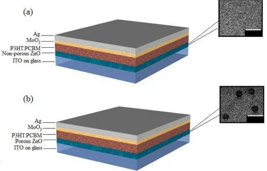
The effect of porous ZnO layer on the OPV device performance was systematically investigated by comparing such devices with the reference OPV device employing non-porous ZnO layer. The OPV device structures fabricated for these studies (ITO/ZnO/P3HT:PCBM/MoO3/Ag) are illustrated in Fig. 1. The reference structure has a
non-porous ZnO layer as shown in the scanning electron microscopy (SEM) image in Fig. 1(a) and the device with a highly porous ZnO layer is shown in Fig. 1(b). For these structures, indium doped tin-oxide on glass was used as the substrate. ZnO spin-coated from ZnO sol-gel
and MoO3 deposited using a thermal evaporator were used as the electron and hole selective
layers, respectively. A 1:1 ratio of P3HT:PCBM (40mg/mL) in cholorobenzene solvent was used as the active layer and silver, deposited using the thermal evaporator, was used as the electrode. For the reference structure [Fig. 1(a)], the ZnO layer was prepared by spin-coating from ZnO sol-gel using the method described elsewhere [12] with zinc acetate dihydrate as the precursor and anhydrous ethanol as the solvent. The as-coated ZnO layer was then annealed at 200°C to obtain the ZnO electron selective layer. For the porous structures, the porosity was further induced in the ZnO layer with the addition of poly ethylene glycol (PEG) to the aforementioned ZnO sol-gel solution. Here the role of the PEG is to form an organic template to support ZnO and assist in the formation of a porous structure by inducing a phase separation between the solvent and zinc oxide adsorbed on PEG [16]. Upon subsequent annealing at 200°C, the PEG was removed and the porous ZnO layer was obtained. The resultant thickness of the ZnO layer is ~40 nm regardless of the porous or non-porous structure. The rest of the processing was identical for both porous and non-porous structures. The P3HT:PCBM active layer was spin-coated, followed by annealing 100°C for 10 min. The samples were then transferred to the evaporator for the deposition of MoO3 hole selective
layer and silver electrode, which were then subjected to post-annealing in N2 ambient at
160°C for 10 min.
Fig. 1. Schematic representation of OPV devices with (a) a non-porous ZnO layer and (b) a highly porous ZnO layer, along with respective SEM images showing the porous and non-porous ZnO layer in the respective devices (scale bars: 20µm).
2.2 Characterization
Current density-voltage (J-V) measurements for the fabricated devices were performed under a solar simulator using AM1.5G filter calibrated to obtain simulated light intensity of 100 mW/cm2. From the J-V measurements, the vital device performance parameters, namely, the
open circuit voltage (Voc), short circuit current (Isc), fill factor (FF) and efficiency (η) were
extracted. Incident Photon to Charge Conversion Efficiency (IPCE) spectra were measured using photovoltaic cell spectral response and external quantum efficiency (EQE) measurement system. The system has a Xenon light source and triple grating monochromator. Absorption/reflection spectra and haze factor measurements were taken using PerkinElmer UV/Vis/NIR spectrophotometer system. The system includes a spectral span from 175 to
3300 nm and an integrating sphere for high precision reflectance and scattered transmittance measurements.
3. Results and discussions 3.1 Porous vs. non-porous devices
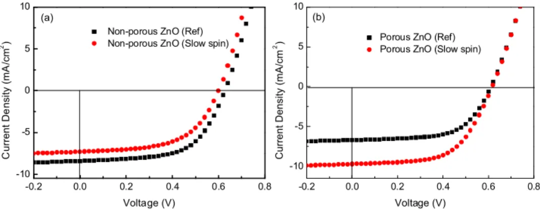
Initially, the optimal processing conditions for spin-coating the ZnO sol-gel and active layer for the reference OPV device was established. The OPV devices with the porous ZnO layer, using a ZnO:PEG ratio of 4:1, were then fabricated using the same parameters for spin-coating the active layer (2000 rpm). However, contrary to expectations, these porous devices showed degraded performance compared to the reference samples. While the open circuit voltage and the fill factor of the porous and non-porous devices were similar, the short circuit current density of the porous structure OPV was lower compared to the reference (Fig. 2).
An adequate filling of pores is an important criterion to obtain high efficiency in porous devices. In addition to the pore size, the spinning speed of the active layer material also has an impact on the filling of pores. Experiments were carried out to see the effect of the spinning speed of the active layer on the device performance. A slow speed (800-1000 rpm) can lead to a better filling of the pores. The slow speed also results in thicker active films, which in turn enable stronger absorption of light. However, the thickness of the active layer in OPVs are typically kept to below 200 nm, as thicker films cause higher series resistance and longer charge transport distances. This can result in lesser charge collection and hence poorer device performance [15]. J-V curves in Fig. 2(a) show that a slow spinning speed leads to poor performance of the reference devices with non-porous ZnO layer due to thicker active layer. However, in the case of porous ZnO devices, a slow spinning speed leads to a remarkable improvement in performance (Fig. 2(b)). In the case of the reference devices, the downside of using thicker layers comes into play. However, for the porous OPVs, the improved penetration which comes with the slower spinning speed, leads to improved surface area, interfacial contact and charge collection, which complements the increased optical absorption in the thicker active layer. Table 1 lists the extracted device parameters of these devices and it can be observed that the porous OPV shows enhanced performance even compared to the best performing reference sample. The slow spinning speed for the active layer coating was thus used for the device with porous ZnO film whereas fast spinning speed was used for the device with non-porous ZnO film in the rest of the experiments.
-0.2 0.0 0.2 0.4 0.6 0.8 -10 -5 0 5 10
Porous ZnO (Ref) Porous ZnO (Slow spin)
Curr ent Density (mA/ cm 2 ) Voltage (V) (b) -0.2 0.0 0.2 0.4 0.6 0.8 -10 -5 0 5 10
Non-porous ZnO (Ref) Non-porous ZnO (Slow spin)
C u rrent De nsit y (m A /cm 2 ) Voltage (V) (a)
Fig. 2. Current density-voltage (J-V) characteristics of OPVs with (a) porous ZnO layer and (b)non-porous ZnO layer, with the active layer coated at different spinning speeds (reference spin-coating speed: 2000 rpm; slow spin-coating speed: 800-1000 rpm).
Table 1. Device parameters of porous and non-porous ZnO OPV with the active layer spin-coated at different spinning speeds (reference spin-coating speed: 2000 rpm; slow
spin-coating speed: 800-1000 rpm)
Voc (V) Isc (mA/cm2) FF η
Porous ZnO OPV (reference) 0.610 −6.688 0.61 2.49%
Porous ZnO OPV (slow spin-coating)
0.617 −9.693 0.59 3.50%
Non-porous ZnO OPV
(reference) 0.627 −8.937 0.60 3.15%
Non-porous ZnO OPV
(slow-spin coating) 0.590 −9.275 0.38 2.07%
3.2 Influence of porosity on OPV devices
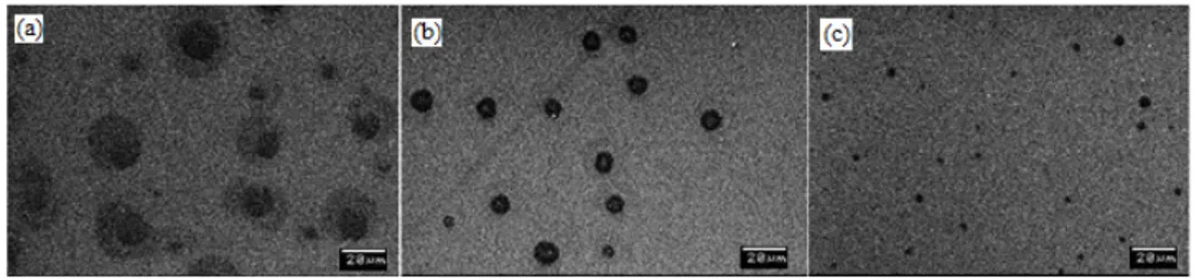
To study the effect of PEG concentration on the porosity and the device performance, ZnO sol-gel solutions with varying PEG concentrations were used to spin-coat their porous ZnO layer. In these experiments, ZnO-to-PEG ratios of 3:1, 4:1 and 5:1 were studied. The ZnO:PEG ratio above 5:1 was found to be too minute to result in sufficient porosity in the ZnO layer and ZnO:PEG ratio below 3:1 has overconcentration of PEG and hence proved unsuitable. Figure 3 shows the SEM images of the resulting porous ZnO layers with different ZnO:PEG ratios. From the images it can be seen that the concentration of PEG in the solution has marked influence on the porosity of the resultant layer.
Fig. 3. SEM images of porous ZnO layer with the ZnO:PEG ratio of (a) 3:1 (b) 4:1 and (c) 5:1.
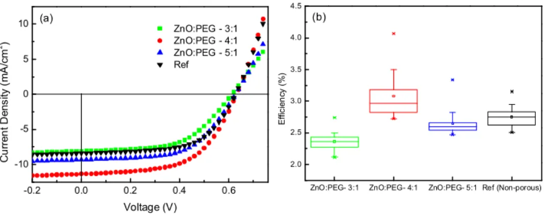
From the J-V curves (Fig. 4(a)) and Table 2, listing the extracted parameters of the fabricated OPV devices with the best performance for different PEG ratios used in porous ZnO layer and that of the reference device with non-porous ZnO layer, it is apparent that the ZnO:PEG concentration of 4:1 provides the best results. From Fig. 4(b), which compiles the efficiency extracted from 24 devices for each ZnO:PEG ratio, the trend of efficiency is evident. There is an increase in the efficiency when the ZnO:PEG ratio is decreased from 5:1 to 4:1, which can be attributed to the increased pore size and porosity due to the increase in PEG concentration (as can be seen from the SEM images). However, further decrease in the ZnO:PEG ratio to 3:1 leads to deteriorated performance. From SEM images it can be observed that, for the ZnO:PEG ratio of 3:1, though the pores appear larger, they are less well-defined and traces of excess PEG is visible, which affects the device performance adversely.
Incident photon-to-charge conversion efficiency (IPCE) spectra of the devices with different ZnO:PEG ratios are presented in Fig. 5. The IPCE data follows the trend of short circuit current density and thus supports the correlation between the porosity and the device performance as discussed.
-0.2 0.0 0.2 0.4 0.6 -10 -5 0 5 10 ZnO:PEG - 3:1 ZnO:PEG - 4:1 ZnO:PEG - 5:1 Ref C u rr en t D ens ity ( m A /cm 2) Voltage (V) (a)
ZnO:PEG- 3:1 ZnO:PEG- 4:1 ZnO:PEG- 5:1 Ref (Non-porous)
2.0 2.5 3.0 3.5 4.0 4.5 Effi ci en cy ( % ) (b)
Fig. 4. (a) Current density-voltage (J-V) characteristics of OPVs employing porous ZnO layer with different ZnO:PEG ratios and non-porous reference cell (b) efficiency trend for the cells with different PEG ratios and non-porous reference cell extracted from 24 devices. The horizontal lines in the box denote the 25th, 50th and 75th percentile values while the error bars denote the 5th and 95th percentile values.
Table 2. Device parameters of the best porous ZnO OPV with different ZnO:PEG ratios and their non-porous reference device fabricated
ZnO:PEG ratio Voc (V) Isc (mA/cm2) FF η
3:1 0.613 −8.095 0.55 2.74% 4:1 0.632 −11.338 0.57 4.07% 5:1 0.627 −9.310 0.57 3.34% Ref 0.627 −8.397 0.60 3.15% 400 500 600 700 0 20 40 60 80 IPCE ( % ) Wavelength (nm) ZnO:PEG -3:1 ZnO:PEG -4:1 ZnO:PEG -5:1) Ref (non-porous)
Fig. 5. IPCE spectra of OPVs employing ZnO layer with different ZnO:PEG ratios and non-porous reference cell.
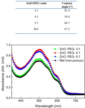
To understand the effect of PEG concentration on the ZnO layer characteristics, contact angle and absorption measurements were taken. Contact angle measurements provide information on the quality of the layer under study in terms of wettability and adhesion properties. Layers with good wettability and adhesion have smaller contact angles. Table 3
lists the results of the contact angle measurements for the porous ZnO layers with various ZnO:PEG ratios. From Table 3 it can be seen that the wettability is most favorable for the ZnO:PEG ratio of 4:1. For the ZnO:PEG ratio of 3:1, the wettability is substantially compromised and this may be due to the excess PEG present in the film. Absorption spectra of the active layers deposited on the porous ZnO layers with various ZnO:PEG ratios and on the non-porous ZnO layer are shown in Fig. 6. (Note: Herein, we added the absorption spectrum of the active layer deposited on the non-porous layer for the sake of comprehensiveness of the data. However, it is not a fair comparison between the absorption of active layer on the porous and non-porous films because the spin-coating speeds are not the same. The spin coating speed of 2000 rpm was used for non-porous ZnO whereas slow spin speed of 800-1000 rpm is used for porous ZnO to obtain the optimum device performance.) As can be seen from Fig. 6, the porous ZnO structure with the ZnO:PEG ratio of 4:1 exhibits higher optical absorption at all the wavelengths. The absorption profile of the sample with the ZnO:PEG ratio of 3:1 is markedly lower than the samples with other ratios of ZnO:PEG. The increase in the PEG concentrations in the porous ZnO layer with 3:1 ZnO:PEG left traces on the sample and adversely affected the spin-coating of the active layer and hence the absorption. From both measurements, the ZnO:PEG ratio of 4:1 was found to be the best for porous ZnO layer. The contact angle and absorption results of the samples were correlated to the device performance.
Table 3. Contact angle measurements of the ZnO layer in different ZnO:PEG ratios
ZnO:PEG ratio Contact
angle (°) 3:1 81.9 4:1 59.4 5:1 64.7 Ref. 67.2 400 500 600 700 0.0 0.2 0.4 0.6 0.8 1.0 Ab sorbance (Arb. U nit) Wavelength (nm) ZnO: PEG- 3:1 ZnO: PEG- 4:1 ZnO: PEG- 5:1 Ref (non-porous)
Fig. 6. Absorption spectra of the active layer deposited on porous ZnO layer with different ZnO:PEG ratios and on non-porous ZnO layer. A slow spin speed of 800-1000 rpm is used for porous ZnO whereas spin speed of 2000 rpm is used for non-porous ZnO.
3.3 Haze factor of porous ZnO layers
Employing the porous ZnO layer in OPV leads to notable improvement in the device performance and this may be mainly due to light trapping, increased absorption and enhanced surface area, interfacial contact and charge collection by sufficient pore-filling. The pores induced by PEG in the porous ZnO structure act as light scattering centers. This scattering increases the light path length, leading to improved absorption, which would further enhance the device performance. This can be verified using haze factor measurements. Haze factor studies are commonly used to quantify the scattering of transmitted light from a textured conductive oxide layer [24]. Haze factor can be described as the ratio between the total and diffused transmittance from the textured surface. To study the light scattering effects of the porous samples, transmission measurements were also carried out on the ZnO films coated ITO samples. Results of the total transmission studies on these samples are depicted in Fig. 7(a) and results of diffuse transmission studies in the inset of Fig. 7(a). Figure 7(b) shows the extracted haze factor results. Haze factor was the highest for the sample with ZnO:PEG ratio of 4:1 and agrees well with the rest of the results. The increased scattering in this sample, leads to improved light trapping and absorption and hence aids in enhancing the efficiency of porous OPV devices compared to the reference non-porous OPV devices.
300 400 500 600 700 800 0 20 40 60 80 100 T rans m itt anc e ( % ) Wavelength (nm) ZnO: PEG- 3:1 ZnO: PEG- 4:1 ZnO: PEG- 5:1 Ref (a) 300 400 500 600 700 800 0 10 20 30 40 50 Di ffus e T ran sm itt anc e (% ) Wavelength (nm) 400 500 600 700 800 0.1 0.2 0.3 0.4 0.5 0.6 0.7 H aze F a ct o r Wavelength (nm) ZnO: PEG- 3:1 ZnO: PEG- 4:1 ZnO: PEG- 5:1 Ref (b)
Fig. 7. (a) Total transmission (inset: diffused transmission) spectra and (b) the haze factor of the porous ZnO layer using different ZnO:PEG ratios and non-porous ZnO (reference).
3. Conclusions
With the introduction of high level of porosity in the ZnO electron selective layer in an inverted OPV, the ZnO layer acts as a scattering-center. The superior performance of the OPV device with highly porous ZnO layer is attributed to the porous layer created and controlled using polyethylene glycol template with an optimized ZnO:PEG ratio and active layer spin-coating speed. The highly porous ZnO layer provides increased light trapping, the role of which has been substantiated by device measurements and the layer characterizations performed. By employing the porous ZnO layer in the inverted OPV device, a current density of 11.34 mA/cm2 and an efficiency level of 4.07% have been obtained. This is a marked
improvement over the device performance of the reference sample with the non-porous ZnO layer. The use of such porous nanostructures can be extended to other metal oxides for both regular and inverted OPVs, which is being currently investigated. Porous metal oxide layers can also be applied to OPV systems with different active layer components, thus making porous light-scattering interlayers a highly portable method of efficiency improvement in organic photovoltaics.
Acknowledgments
This work was supported by the Singapore National Research Foundation under Grant No. NRF-CRP-6-2010-2 and NRF-RF-2009-09, the Singapore Agency for Science, Technology and Research (A*STAR) SERC under Grant Nos. 092 101 0057 and 112 120 2009, the New Initiative Fund and Joint Singapore-German Research Projects from Nanyang Technological University, and A*STAR SERC TSRP grant (Grant #102 170 0137).