Design Considerations
for
MMIC Distributed Amplifiers
San11 Ergun and Abdullah Atalar
Electrical and Electronics Engineering Department
Bilkent University,
06533
Bilkent
,
Ankara, TURKEY
phone:
+90-312-266-4307
e-mail: [email protected] .edu.tr
Abetract-The bandwidth of the input artificial line in a distributed amplifier is the main band limiting factor. By choosing this impedance prop- erly the bandwidth of a distributed amplifier can be maximized. A four section GaAs MES- FET distributed amplifier is designed using this strategy. The fabricated MMIC amplifier gives satisfactory performance. By adding proper length of series transmission lines in the drain
side, the gain and the gain flatness of the am- plifier can be further improved. This fact is presented via simulation results. The superior gain potential of cascode connected FETs is also demonstrated [2].
1. INTRODUCTION
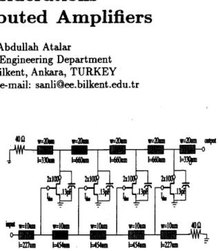
Distributed amplification is a way of adding device transconductances without adding device parasitic ca- pacitances. In this amplification technique the input and output capacitances of the FETs are linked through inductors to form artificial transmission lines. The two artificial lines, the gate-line and the drain-line. are de- signed to match the load and source impedances in such a way that the return losses are above some specified limit. This limit is typically taken to be 10 dB. By o p
timizing the gate-line impedance the frequency band of the amplifier can be maximized. The typical structure of a distributed amplifier is shown in Fig. 1.
2. AMPLIFIER DESIGN GUIDELINES
An artificial line is a cascaded constantlk network. The characteristic impedance of an artificial line is given
as,
Fig. 1: Schematic of a Distributed Amplifier When FETs are used a the active devices of dis- tributed amplifiers, the artificial lines become lossy (Fig. 2). The gateline contains a resistance in series with the capacitor, and the drain-line contains a con- ductance to the ground in parallel with the capacitor. The characteristic impedance expressions of these r e sistive artificial lines are more complicated.
Fig. 2: Simplified model of a MESFET For the gateline, the series resistance can be n e glected for frequencies at which the magnitude of the impedance of the capacitor is larger;
where, 2, = and w , = 2/m. For the drain-line, the shunt conductance can be n e
’0-7803-1772-6/94/%3.00
@
1994 IEEEglected for frequencies at which the magnitude of the conductance of the capacitor is larger;
Then, the characteristic impedance of the gate and drain-lines can be approximated with the Eq. 1, for w
<
wg and w>
W d , respectively [3].Ri,
C,,
C d r and R d , are shown in Fig. 2.The characteristic impedance of this artificial line is frequency dependent and drops to 0 at cut-off. But, still large bandwidths are obtainable. For a given FET, its input and output capacitances are known. Then, the problem is to find an optimum ( Z ~ , w c ) pair that m a - imizes the bandwidth of an artificial line. Note that, this optimum ( Z o , w , ) pair depends on the reference impedance level(e.g., 50R), and the bandwidth defini- tion (e.g, return loss greater than 10 dB). The gate capacitance of a MESFET is larger than the drain ca- pacitance, so the bandwidth of the gate-line is narrower than the bandwidth of the drain-line, and determines the overall bandwidth of the amplifier. Thus, the gate- line design must be done first. Then, the drain-line must be designed to match the load, and the phase shifts of the gate and drain lines must be equalized.
The gate and drain-lines must be terminated with resistive loads in order to have the unwanted signals dissipate on these resistive loads. Single resistors close to the artificial line impedances can do the termination job well.
The resistive losses are the causes of the attenua- tion in artificial lines. Hence, in gain determination the losses of the artificial lines can not be neglected. No matter how small the attenuation per section is, the total attenuation of a distributed amplifier increases ge- ometrically with increasing number of sections. On the other hand, the gain of a distributed amplifier increases arithmetically (addition of the transconductances). When the artificial line losses are included, the gain of a distributed amplifier can be found as the product of two terms (under perfect load and termination con- ditions):
A = Go x GI where
where Xd = w c / w d , x g = w g / w c , gm is the transconduc- tance of the FETs, c d is the total drain capacitance,
A, and A d are the attenuation per unit section of the
gate and drain-linea and
N
is the number of sections. Due to the geometric increaee of the attenuation, there exists an optimum number of sections,N ,
which maximizes the gain. The optimum number of sections is found aa [3]:By adding small capacitances to the drains of the FETs we can have a control over W d , the lower end of the bandwidth.
3. DESIGNS AND LAYOUTS
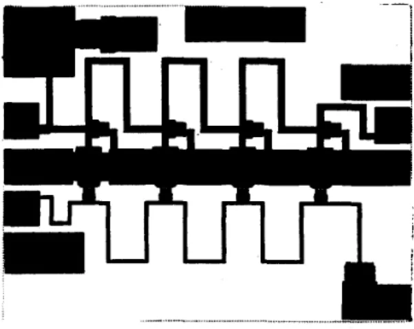
Following the guidelines given above, the first design shown in Fig. 1 is implemented. This amplifier uses
four identical sections although the optimum number of sections is found to be 6. Using a smaller number of sections than the optimum number gives a better gain flatness. About 5.5 dB gain is obtained in the 2-18 GHz
range. The layout of this amplifier is shown in Fig. 3. The simulation results are shown in Fig. 4 and Fig. 5.
... ~
L
Fig. 3: Layout of the First Amplifier This amplifier has been fabricated using GEC- Marconi’s F20 Foundry Process. This process utilizes 0.5 micron gate-length. The fabricated chip is mea- sured using an RF probe station and a network ana- lyzer. The measurement results are shown in Fig. 6 and Fig. 7.
To obtain larger gain we need FETs with larger trans- conductances. This can be obtained from larger FETs. But, larger FETs have larger gate capacitances which means narrower bandwidth. Nevertheless, there is way of increasing the gain without decreasing the band- width. The high frequency end of the bandwidth is determined by the gate-line, and dominantly by the
0
-T
I -
Fig. 4: Return Losses and Isolation of the First Am- plifier
Fig. 5: Gain of the First Amplifier
first section. Keeping the first FET small and using larger FETs in the other sections increases the effec- tive transconductance. Besides, the last section can be designed with a characteristic impedance to match the load and the previous sections with a higher character- istic impedance to increase gain [l].
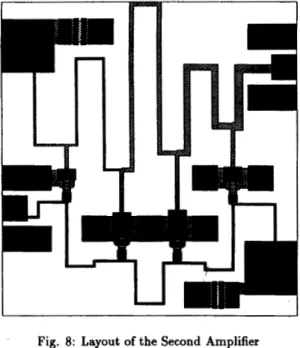
The gain flatness is very much related to the phase delay relations of the gate and drain-line sections. Adding short sections of transmission lines in series with the drains of the FETs gives us a control over
.-
,Fig. 6: Measured S21
-
I...)I
Fig. 7: Measured S11, S22 and S12
the phase delay of each section. By computer opti- mization the lengths of these transmission lines can be optimized t o give a very flat gain response. Using these considerations another amplifier is designed and fabri- cated. This amplifier has the same structure with the first one, as shown in Fig. 8, but has an improved gain response (-6.5 dB). The gain of this amplifier is plotted in Fig. 9.
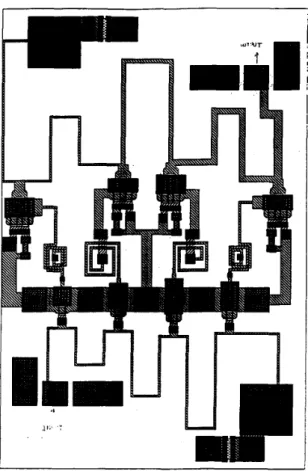
Fig. 8: Layout of the Second Amplifier In a distributed amplifier, the gain is closely related to the output impedance of the active device. Since the output impedance of the device is in parallel with the voltage controlled current source, the higher the output impedance is, the higher output voltage we ab- tain. Cascode connection (shown in Fig. 10) is a way of increasing the output impedance of the active de- vice [2]. Using cascode connected FETs the third am-
Fig. 9: Gain of the second design
Fig. 10: Cascode connected FETs
plifier shown n Fig. 11 have been designed and-fab- ricated. The bandwidth of this amplifier extends to 20 GHz and the gain is increased t o 10.5 dB (Fig. 12). Another advantage of cascode connection is the increase in the isolation of the amplifier (greater than 35 dB).
4. CONCLUSION
Three distributed amplifiers have been designed and fabricated. The first of these fabricated amplifiers have been received and measured. T h e results show that the fabricated chip operates as a distributed amplifier, and works well up to 20 GHz.
ACKNOWLEDGEMENT
This research has been supported by NATO-SFS un-
der the TU-MMIC project.
Fig. 11: Layout of the Third Amplifier
Fig. 12: Gain of the third design
REFERENCES
[l] W. Kennan, T.Andrade, Charles C. Huang, “A 2- 18 GHz Monolithic Distributed Amplifier Using Dual- Gate FETs,” IEEE Transactions on Electron Devices,
DEC. 1984
[Z] Eric M. Chase, W. Kennan, “A Power Distributed Amplifier Using Constant-R Networks,” IEEE Micro- wave and Milimeterwave Monolithic Circuits Sympo-
sium, June 1986
[3] James B. Beyer, S.N. Prasad, Robert C. Becker, James E. Nordman and Gert K. HohenWarter, “MES-
F E T Distributed Amplifier Design Guideline” IEEE Trans. on Microwave Theory and Tech., Vol. M T T - 82, March 1984 pp 268-275