DESIGN O F
ALL-POLE LOW-PASS LADDER FILTERS USING CURRENT-MODE
DAMPED INTEGRATORS
Omer Orulkunl Aydrn h e r Kargtlayan2 Mehmet Ali Tan3
l 2 Bilkent University,
Department of Electrical & Electronics Engineering. 06533 Bilkent, Ankara, TURKEY
e-mail: [email protected], karsilayQee.bilkent.edu.tr 3~ilicon Systems Inc.,
Tustin, CA 92680-7022, USA 14351 Myford Rd. MS C-100 e-mail: t t anm@ tus.ssi1 .com ABSTRACT
A
method for operational simulation of all-pole low-pass LC ladders filters by using current-mode damped integrators is introduced. The circuits obtained by this method need only current mirrors and capacitors and are convenient forrealization in CMOS technology as well as can be used in other technologies.
Figure
1. LC ladder p r o t o t y p e1. INTRODUCTION
LC two-ports have played an important role in the design of filters [I] because of their very low passband sensitiv- ities to element tolerances. Therefore, in recent years a considerable amount of effort have been devoted t o the de- sign of filters based on the operational simulation of LC ladqer prototypes 121. The basic building block in a fil- ter i an integrator with multiple input or multiple output, which ideally should have infinite DC gain. The distinguish- ing characteristic of the method introduced in this paper is that damped integrators are used instead of ideal integra- tors. T h e advantage of using damped integrators is that they are more realistic and easier to implement since any integrator is damped in reality due to finite DC gain. In addition, the integrator constructed from a current mirror as explained in this work has finite input conductance and capacitance, therefore can absorb the shunt parasitics, such that the most of the parasitics effectively create pole or zero shift instead of new parasitic poles or zeros.
In synthesis of the ladder filters, we use current-mode blocks, which provide a high linearity with wide dynamic range operating at high frequencies and low supply voltages. Furthermore, addition and multiplication by a scalar can be performed in a simpler manner using current-mode blocks. In the following section, the basic design procedure to generate the current-mode active circuit simulating the op- eration of an LC ladder prototype is introduced. Section 111
presents the simulation results for the current-mode ladder filter in comparison with the characteristics of the LC lad- der prototype.
$
-2. DESIGN PROCEDURE
Although the approach introduced here can be applied t o any LC ladder circuit, for the sake of simplicity, it is ex- plained by considering a third-order maximally flat low-pass minimum inductance LC ladder prototype. The ladder is terminated from both ends by 1-ohm resistors as shown in Fig. 1. By writing the node voltages in terms of mesh currents, and conversely the mesh currents in terms of the node voltages in s-domain, the signal flow-graph (SFG) cor- responding to the LC ladder prototype in Fig. 1 is easily ob-
0-7803-3073-0/96/$5 .OO 01996 IEEE
tained as shown in Fig 2. Note that the integrator blocks
I I
F i g u r e 2. Signal-Flow Graph of the LC ladder pro- t o t y p e
in the signal-flow graph are lossless integrators. However, the integrators considered in this work are damped. There- fore, we must device an approach t o convert this signal-flow graph to an equivalent one which is built by using damped integrators.
This approach basically propagates the source termina- tion resistor toward the other end of the ladder by leaving resistors in parallel with the capacitors and in series with the inductors as will be explained in the following.
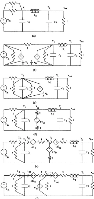
The first step is t o convert the 1-ohm source termination resistor into two 2-ohm resistors in parallel as in Fig. 3(a). Then we use the &-shift property [3] t o convert one of the 2-ohm resistors into the equivalent combination of vertical resistors and voltage controlled current sources (VCCS) as shown in Fig. 3(b), which are parallel t o the input voltage source ut,, and the capacitor
Ci.
Here, the resistor and the VCCS which are parallel to vi,, can be ignored since they only effect the current of vln without changing the internal node equations. Next, the 2-ohm resistor which is paral-lel to CI is replaced by two 4-ohm resistors in p a r d e l a.s
shown in Fig. 3(c). Then, the current source and the 4-ohm resistor parallel to it are converted t o a voltage controlled voltage source (VCVS) in series with two 2-ohm resistors as in Fig. 3(d). As the next step, we use the U,-shift prop- erty [3] to convert one of the last created 2-ohm resistors into equivalent combination of two current controlled volt- age sources (CCVS) and resistors connected series to them at both sides of the node designated by “w12”, as shown in
Fig. 3(e). Finally, we convert the voltage controlled volt- age source connected series with a 2-ohm resistor, which are vertically connected to node designated by “ ~ ~ 2 ” t o a
current source controlled by vin in parallel with a 2-ohm re- sistor as shown in Fig 3(f). This step completes the circuit transformation that we need. All the steps explained above are depicted in Fig. 3.
Figure 3. Transformation of the LC ladder proto- type.
Now we can draw the signal-flow graph of the transformed circuit as shown in Fig. 4 by writ,ing mesh and node equa- tions in terms of the Laplace transforms of the variables V i n ,
i o , V I , i02, VIZ, i2 and 2 ) s . One can easily verify that the signal-flow graphs shown in Fig. 2 and Fig. 4 both realize the same transfer function, that is
1
Figure 4. Signal-Flow Graph of the transformed circuit.
Although the process of transforming an LC ladder proto- type into a new LC ladder circuit that contains damped integrators is explained here on a third-order LC ladder fil-
ter prototype, it can be easily realized that the same process can be continued further, in order t o apply the same pro- cedure t o higher order, that is longer, all-pole low-pass LC ladder prototypes.
It is interesting t o note that the signal-flow graph in Fig. 4 is composed of the subgraphs that are special cases of the generic signal-flow graph shown in Fig. 5(a). For in-
Figure 5. Basic signal-flow subgraph and the basic linear circuit realization.
stance, the subgraph at the input of the SFG in Fig. 4 has a constant incoming branch and constant outgoing branches.
To
obtain such a signal flow graph, C is chosen zero and gmi = 1, and gmpi = gmp2 = 1. The subgraph shown in Fig. 5(a) can be implemented by the linear circuit shown in Fig. 5(b). Let us just ignore the parasitic componentsC , , gop and Son for the moment. For the most part, these parasitics are absorbed in the entire circuit by the intended shunt components. For instance gop and go,, are absorbed by the the input conductance gmr of the following stage which is the same type of subcircuit and
C,
becomes shunt and increases the value of the actual capacitance of the in- tegrator that may be following the subcircuit under consid- eration. The linear circuit shown in Fig. 5(b) can be imple- mented by the current-mode building blocks as the CMOS current-mode low-voltage damped integrator [4] shown in Fig. 6. Since the capacitors C in both rails of the fully bal- anced circuit shown in Fig. 6 are connected in series, they are replaced an equivalent capacitor C / 2 . The transistors whose gates are connected t o Vcp and Vcn are the ones used for tuning the integrators, or in other words for tuning the transconductances of the current mirrors. The transistor sizes are computed from the necessary transconductance values, that are g m t , gmp, and gmn. Note that the branchII Simulated CCI = 20.8pF CL^ = 41.6pF CCI = 82.2pF CCI = 6.5pF
CL^
= 13.0pF Cc3 = 26.0pF CCI = 2.08pF CL^ = 4.16pF Cc3 = 8.32pFFigure 6. F u l l y balanced CMOS tunable current- mode low-voltage damped integrator.
transmittances in the signal-flow graph shown in Fig. 4 are normalized values with respect t o lrad/s and
la.
The transconductance corresponding t o the unit branch trans- mittance should be computed by C / ( 2 r f o ) , whereC
is the integrator capacitance and fo is the denormalization fre- quency.3. SIMULATION
RESULTS
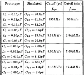
The signal-flow graph of the transformed circuit shown in Fig. 4 is constructed by using the circuit blocks described in Fig. 5 in order to examine the performance of the equivalent active network. The active implementation of the building blocks is realized using MOS transistors and capacitors by means of CADENCE and considering a 2-p double-metal double-poly CMOS technology. The active implementation basic building block integrator block is depicted in Fig. 6 . The simulation of the active network is performed for dif- ferent cutoff frequencies which means for different capacitor values. The performance of the active equivalent circuit is listed for different LC ladder prototypes in table 1. The magnitude characteristics of LC ladder prototypes and the corresponding active implementations are depicted together for comparison in Fig. 7 .
Cutoff (pr)
f
cpr 9 9 5 k H ~ 3 . 1 8 M H ~ 9 . 9 6 M H t -150z
-150 10 1os
1 ~.oo
1o6
Frequency (Hz) Frequency (Hz) -150 I -150 10 1o5
10 1o6
Freauencv (Hz) Freauencv /Hz) F i g u r e 7. Transfer characteristics of the p r o t o t y p eand a c t i v e f i l t e r s for various c u t o f f frequencies. The simulation results demonstrate that the performance of the active circuit is very close t o the performance of the prototype circuit for low frequencies, but there is a slight
Prototype C1 = O.16pF Lz = 0.32pH C3 = 0.16p.F Ci = 0.05pF L2 = 0.1OpH C3 = 0.05pF CI = 0 . 0 1 6 p j Lz = 0.032pL6 C3 = 0.016pI
4
= 0.005pI L2 = 0 . 0 1 p H C3=
0.005pI h t o f f (sim: fcfcsim 9 3 8 k H z 2 . 8 4 M H r 7 . 6 8 M H z 1 7 . 3 M H zTable 1. S i m u l a t i o n results for a c t i v e f i l t e r s filters w i t h v a r i o u s cutoff frequencies.
hump at higher frequencies. It is verified by simulation that the reason for this hump is the parasitic capacitances in the active circuit. The effect of the parasitic capaci- tances prevents an exact pole-zero cancelation and results in the hump. But the hump does not cause a significant problem, for example for the filter with cutoff frequency at nearly lMHz, the signal is suppressed nearly by 60dB where the hump occurs. For filters with higher cutoff frequen- cies, we have observed that the filter characteristic slightly shifts toward the lower frequencies. However, the tuning capability of the blocks used in the active implementation enables us to correct the deviations from the expected per- formance. In Fig. 8, it is shown how the performance of the circuit with cutoff frequency at approximately 32 MHz is corrected by tuning. Although it may not be important since it is a filter, the DC gain of the filter is less than what is expected. This occurs due t o the input conductance of the mirrors are decreased and the absorbed output conduc- tances become significant. This deviation can be corrected also simply by tuning the transconductance of the input or
the output stage. Here, one should also note that the sim-
...
-80.. --P'oto'Ype --Simulation
-100' J
1 o5 IO6 10' lo8 1 0' Frequencv IHz)
Figure 8 . C o r r e c t i o n of the cutoff frequency for the
f i l t e r w i t h cutoff frequency n e a r l y 32MHz
ulations are performed with transistors with gate width of 2 p . Even better results can be obtained by using CMOS technologies with smaller feature sizes.
4. CONCLUSIONS
This work presents an approach for realization of the inter- nal operation of an LC ladder filter by a current-mode active circuit using current mirrors and capacitors only.
It
is ver- ified by simulation, considering CMOS 2-p technology and by a full-custom design using CADENCE design tools, that the implementation of the proposed method yields good re- sults. The tunability of the building blocks makes it possible t o correct the performance of the filter for higher frequen- cies. Although the approach is presented by a third-order example, it can be easily applied t o higher order LC lad- der prototypes by induction. The presented approach is discussed for all-pole low-pass LC ladder prototype. How- ever, it can be extended easily t o arbitrary configurations in order t o include also the elliptic, band-pass and high-pass LC ladder prototypes. Since the approach is independent of how the current mirrors are implemented.It
can be ap- plied by employing other current-mirrors such as cascode and improved Wilson current mirrors and other technolo- gies such as Bipolar, BiCMOS or GaAs. The same approach can be easily applied by using also voltage mode circuits, switched-capacitor and transconductance-C circuits since the approach finds a signal-flow graph build by damped integrators.REFERENCES
[l] R. Schaumann, K.
R.
Laker, and M. S. Ghausi. Design of Analog Filters: Passive, ActiveRC
and Swuitched- capacitor. Prentice-Hall, Englewood Cliffs, New Jersey, 1990.[2] J. Ramires-Angulo, M. Robinson, and E. Sanchez- Sinencio “Current-mode continuous-time filters: Two design approaches,” IEEE Trans. on Circuits. Systs.
11:
Ana. and Dig. Sig. Proc, vol. 39, pp. 337-341, June 1992.[3] Leon. 0. Chua, Charles A. Desoer, and Ernest S. Kuh. Linear and Nonlinear Circuits. McGraw-Hill, New York, NY, 1987.
[4] A.