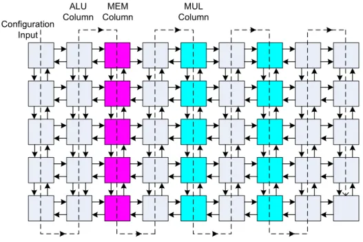
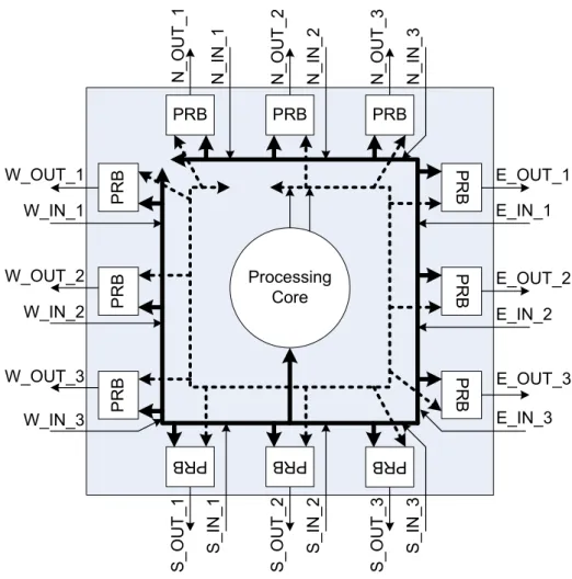
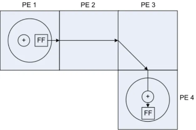
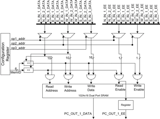
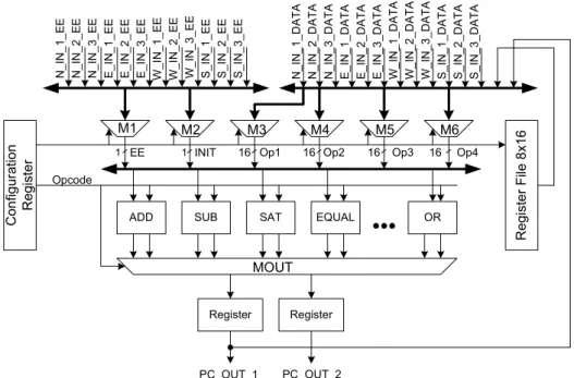
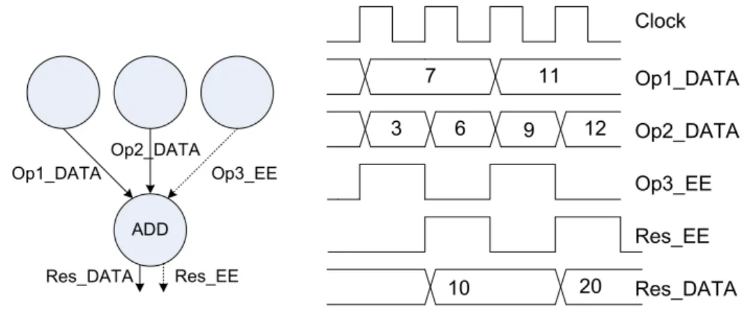
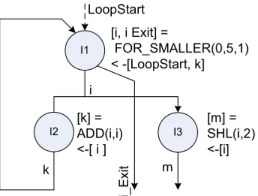
An execution triggered coarse grained recongigurable architecture
Tam metin
Şekil


Benzer Belgeler
The major contribution of the paper can be stated as follows: In a neural network based learning task of distributed data, it is possible to obtain an accuracy almost as good as the
As a result of long studies dealing with gases, a number of laws have been developed to explain their behavior.. Unaware of these laws or the equations
6) Liquids may evaporate in open containers. The particles with large kinetic energies can escape to the gas phase by defeating these intermolecular
made, the absorbance of at least one standard is measured again to determine errors that are caused by uncontrolled variables.. Thus, the deviation of the standard from the
As a result, public-key cryptosystems are commonly hybrid cryptosystems, in which a fast high-quality symmetric-key encryption algorithm is used for the message itself, while
It establishes the experimental foundations on which the verification of the theoretical analysis carried out in the classroom is built.. In this course the theoretical and
I would like to take this opportunity to thank the Near East University and especially the Faculty of Computer Engineering for giving me this chance to implement the knowledge
You are expected to write an essay on the theme of revenge in Poe’s short story “The Cask of Amontillado.” Feel free to discuss the topic from any angle that you wish, as long as
