LASER SYNTHESIZED GOLD
NANOPARTICLES FOR HIGH SENSITIVE
STRAIN GAUGES
A THESIS
SUBMITTED TO THE MATERIALS SCIENCE AND NANOTECHNOLOGY PROGRAM
AND THE GRADUATE SCHOOL OF ENGINEERING AND SCIENCE OF BILKENT UNIVERSITY
IN PARTIAL FULFILLMENT OF THE REQUIREMENTS FOR THE DEGREE OF
MASTER OF SCIENCE
By
Salamat Burzhuev
December, 2013
ii
I certify that I have read this thesis and that in my opinion it is fully adequate, in scope and in quality, as a thesis for the degree of Master of Science.
. Asst. Prof. Dr. Bülend Ortaç
I certify that I have read this thesis and that in my opinion it is fully adequate, in scope and in quality, as a thesis for the degree of Master of Science.
. Asst. Prof. Dr. Aykutlu Dana
I certify that I have read this thesis and that in my opinion it is fully adequate, in scope and in quality, as a thesis for the degree of Master of Science.
. Assoc. Prof. Dr. Hakan Altan
Approved for the Graduate School of Engineering and Science:
. Prof. Dr. Levent Onural Director of the Graduate School
iii
ABSTRACT
LASER SYNTHESIZED GOLD NANOPARTICLES FOR HIGH
SENSITIVE STRAIN GAUGES
Salamat Burzhuev
M.S. in Materials Science and Nanotechnology Supervisor: Assist.Prof. Dr. Bülend Ortaç
December, 2013
Recently, the conduction properties of nanoparticle films have received great deal of attention due to their unique properties attributed to quantum tunneling effect. Quantum tunneling effect, highly dependent on quantum barrier height and width, is very attractive for sensor applications. Resistive strain gauges based on gold nanoparticle (Au-NP) films show high strain sensitivity. These strain gauges are applicable for miniature applications because of its size. In addition, this nanoparticle films could be also used for various applications such as pressure and vapor sensors. Clean surfaces of laser generated Au-NPs provide high tunneling decay constant. Therefore, these films are promising for high sensitive sensor applications. In our study, the Au-NPs were directly synthesized in deionized water by nanosecond laser ablation method. The clean surface, size and aggregate clusters of Au-NPs offer advantages for high sensitivity strain sensor. We prepared Au-NPs films on flexible PDMS substrate by using hands-on drop-cast method. To obtain high gauge factor, we also investigated the nanoparticle concentration on the thin films. Laser-generated Au-NPs films demonstrated gauge factor of ∼300 for higher than 0.22% strain and ∼80 for the strain lower than 0.22%, which is favorably comparable to reported sensitivities for strain sensors based on Au-NPs. Mechanical characterizations for the prolonged working durations suggest long term stability of these strain sensors. We discuss several models describing conductance of Au-NP films in low and high strain regimes. To the best of our knowledge, the conduction of laser generated Au-NP films has not been studied up to date, and it is the first study that shows high strain sensitivity of these films. Au-NP films may be promising for sensor applications.
iv
Keywords: Laser ablation, gold nanoparticles, gold nanoparticle films, quantum tunneling effect, strain gauges, nanoparticle strain gauge
v
ÖZET
YÜKSEK HASSAS GERİLME ÖLÇERLER İÇİN LAZERLE
SENTEZLENMİŞ ALTIN NANOPARTİKÜLLERİ
Salamat Burzhuev
Malzeme Bilimi ve Nanoteknoloji, Yüksek Lisans Tez Yöneticisi: Yrd. Doç. Dr. Bülend Ortaç
Aralık, 2013
Son zamanlarda, nanoparçacık filmlerin elektriksel iletim özellikleri eşsiz kuantum tünelleme etkisi nedeniyle büyük ilgi görmektedir. Kuantum bariyer yüksekliğine ve genişliğine oldukça bağlı olan kuantum tünelleme etkisi, sensör uygulamaları için çok cazip. Altın nanoparçacık (Au - NP) filmlere dayalı dirençli gerilme ölçer, yüksek hassasiyetli davranış göstermiştir. Bu gerilme ölçer, boyutu nedeniyle minyatür uygulamalar için uygundur. Buna ek olarak, bu tür nanoparçacık filmler, aynı zamanda, basınç ve buhar sensörleri gibi çeşitli uygulamalar için de kullanılabilir. Lazerle oluşturulan Au-NP’ların temiz yüzeylere sahip olmasından dolayı yüksek tünel bozunma özelliğine sahiptir. Bundan dolayı yüksek duyarlı sensör uygulamaları için gelecek vaat etmektedir. Bizim çalışmamızda, Au- NP’lar doğrudan nanosaniye lazer ablasyon yöntemi ile su içinde sentezlenmiştir. Au-NP’lerin temiz yüzeyleri, boyutları ve kümeleri, yüksek hassasiyet gerginlik sensörü için avantajlar sunmaktadır. Pratik damlatma yöntemi kullanılarak Au- NP filmler PDMS esnek alt-tabaka üzerinde hazırlanmıştır. Yüksek ölçü faktörünü elde etmek için, filmler üzerindeki nanoparçacıkların konsantrasyonunu araştırdık. Lazer ile oluşturulan Au-NP filmlere %0.22’den fazla gerginlik uygulandığında g faktörünün ~ 300; daha düşük gerginlikler uygulandığında ise g faktörünün ~ 80 olduğu gösterdik. Au-NP’lara dayalı gerginlik ölçen sensörler, rapor edilen hassasiyetlerle karşılaştırılabilir. Uzun çalışma süreleri için mekanik karakterizasyonlar bu gerginlik ölçen sensörlerin uzun vadeli kararlılığını göstermektedir. Biz düşük ve yüksek gerilme rejimlerinde filmlerin iletkenliğini açıklayan çeşitli modeller sunduk. Bildiğimiz kadarıyla, lazerle üretilen Au–NP filmlerin elektriksel iletimi bu güne kadar çalışılmamıştır ve bu filmlerin yüksek
vi
gerginlik faktörüne sahip olduğunu gösteren ilk çalışmadır. Au-NP filmler sensörlerde umut verici uygulamalara yol açabilir.
Anahtar Kelimeler: Lazer ablasyon, altın nanoparçacıklar, altın nanoparçacık filmler, kuantum tünelleme etkisi, gerilme ölçer, nanoparçacık gerinim ölçer
vii
viii
Acknowledgement
I express my deepest gratitude to my supervisor Asst. Prof. Dr. Bülend Ortaç and Asst. Prof. Dr. Aykutlu Dâna. Without their guidance and supportive attitude, this thesis would not been possible.
I would like to thank Assoc. Prof. Dr. Hakan Altan for accepting to be one of my master’s thesis committee members and for judgments and helpful critics.
I also would like to thank the entire Ortaç group; especially, Canan Kurşungöz for carefully reading and helping for editing my thesis.
I’m thankful to UNAM members; especially, Ongun Özçelik, Ismail Kupa, Ruslan Garifullin, Serkan Karayalçın, Sencer Ayas and Hasan Güner for being helpful and for providing productive scientific environment during the course of my M.S. degree.
I am indebted to Dr. Selim Tanriseven my science teacher, for providing first sparks in science that led to birth of my interest in this field. I’m also thankful to Daniyar Marlisov for further increasing my interest in science through my undergraduate years.
I am thankful to my friends Kanat Jakshybekov, Nurbek Kakenov, Rinat Abdurahmanov and Eldiyar Djumataev for providing wonderful atmosphere.
I owe my profound gratitude to my family. Without their love and care it would not have been possible to do any of this.
ix
Contents
1. Introduction ... 1
1.1 Nanomaterials ... 1
1.2 Nanoparticle synthesis ... 5
1.3 Nanoparticle synthesis by laser ablation in liquids ... 5
1.4 Nanoparticle strain gauges... 6
1.5 Organization of thesis ... 7
2. Laser ablation method, nanoparticle synthesis and experimental results ... 8
2.1 Ultra short pulsed laser ablation ... 8
2.2 Nanosecond pulsed laser ablation ... 12
2.2.1 Thermal process of nanosecond laser ablation ... 13
2.2.2 Plasma generation and other processes ... 15
2.3 Formation of nanoparticles ... 16
2.3.1 Wavelength and fluence effect on nanoparticle formation... 20
2.4 Experimental results of laser synthesized Au-NPs in deionized water ... 23
2.4.1 Experimental setup of laser ablation in liquid ... 23
2.4.2 Characterizations of laser synthesized Au-NPs ... 24
3. Strain gauge ... 30
3.1 Conventional strain gauges ... 30
3.1.1 Liquid strain gauge ... 30
3.1.2 Metal foil strain gauges ... 32
x
3.1.4 Wheatstone bridge ... 35
3.1.5 Basic requirements of ideal strain gauge... 36
3.2 Nanoparticle strain gauge ... 37
3.2.1 Conduction properties of Au-NP films ... 37
3.2.2 Quantum tunneling effect... 39
3.2.3 Au-NP strain gauge ... 41
4. Laser synthesized Au-NP strain gauge ... 46
4.1 Strain sensor fabrication ... 46
4.1.1 SEM images of Au-NP film ... 48
4.1.2 Mechanical characterizations ... 50
xi
List of Figures
Figure 1-1 Absorption spectra of Au-NPs with different sizes and shapes.Adopted from Eustis et al. (2006) [8]. ... 4 Figure 2-1 150-fs laser pulses are used to ablate copper. Ablation depth per pulse
versus laser fluence is shown where and corresponding to fits. Adopted from Nolte et al. (1997) [31]. .... 11 Figure 2-2 SEM images of (a) nanosecond, (b) picosecond and (c) femtosecond laser
ablation of iron. Adopted from Leitz et al. (2011) [40]. ... 12 Figure 2-3 Ablation rate per pulse versus laser fluence graph of the graphite.
Theoretical estimation are shown by solid line and dashed line is treshould fluence. Ablation is performed by Q-switched Nd-YAG laser (1064 nm wavelength, 13 ns pulse duration) under vacuum conditions ( ). Adopted from Bulgakova et al. (2001) [44] ... 14 Figure 2-4 Shadowgraph images of cavitation bubble expansion during laser ablation of
silver in 18 mM PVP solution. Various phenomena are observed: a) optical emission, b) shockwave, c) cavitation bubble, d) secondary shockwave [51]. . 16
xii
Figure 2-5 Shadow graph pictures at various delay times of laser ablation of silver in water at laser fluences (a) and (b) . Adopted from Tsuji et
al. (2004) [59]. ... 18
Figure 2-6 Schematic representation of growth of nanoparticles when vaporized atoms (yellow balls), melted drops (red balls) and fragmented (red rectangle) particles exist in the solution. Note that dimensions are not to scale. ... 19 Figure 2-7 Platinum surface image after ablation with 1064 nm and 355 nanosecond
laser with fluences and . Adopted from Nichols et al. (2006) [25]. ... 21 Figure 2-8 Ablation yield versus laser fluence at different wavelength which is
measured by the optical density at 250 nm of platinum colloidal solution. Adopted from Nichols et al. (2006) [56]. ... 22 Figure 2-9 TEM images of laser synthesized platinum nanoparticles by 355 nm
wavelength with laser fluences a) , b) and c) . Selected area diffraction images are shown in insets. Adopted from Nichols et
al. (2006) [60]. ... 23
Figure 2-10 Schematic presentation of laser ablation in liquids and obtained Au-NP colloidal solution. ... 24 Figure 2-11 TEM image of Au-NPs. The inset shows the histogram of size distribution
calculated from TEM images. ... 26 Figure 2-12 XPS spectrum of Au-NPs. Two peaks correspond to 4f7/2 and 4f5/2 binding
energies. ... 28 Figure 2-13 Absorbance spectrum of Au-NP colloidal solution ... 29
xiii
Figure 3-1 Schematic representation of strain gauge working principle ... 31 Figure 3-2 Metal foil strain gauge under (a) no strain(no change in the resistance) (b)
tensile strain (zigzag pattern becomes longer and thinner resulting in increase of resistance) (c) compressive strain (zigzag pattern becomes shorter and thicker resulting in decrease of resistance). ... 34 Figure 3-3 Wheatstone bridge circuit ... 36 Figure 3-4 Shematic representation of electron hopping conductivity in Au-NP film.
Adopted from Zamborini et al. (2002) [69] ... 37 Figure 3-5 Exponential conductivity dependence on alkanethiol chain length. Adopted
from Wuelfing et al. (2000)[28] ... 38 Figure 3-6 Schematic demonstration of quantum tunneling effect between two metal
segments ... 39 Figure 3-7 Schematic representation of Au-NP strain gauge. Adopted from Herrmann
et al. (2007) [29] ... 42
Figure 3-8 Surface coverage effect on sensitivity of Pt nanoparticle strain gauge where a) fractional change in resistance vs. strain and b) corresponding gauge factor for different surface coverage. Adopted from Tanner et al. (2012) [75]. ... 45 Figure 4-1 Au-NPs coating on different surfaces: (a) on glass at different
concentrations; (b) on silicon nitride surface; (c) on PDMS at very high concentration. ... 47 Figure 4-2 Au-NPs film on PDMS substrate. (a) Au-NPs film after droplet was dried.
(b) After platinum contacts were deposited by PECS. ... 48 Figure 4-3 SEM image of Au-NPs thin film on PDMS substrate ... 49
xiv
Figure 4-4 Schematic demonstration of Au-NPs strain gauge. Pt contacts are at the edges of sensor and Au-NPs are shown as yellow balls. Note that, dimensions are not to scale. In the left side, Au-NP film is in the initial state where there is no strain and resistance of film is R. In the right side, strain is applied to Au-NP film that increases distances between nanoparticles and aggregated clusters resulting in resistance increase of R. ... 51 Figure 4-5 I-V curve of Au-NP film under different strains. ... 52 Figure 4-6 Resistance change of Au-NP film that have different initial resistances upon
applying strain. ... 53 Figure 4-7 Resistance change response of Au-NP films while applying strain. Fit 1 and
2 are the corresponding linear and exponential functions. Also, metal foil strain gauge response is shown for comparison which have gauge factor of 2 (dashed-dotted line). ... 55 Figure 4-8 Alternating strain response of Au-NPs strain sensor (at 1Hz frequency). ... 57 Figure 4-9 Simple circuit model of Au-NPs thin film and histogram of number of
samples vs. resistance of the samples. ... 59 Figure 5-1 Au-NP resistance change due to humidity change. “ON” is when dry air is
1
Chapter 1
Introduction
1.1 Nanomaterials
Nanomaterials are materials that show different properties than bulk material. Their properties strongly depend on their size. It’s very interesting, because same material’s properties can be tuned if precise control of size and shape is possible. These small materials can provide very unique properties that may lead to new discoveries and applications. Nanomaterials have very long history. For example; Lycurgus Cup is a 4th-century Roman glass cage cup having green color in the day light (reflected light), and red color if light is shined from inside (transmitted light). These striking properties of the Lycurgus cup appear due to Au-NPs that are in glass [1]. Immense progress in the field of nanomaterials is continuing nowadays. Nanomaterials can have unique quantum properties such as quantum confinement effect and ballistic electron transport. Quantum confinement effect can be observed in quantum dots, which are semiconductor nanoparticles, which have different optical and electrical properties than that of bulk. Ballistic electron conduction is observed in graphene in which electron mobility is very high due to characteristic of two-dimensional Dirac fermions where electrons move with relativistic speeds[2]. Also, nanomaterials show very exciting properties from the classical point of view. For example, one can obtain large surface
2
area from nanoparticles. Surface to volume ratio of spherical particle will be proportional to R-1 where R is the radius of particle; so, for nanoparticles that are just few nm (10-9 m) this ratio is very huge. This property of nanomaterials is useful for catalysis application because chemical reactions occur near the surface, large surface area can increase total yield of the reaction[3]. Also, if normally hydrophobic surface became nanostructured, super-hydrophobic surfaces can be obtained because high surface roughness provides high contact angle. Perhaps, best example is the lotus leaf which has a super-hydrophobic surface due to its high surface roughness[4]. On the other hand, hydrophilic surfaces present high hydrophobicity when surface roughness is increased[5]. Melting point of nanoparticles is also different from the bulk materials. It depends on the size of nanoparticles; such that the smaller the size, the lower the melting point[6].
Semiconductor nanomaterials such as quantum dots have unique properties. Their optical and electrical properties are highly dependent on their sizes[7]. When the particles become smaller than Bohr’s radius, particle’s properties become strongly dependent on its size [8]. This property comes from quantum confinement effect where both electrons and holes are confined in the quantum well, whose width is the diameter of nanoparticle. Generally, quantum dots are semiconductors and the band gap and size of them are inversely related to each other because of the quantum confinement effect[9]. With the current technology, it is possible to make highly controllable quantum structures[10]. Plenty of applications can be done by these quantum structures such as photodetectors [11], light-emitting diodes(LED) [12], lasers[13] and transistors [14].
3
Carbon based nanomaterials also show very promising properties. Most popular carbon based nanomaterials are carbon nanotubes and graphene that are composed of carbon atoms, only. Carbon nanotubes are one dimensional materials which have: very high mechanical strength[15]; and, if it is metallic, high electron mobility[16]; high thermal conductivity[17]. Generally, bundles of metallic and semiconductor carbon nanotubes mixture are observed. It is hard to separate these individual carbon nanotubes which is unfavorable for applications [17]. Graphene is one atom thick, two dimensional materials. These materials gained significant attention due to their unique electrical, mechanical and optical properties. Graphene is the strongest material; it has the highest electron mobility and it is nearly transparent [2, 18, 19].
Noble metal nanoparticles also have unique properties mainly because of their optical characteristics which depend on size, shape and dielectric constant of surrounding material. Metals have plenty of free electrons which can be oscillated when light is directed on the metal surface. Typically, this happens on the surface of metals which is in tens of nanometer order, depending on absorption coefficient. Mean free path of electrons in noble metals is , so electrons in the nanoparticles can oscillate without scattering if electric field is applied. Collective oscillation of electrons with respect to the ions in the metal called plasmons. Absorption cross section of these particles is much higher than that absorption of quantum dots. Surface plasmons are 2D electromagnetic fields which propagate in interface between metal and dielectric. Resonance condition occurs under certain coupling regime that provides information about refractive index change. One can obtain different colors ranging from red to blue by Au-NPs with diameters between 5-100nm. Also, a surface plasmon resonance
4
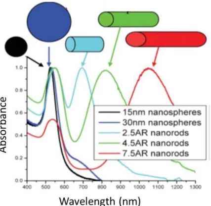
condition depends on the shape of particle. Particularly, gold (Au) nanorods absorption spectra can be tuned by changing aspect ratio of these nanorods (Figure 1-1). [8]
Figure 1-1 Absorption spectra of Au-NPs with different sizes and shapes.Adopted from Eustis et al. (2006) [8].
Noble nanoparticles can be used for sensing applications where mainly optical properties gains high interest. Applications of these nanoparticles such as Surface Plasmon Resonance (SPR) sensor and Surface Enhanced Raman Spectroscopy (SERS) are very promising. SPR sensors can be used to measure change in refractive index of a medium because SPR of Au-NPs depends on the dielectric medium. SERS is among the most popular topics because metallic nanoparticles can cause tremendous enhancing Raman signal of the absorbed molecule. This mainly happens because of large electric field enhancement near the surface of nanoparticles. [8]
5
1.2 Nanoparticle synthesis
Generally, nanoparticle synthesis methods can be classified as bottom-up and top-down methods. In the bottom up method, particles are built from fundamental building blocks such as atoms and molecules. This method generally requires less energy than top-down method. There are several methods which may be categorized as bottom-up method such as chemical vapor deposition (CVD), molecular self-assembly, sol-gel processes, electrodeposition, and so on[20]. Noble nanoparticles are generally synthesized by Turkevich method which was developed in 1951. In this method, Au and citrate is mixed in water where temperature, ratio of Au to citrate and amount of reagents govern nanoparticle size distribution[8].
In top-down method, the particle is made from bulk material by reducing its size. This technique generally requires more energy because of the binding energy of atoms in the bulk. Optical and e-beam lithography are very convenient fabrication methods that can be categorized as top-down methods[8]. In these methods, light and electrons are used to make patterns on the the surface. Due to diffraction limit, optical lithography cannot achieve small feature size. On the other hand, one can achieve small feature size by using e-beam lithography which is relatively an expensive technique. Other methods such as thermal evaporation, e-beam evaporation, laser ablation, arc-discharge method are also widely used[20].
1.3 Nanoparticle synthesis by laser ablation in liquids
Laser ablation is the material removal by focusing the laser light on the surface of target material. Laser light leads to heating of material causing material removal by vaporization, plasma generation, melting and fragmentation[21]. Commonly, pulsed
6
lasers are used for ablation in order to heat only irradiated area, not the whole surface, to prevent heat diffusion. Generally, shorter pulses lead to smaller heated area [22]. Laser ablation in liquid is another top down method for production of colloidal solution. In this method, nanoparticles are generated by focusing laser light on target material that is in the liquid medium. Interestingly, removed materials from the target can form nanoparticles. This method provides several advantages for nanoparticle synthesis. A main advantage of this method is that experimental setup is relatively simple, while it can provide synthesis of wide range of nanomaterials. Parameters of experimental setup can be classified as laser parameters and target parameters. Laser parameters are pulse duration, fluence (pulse energy divided by spot area), wavelength, repetition rate, number of pulses[21]. Target parameters are the type of the bulk target, type of the liquid and temperature of the system. Variety of nanomaterials can be obtained by laser ablation such as metals[23], metal oxides[24], noble metals[25], semiconductors[26].
Also, nanoparticles can be generated without surface ligands that may be valuable for several applications. Clean surfaces of these nanoparticles may be advantageous for several applications and if needed may be functionalized further.
1.4 Nanoparticle strain gauges
Strain gauges are used to convert mechanical deformations to electrical signals. Recently, conduction of Au-NP film was extensively studied. Conduction behavior of this film strongly depends on length of the linker molecules [27, 28]. After some time, researchers realized that Au-NP films can be used as sensitive strain gauges [29, 30]. High strain sensitivity of these sensors depends on tunneling decay constant that is
7
dependent on linker molecule[29]. Also, sensitivity can be increased by increasing size of nanoparticles or aggregates[29].
Laser generated nanoparticles have high tunneling decay constant simply because they do not have any linker molecules. In addition, nanoparticle size and aggregation of laser generated nanoparticle maybe advantageous for high strain sensitivity.
1.5 Organization of thesis
In the chapter 1, introduction to nanomaterials and its synthesis was discussed. Also, a very brief explanation provided about the laser ablation method and nanoparticle strain gauges. In chapter 2, we have discussed about laser ablation method. Laser heating; material ejection from target; and nanoparticle growth were briefly discussed. In the third chapter of this thesis, we described the synthesis of Au-NP by laser ablation method. Then, these nanoparticles were characterized by transmission electron microscope (TEM), absorption spectroscopy and X-ray photoelectron spectroscopy (XPS) for determining size and surface chemistry of these nanoparticles. In chapter 3, strain gauge working principles and basic requirements of these sensors are discussed. Basic explanation of Au-NP strain gauge together with brief literature overview is also given. In chapter 4, the description of laser generated Au-NP film fabrication by simple drop-cast method is given. Mechanical characterizations of these films reveal high strain sensitivity and moderate repeatability. We also develop numerical models to better understand the conduction behavior of Au-NP films. In the chapter 5, a brief summary of thesis and outlook is provided.
8
Chapter 2
Laser ablation method, nanoparticle
synthesis and experimental results
2.1 Ultra short pulsed laser ablation
Laser ablation is material removal by irradiating the laser light on the material. When the laser is shined on the surface of materials, due to electromagnetic nature of light electron clouds starts to oscillate, and electrons gain kinetic energy, then energy is transferred to lattice [31]. Particularly, in metals, light is absorbed mainly by free electrons. High amount of evaporation of metal occurs when lattice energy exceeds evaporation specific heat leading to ejection of material from the surface[22].
Evaporation of metals due to laser was intensively studied[32, 33]. Special attention gained by nanosecond, picosecond and femtosecond laser was gained due to presence of different evaporation regimes [31, 34]. Laser ablation was explained by two temperature model[35, 36]. In this model, temperatures of electron and lattice taken separately as and . Two temperature one dimensional model is given by following equations 2.1, 2.2, 2.3, 2.4:
9 2.2 2.3 2.4
where and are heat capacities (per unit volume) of electron and lattice; z-direction of laser light to the metal; P- is laser heating term (W/cm3); - electron-lattice coupling constant; - electron thermal conductivity; - heat flux; and are laser intensity, surface absorptivity and absorption coefficient of material, respectively[31]. Heat capacity of lattice is much higher than heat capacity of electrons which allows electrons heated for very high temperatures. If electron temperature remains smaller than Fermi energy ) ,where and are Boltzmann constant and Fermi energy, heat capacity of electron is proportional to temperature ( where C is constant)and non-equilibrium electron thermal conductivity is where ( ) is equilibrium thermal conductivity of metal. These equations have three different regimes which depend on , and which are electron cooling time, lattice heating time and laser pulse duration.[37]
For femtosecond pulses , electron-lattice coupling coefficient can be neglected as . Electron heat conduction term may be neglected in order to simplify equations. . [37]
10
After solving these equations, ablation depth can be found. Evaporation can be explained by equation 2.5:
2.5
where and are density and the specific heat of evaporation of metal; is the velocity of the evaporation front and is a constant depending on the material. Ablation depth per pulse is (
)where is absorbed laser fluency;
( and are density and the specific heat of evaporation of metal (per unit mass)) threshold laser fluency needed to evaporation with femtosecond laser pulses. This type of regime maybe advantageous for micro structuring as heat does not have enough time to diffuse so that smaller area can be evaporated[37].
11
Figure 2-1 150-fs laser pulses are used to ablate copper. Ablation depth per pulse versus laser fluence is shown where and corresponding to fits. Adopted from Nolte et al. (1997) [31].
Femtosecond laser ablation depth per pulse versus depth is shown in the Figure 2-1. Experimental results are fairly same with the theoretically predicted results. However, in the Figure 2-1 , two fits for femtosecond laser ablation results are shown. The first one corresponds to the fit which was explained above where optical penetration of material is which is nearly in agreement with well-known optical penetration depth. In the second fit, optical penetration depth is assumed to be changed because of high fluence. [31]
For the picosecond pulses following conditions are satisfied . Under certain assumption ablation depth can be found same as for the femtosecond pulses. However, in this regime electron heat conduction term was neglected which is not very appropriate assumption as electron heat conduction is in orders of picoseconds[38] .
For nanosecond pulses, , so we can assume that electron and lattice temperatures are same which simplifies equations 2.6.
2.6
Heat penetration depth can be shown by √ , where is heat diffusion coefficient ( ). This regime is studied by several groups[33, 39]. In this regime, light energy first melts metal and then evaporates it. The energy absorbed by metal per unit mass is
12
specific heat of evaporation. Condition for strong evaporation is √ [34]. For the nanosecond regime heat is propagated along the metal which leads to evaporation of larger layer than in previously explained regime.
Figure 2-2 SEM images of (a) nanosecond, (b) picosecond and (c) femtosecond laser ablation of iron. Adopted from Leitz et al. (2011) [40].
While picosecond and femtosecond lasers provide higher precision[31, 34, 40] as can be seen from the
Figure 2-2, nanosecond laser provides higher ablation yield[40] because nanosecond laser systems have higher power than picosecond and femtosecond laser pulses.
2.2 Nanosecond pulsed laser ablation
In the section 2.1, nanosecond pulsed laser heating process was described, while ablation mechanism was just touched. Material removal process and nanoparticle generation is further studied in this section.
13
2.2.1 Thermal process of nanosecond laser ablation
Miotello et al. (1999) explained ablation of material by normal vaporization, normal boiling, and phase explosion [41]. Vaporization occurs when a material changes its state from condensed state to vapor state. There is no threshold in vaporization which occurs on the surface. Vaporization which includes evaporation and sublimation near the boiling point can be explained by Hertz-Knudsen equation 2.7:
√ 2.7
where , and are condensation coefficient , equilibrium vapor pressure, ambient pressure and Boltzmann constant. Evaporation and sublimation occurs only in the surface of the condensed matter. On the other hand, normal boiling and explosive boiling present inside material. According to Miotello et al. (1999), normal vaporization doesn’t occur under short pulse ( ) ablation while pulse is sufficient[41].
Boiling is a fast vaporization and occurs when vapor pressure exceeds surrounding pressure. Normal boiling is similar to water boiling process that we face in our daily life. In normal boiling bubbles appear and temperature of water doesn’t change upon heating process. Both normal vaporization and normal boiling follows bimodal decomposition in which gas and liquid exists in equilibrium. Nucleation of the bubbles is heterogeneous during this process[41].
Phase explosion appears when material is suddenly superheated above boiling point near to critical thermodynamic point. In this regime spinodal decomposition and homogeneous nucleation of bubbles occurs[41]. Phase explosion is also commonly called “explosive boiling” of metals studied by Martynyuk et al. (1974) [42]. First,
14
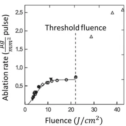
explanation of phase explosion of metals by intense laser light was proposed by Martynyuk [43]. By studying metal vaporization on microsecond time scales by laser pulses and electrical explosion of wires, they estimated critical temperature. In this study, he concluded that phase explosion will not present in the light pulses. However, recent studies demonstrate that phase explosion is main mechanism of material removal for [41, 44]. While, normal boiling is not a significant ablation mechanism in pulsed lasers since bubble diffusion process is very slow[41]. Bulgakova et al. (2001) have shown that there are threshold fluences for explosive boiling processes (Figure 2-3).
Figure 2-3 Ablation rate per pulse versus laser fluence graph of the graphite. Theoretical estimation are shown by solid line and dashed line is treshould fluence. Ablation is performed by Q-switched Nd-YAG laser (1064 nm wavelength, 13 ns pulse duration) under vacuum conditions ( ). Adopted from Bulgakova et al. (2001) [44]
15 2.2.2 Plasma generation and other processes
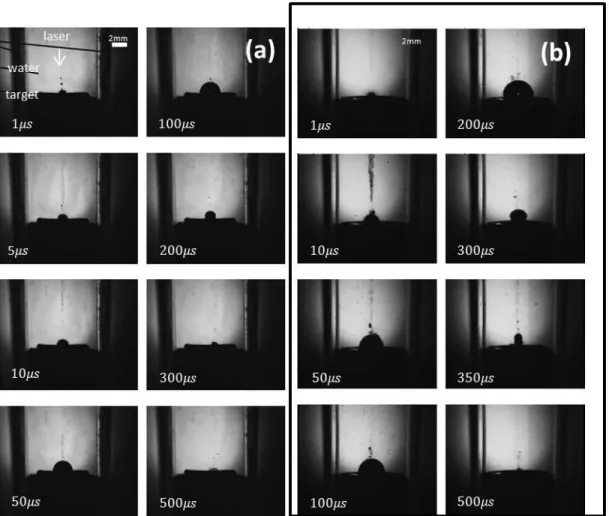
In order to understand whole picture of ablation, it is important to understand other process which take place during ablation such as photoionization, photomechanical stress and especially plasma generation. In the femtosecond laser ablation of polytetrafluoroethylene near the threshold fluence, emission of high-energy ions was observed. This can be described by columbic explosion due to photoionization process [45]. Asashi et al. studied laser ablation of organic microcrystals (quinacridone) where they observed photothermal ablation for nanosecond laser, and photomechanical process for femtosecond laser[46]. Because of photoionization and heating of the target, plasma plume can be generated. Plasma plume is a forth state of matter. Plasma is ionized gas composed of a lot of positively and negatively charges so that it can influence gas electrical behavior which is distinct from gas behavior. For nanosecond pulsed lasers, plasma plume life time is about twice of the pulse duration[47]. So, for nanosecond lasers light can be reabsorbed by plasma resulting in larger ablated area. On the other hand, with the picosecond and femtosecond regime, this will not happen. Plasma plume generated by laser ablation temperature and pressure are in the orders of several 103 K and several GPa [44, 48, 49]. Below the plasma regime ablation yield in liquid environment is slower than in vacuum because liquid confines solid[50]. However, when ablation regime above plasma threshold, ablation yield is higher in the liquid than in the vacuum because there is more confinement of plasma in the liquid [51]. Plasma releases its energy to liquid which generates cavitation bubble. Cavitation bubble expands and travels with the speed several times higher than sonic speed, having maximum radius in the order of
16
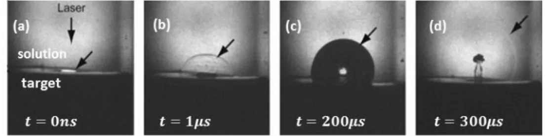
millimeters [51, 52]. Expansion of cavitation bubble leads to decrease in temperature and pressure become smaller than surrounding pressure. These processes lead to the collapse of bubble by emission of a shock wave.
Figure 2-4 Shadowgraph images of cavitation bubble expansion during laser ablation of silver in 18 mM PVP solution. Various phenomena are observed: a) optical emission, b) shockwave, c) cavitation bubble, d) secondary shockwave [51].
2.3 Formation of nanoparticles
Due to complexity of laser ablation process, several nanoparticle formation mechanisms will occur. During ablation process, the material is removed by vaporization, melting, fragmentation [53, 54]. For low nanosecond laser fluencies, normal vaporization is the main mechanism of material removal in laser ablation. Vaporized particles will nucleate and then coalescence and growth of nanoparticles will be observed [55]. Bulgakova et al. explained that main ablation mechanism during nanosecond laser ablation is due to explosive boiling under high fluences. For subthreshold fluences of laser, material ejection will be due to vaporization where vaporized atoms and melted droplets may appear[44]. For even higher fluencies amount of melted droplets can be increased further as well as fragmented particles appear, too. Researchers observed that size distribution of laser generated nanoparticles can be fitted to log normal function and some studies show that two modes can be
17
observed both for nanosecond and femtosecond pulsed laser ablation [56, 57]. Two modes may appear due to two different ablation mechanisms involved where normal vaporization is responsible for smaller particles while explosive boiling is the larger ones. In both of the studies, distribution of second mode – larger particles - is increased by increasing laser fluence [56, 57]. If the melted and fragmented particles are already detached from the surface, then nucleation may not be important because those particles already form nuclei, which are directly obtained during laser ablation process [21].
Most of the ablated nanoparticles are polycrystalline which means that nuclei coalescence should occur [55]. Generally, particles obtained by laser ablation have spherical shape meaning that nuclei coalescence may occur when lattice rearrangement occurs for decreasing interface energy. Also, there are several evidences that nanoparticle size is decreased when stabilizing agents such as polyvinylpyrrolidone (PVP) and sodium dodecyl sulfate (SDS), are used [51, 58]. So, growth of nanoparticle after ablation occurs.
18
Tsuji et al. (2003) investigated nanosecond pulsed laser ablation mechanism by microsecond-resolved shadowgraphy for Ag, Au, and Si targets. He observed cavitation bubble and straight jet generation where cavitation bubble is generated due to plasma (Figure 2-5). Straight jet’s ejection velocity and appearance were very distinct from cavitation bubble. Therefore, they conclude that straight jet generation may be due to ejection of clusters and droplets from the target[59].
Figure 2-5 Shadow graph pictures at various delay times of laser ablation of silver in water at laser fluences (a) and (b) . Adopted from Tsuji et al. (2004) [59].
19
One can consider combination of thermal effects and plasma effect on nanoparticle growth under high fluences. Nanoparticle generation will mainly depend on laser fluence. After certain threshold fluence explosive boiling will occur. These nanoparticles will mostly be formed by means of melted and fragmented particles; while, under lower fluences nanoparticle growth will be mainly due to vaporized atoms. However, combination of vaporized, melted and fragmented particle influence on nanoparticle formation can also be considered. In this case, vaporized, melted and fragmented particles all contribute to the growth of nanoparticle. In Figure 2-6, vaporized atoms can nucleate, coalesce, and grow for the nanoparticle formation. In addition, vaporized atoms can attach to surface of melted or fragmented particles resulting in the increase of particles’ size. Moreover, coalescence of melted particle may occur when their temperature is high enough. Fragmented materials may change its shape due to high temperature which will reduce its surface energy.
Figure 2-6 Schematic representation of growth of nanoparticles when vaporized atoms (yellow balls), melted drops (red balls) and fragmented (red rectangle) particles exist in the solution. Note that dimensions are not to scale.
20
2.3.1 Wavelength and fluence effect on nanoparticle formation
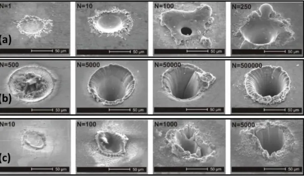
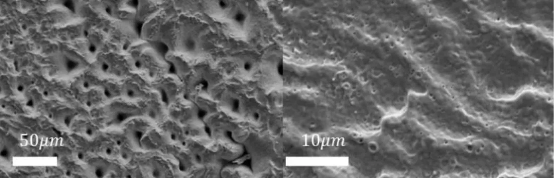
Researchers have shown that laser fluence play important role on size distribution and structure of particles [57, 60]. Nichols et al. have well explained the experimental results of nanosecond pulsed laser ablation of platinum (Pt) in water where the specific parameters, such as laser wavelength and fluence effects on nanoparticle size, structure and chemical composition, were studied [25, 56, 60]. They have used Nd:YAG laser operating at wavelength and nm with the pulse duration and , respectively. In this study, they have observed that surface of ablated Pt target have distinct properties for different operation wavelength. When targets are ablated by and laser light, shallow ripples and large craters ( diameter) are observed on the surface, respectively (Figure 2-7). On the other hand, when these targets are ablated by laser light, both shallow ripples and large craters appear on the same surface [25]. Because 355 nm light is strongly absorbed by generated nanoparticles, the fluence delivered to the target through colloidal solution is dramatically decreased while 1064 nm laser light is delivered much more to the target. For high enough fluences of nanosecond lasers explosive boiling may be responsible for material removal [41] which maybe the reason for observing such differences.
21
Figure 2-7 Platinum surface image after ablation with 1064 nm and 355 nanosecond laser with fluences and . Adopted from Nichols et al. (2006) [25].
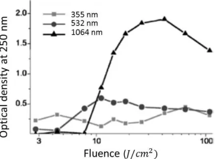
Mass yield of ablated material is largest for laser for fluences [56]. Tsuji et al. synthesized silver nanoparticles by laser ablation and studied wavelength dependence of mass yield and mean sizes [61-63]. He has also found that more nanoparticles can be obtained by 1064 nm laser light than the ones with 355 nm laser light which is focused on silver target when the light fluence is . On the other hand, when optical fluence of laser is , more nanoparticles were produced by 355nm laser than 1064 nm laser [62]. These results are fairly consistent with the results of Nichols et al. as shown in the Figure 2-8. Nichols et al. (2006) explained that under low laser fluences ablation yield is determined by absorption coefficient; however, this cannot explain Tsuji et al. results (absorption coefficient of silver is higher for 1064nm than 355 nm light [64]). Indeed, this discrepancy can be explained by combination of reflectivity and absorption coefficient on the ablation yield. Reflectivity of Pt for 1064 nm light is higher than 355nm light; therefore, ablation yield for low laser fluences is higher for 355 nm light than 1064 nm. For higher laser optical fluences (> ) more nanoparticles are
22
generated by longer wavelength because generated nanoparticles strongly absorb shorter wavelength resulting in decrease of delivered laser fluence to the target. For high enough fluences of nanosecond lasers explosive boiling is responsible for material removal [41] which maybe the reason for observing such differences.
Figure 2-8 Ablation yield versus laser fluence at different wavelength which is measured by the optical density at 250 nm of platinum colloidal solution. Adopted from Nichols et al. (2006) [56].
Particle sizes and size distributions also depend on operation wavelength because absorption of generated depends on wavelength. Two distinct modes of size distribution are observed which are fitted as a log-normal distribution. First mode is suggested to be due to thermal vaporization; and second mode is due to explosive vaporization. Laser ablation of Pt with 1064, 532, 355 nm nanosecond lasers under light fluences reveal spherically shaped and nonagglomerated nanoparticles with the size range [56]. On the other hand, when the fluence
23
of 335 nm laser is less than amorphous, gel-like, globular particles are found in the size range of [60]. At fluencies higher than for the same laser, gel-like materials are also observed and Pt nanoparticle number decreases while larger particles appear more frequently[60].
Figure 2-9 TEM images of laser synthesized platinum nanoparticles by 355 nm wavelength with laser fluences a) , b) and c) . Selected area diffraction images are shown in insets. Adopted from Nichols et al. (2006) [60].
2.4 Experimental results of laser synthesized Au-NPs in
deionized water
2.4.1 Experimental setup of laser ablation in liquid
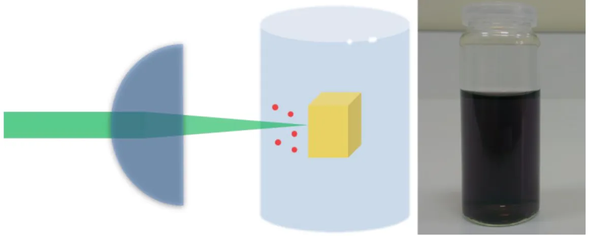
Au-NPs were obtained by laser ablation in deionized water. Au block (99.999%, Kurt J. Lesker) was cleaned by sonification in acetone prior to laser ablation without any additional purification. The generation of colloidal nanoparticles from Au block was carried out using a commercial pulsed Nd:YLF laser (wavelength: λ= 527 nm, 16 W average power, pulse duration t= 100 ns, pulse energy E= 16 mJ for 1 kHz). The cleaned Au block was placed in a glass vessel containing 23.5 mL of pure deionized water. The laser beam was focused on the target by using a plano-convex lens with focal length of 50 mm. The height of liquid layer over the Au target is ∼5
24
mm. The laser ablation was carried out for ∼10 min, and the laser beam is scanned over the target surface. During the laser ablation, the formation of colloidal nanoparticle solution with dispersed Au-NPs in liquid media was observed as a color change of the deionized water. After the laser irradiation, the color of the Au-NPs solution became dark-red. Basic experimental setup is shown where laser light is focused on the target material which is in the liquid in the Figure 2-10.
Figure 2-10 Schematic presentation of laser ablation in liquids and obtained Au-NP colloidal solution.
2.4.2 Characterizations of laser synthesized Au-NPs
Transmission electron microscope (TEM) is an imaging technique that uses electrons to image specimen. Electron source of TEM is typically tungsten which is connected to high voltage source up to 100-200 keV; so, electrons are emitted by means of field emission and thermionic emission. In order to focus electrons, magnetic lenses are used. Abbe diffraction limit is defined as
where λ is wavelength of light, nsinθ is numerical aperture (n-refractive index, θ- half angle of maximum light angle that can enter lens). So, in the air, maximum resolution of optical microscope is approximately half of the wavelength (about 550nm) which is ~ 225 nm. On the other
25
hand, electrons have very small wavelength compared to visible light wavelength. Wavelength of electron can be calculated by using de Broglie relation which is √ where m is mass of electron, e is electron charge, V is applied voltage, and h is Planck’s constant. So, if applied bias is in 100 keV, electron wavelength is ~ 0.5 10-11 m. For θ =10-2 radians, resolution can be calculated by above given diffraction limit formula which is . However, practical resolution limit of TEM is generally due to aberrations and distortions. TEM is the ultimate technique for nanoparticle imaging. Because electrons have very short wavelength, it is possible to see even crystal structure of nanoparticles. The structure of Au-NPs generated by nanosecond pulsed laser ablation were studied by TEM (TEM model FEI – Tecnai G2F30) system.
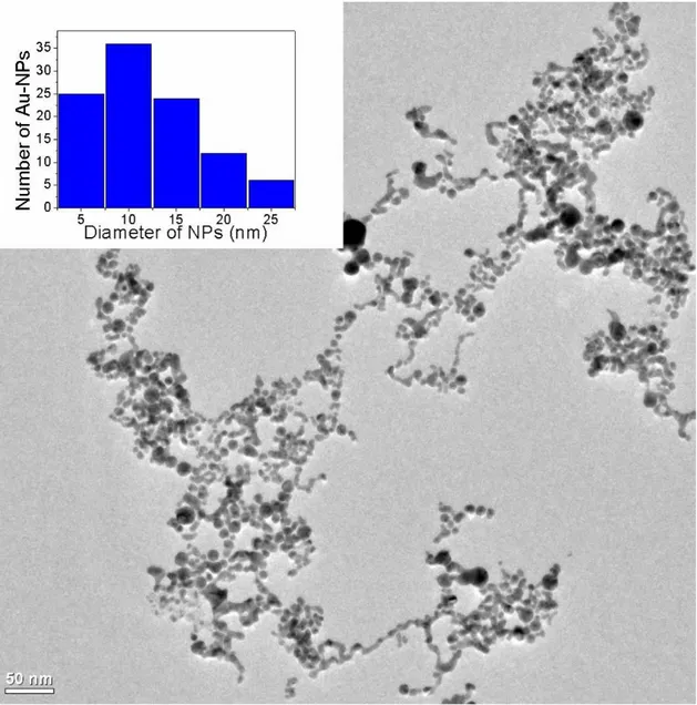
TEM sample was prepared by drop-casting solutions onto carbon-coated TEM grid. Representative TEM image of the Au-NPs is shown in Figure 2-11 (a), showing well dispersed spherical NPs. Size distribution of Au-NPs is given in Figure 2-11 inset. An average nanoparticles size of 13 nm is seen, with a distribution covering the range from 2 nm to 25 nm. Although, TEM is direct evidence of nanoparticle existence, this technique lacks for statistical analysis. TEM images are taken from very small area due to high magnification. Therefore, absorption spectroscopy should be applied in order to compare results.
26
Figure 2-11 TEM image of Au-NPs. The inset shows the histogram of size distribution calculated from TEM images.
XPS is widely used for surface analysis which measures elemental composition; chemical state of element; relative composition of constituents; and valence band structure. When target is irradiated by X-Ray, electrons are ejected from the surface by
27
means of photoelectric effect. By measuring amount and kinetic energy of electron, binding energy of electrons can be calculated. As binding energy of electron is unique for every element, it is possible to determine chemical composition of target surface. The surfaces of nanoparticles play a key role on the quantum tunneling effect. The elemental composition and the chemical state of the Au-NPs were studied by XPS. The XPS data were recorded with Au-NPs samples placed on silicon substrates. XPS measurements were performed on a monochromatic K-Alpha instrument (Thermo) operating at 12 kV and 2.5 mA. XPS spectra were collected with a photoelectron take off angle of 90° from a 200 µm diameter circular spot on the sample surface plane, energy steps of 0.1 eV, and pass energy of 30 eV. The control of the flow of the electrons to the surface is achieved by means of a well-controlled flood gun technique. XPS spectrum in the Figure 2-12, present two peaks located at 84.0 eV and 87.7 eV corresponding 4f7/2 and 4f5/2 [65, 66]. XPS spectrum reveals that the surface of Au-NPs is in low oxidation state. Thus, tunneling decay constant is higher than those particles which have surface ligands. Higher tunneling decay constant is significant for obtaining more sensitive strain gauges [29].
28
Figure 2-12 XPS spectrum of Au-NPs. Two peaks correspond to 4f7/2 and 4f5/2 binding energies.
UV-Vis spectroscopy is used measure absorbance of colloidal solution. This technique measures absorbance or reflection of solid and liquid samples from near-ultraviolet to near-infrared region. UV-Vis spectroscopy measures absorption of the specific wavelength by using Beer-Lambert law. Cary 5000 UV-Vis-NIR Spectrometer was used to measure absorbance of Au-NPs solution. Absorption measurements with the baseline correction are performed between 200nm and 800nm. In the Figure 2-13, absorption peak appears at 520 nm due to surface plasmon resonance of Au-NPs condition at this wavelength. Plasmon peak is not sharp because nanoparticle size distribution is broad as also can be seen from the TEM picture. UV-Vis spectroscopy is very convenient technique for size and shape determination of Au-NPs. Au-NPs
29
present unique absorption spectrum because of surface plasmon resonance condition. This technique provides statistical information about particles size where absorption is obtained from whole colloidal solution; while, TEM images only shows particles in the small area.
30
Chapter 3
Strain gauge
3.1 Conventional strain gauges
Strain is the change in length of material when force is applied. It is equal to fractional change in length of the material (equation 3.1).
3.1
Strain gauges are used to sense the strain. They can be also used in other types of sensors such as motion sensors, accelerometers, force and pressure sensors. Generally, strain gauges are used to measure resistance change when strain is applied which are called piezoresistive gauges. There are several types of piezoresistive strain sensors such as liquid, metal foil, semiconductor strain gauges.
3.1.1 Liquid strain gauge
In order to describe how strain sensors work, it is better to begin with liquid (mercury) strain gauges. These strain gauges are used to measure blood pressure. Resistance of the liquid strain gauge is changed while applying strain, because length is increased and cross sectional area decreased (Figure 3-1).
31
Figure 3-1 Schematic representation of strain gauge working principle
Mercury doesn’t compress and change its resistivity when strain is applied. Resistance is proportional to resistivity, length of material and inversely proportional to cross section area (equation 3.2). So, fractional resistance change of liquid strain gauge can be derived by using the equations 3.2, 3.3 and shown by equation 3.4 where and are resistance, resistivity, length, cross sectional area, volume, strain, and gauge factor.[67]
32
3.3
3.4
Sensitivity of strain gauge is shown by gauge factor which is proportional to fractional resistance change divided by strain (equation 3.5)[67].
3.5
Therefore, gauge factor has fundamental limitation for liquid strain gauges; gauge factor is equal to 2 (equation 3.4). If 0.2 % strain is applied to mercury strain gauge, resistance is changed by only 0.4 %.
3.1.2 Metal foil strain gauges
For metal foil strain gauges, which are most widely used strain sensors, we need to take in account that material is compressed and changed its resistivity while strain is applied. Basic principle of metal foil strain gauge is shown in the Figure 3-2, which is nearly same as liquid strain gauge. Equation 3.6 can be used to describe resistance change where and are diameter and Poisson’s ratio. Poisson’s ratio is proportional to fractional change in diameter of cross section area divided by strain which is generally 0.2~0.4 for metals [67].
33
3.6
Now, by using partial derivatives with respect to and , we can obtain equations 3.7 and 3.8. 3.7 3.8
Gauge factor of metal foil strain gauges are shown by equations 3.9 and 3.10 in which first term is fractional change in resistivity and third term is the Poisson’s ratio.
3.9 3.10
Nevertheless, sensitivity of metal foil strain gauges is nearly same as mercury strain sensor ( ). Fractional change in resistance due to force can be derived by equations 3.11 and 3.12. In these equations, and are applied force, normal stress and Young’s modulus of material.
34
So, for high force sensitivity, small cross section area, small Young’s modulus and high gauge factor are desired (equation 3.12). Elastic limit of most of materials is 1% that limits operation range of strain gauge.[67]
3.12
Figure 3-2 Metal foil strain gauge under (a) no strain(no change in the resistance) (b) tensile strain (zigzag pattern becomes longer and thinner resulting in increase of
35
resistance) (c) compressive strain (zigzag pattern becomes shorter and thicker resulting in decrease of resistance).
3.1.3 Semiconductor strain gauges
Another type of strain gauges is semiconductor strain gauge. Generally, p- doped silicon thin film is used because of high piezoresistive property. When strain is applied, band structure, electron effective mass, and mobility are changed. Semiconductor strain gauge is more sensitive than metal foil strain gauge. Gauge factor of semiconductor strain sensor is generally between 70 and 200. However, this type of strain gauges requires temperature compensation and has limited operation range. In order to avoid temperature, two sensors are placed so that one of its measure strain and another temperature effect[67].
3.1.4 Wheatstone bridge
Wheatstone bridge circuit is commonly used in strain gauges to sense the resistance change (Figure 3-3). In this circuit, identical resistors are used one of which is strain sensor’s resistance. When there is no resistance , any change in strain gauge resistance can then be measured by (equation 3.13).
3.13
So, under small resistance changes and identical resistors, we can approximate to equation 3.14 which is linear to strain.
36 3.14
Figure 3-3 Wheatstone bridge circuit
3.1.5 Basic requirements of ideal strain gauge
Calibration constant of strain gauge should be very stable and does not depend on temperature and vary with time. Strain gauges require operation range between 0.001% and 1%. Working frequency range of the strain gauge should vary from DC to few kHz, which is generally limited by stray capacitance. In order to sense local strain at point, strain sensors with small gauge length are required. Linear response of strain gauges is preferable [67]. Also, strain gauge should be useful for other sensing elements such as pressure sensors.
37
3.2 Nanoparticle strain gauge
3.2.1 Conduction properties of Au-NP films
Recently, researchers demonstrate nanoparticle strain gauges that can present very high sensitivities [29]. These strain sensors are based on fundamentally different sensing mechanisms than conventional strain gauge. Working principle of nanoparticle strain gauge is based on quantum tunneling effect; therefore, it is possible to obtain highly sensitive strain gauges [29]. It is important to mention early studies of Au-NP film conductivity that lead to the progress of such applications. In the literature, the conduction behavior between chemically synthesized nanoparticles has been intensively studied [27, 28, 68, 69]. Schematic presentation of Au-NP film is shown in the Figure 3-4, where electrons are hopping between Au-NPs.
Figure 3-4 Shematic representation of electron hopping conductivity in Au-NP film. Adopted from Zamborini et al. (2002) [69]
38
The conduction of n-alkanethiol-stabilized Au-NP films has exponential decay dependence to the length of ligands’ alkane chain (Figure 3-5).
Figure 3-5 Exponential conductivity dependence on alkanethiol chain length. Adopted from Wuelfing et al. (2000)[28]
This effect is attributed to quantum tunneling effect [28, 69]. Conductivity of films was given by equation 3.15:
3.15 where d, , and R are distance between nanoparticle, which is equal to alkanethiolate chain length; the corresponding electronic coupling term, tunneling decay constant; the activation energy of conductivity; and the universal gas constant, respectively [27]. Tunneling decay constant is found to be between 1 for alkane chain and for saturated hydrocarbons is [28, 70]. First exponential term, , is because of tunneling effect; whereas, second exponential term, , is
39
due to thermally activated conductance [70]. Thermally activated conduction mechanism is when electron is located in linker molecule between nanoparticles then; it can be delocalized in the molecule or diffuse by hopping between two nanoparticles [70].
3.2.2 Quantum tunneling effect
Quantum tunneling effect is highly depended on barrier width, which is distance between nanoparticles in the case of nanoparticle strain gauges, and height that depends on highest occupied molecular orbital (HOMO) and lowest unoccupied molecular orbital (LUMO) gap for molecules. If two same metal segments are very close to each other (<1nm) electrons will tunnel from one metal to another because of wave nature of electron. In this condition, there will be no net current because tunneling from both sides will cancel out each other. However, if one applies voltage difference between these segments, there will be net current due to energy difference between electrons in each segment.
Figure 3-6 Schematic demonstration of quantum tunneling effect between two metal segments
40
3.16
Amount of current can be calculated by solving time independent Schrödinger’s equation (equation 3.16) for wave propagating through a potential barrier as shown in the Figure 3-6. In this equation, is a potential barrier, which is for low energy electrons between two metals and zero outside the gap, where is mass of electron; is reduced Planck’s constant; is energy of electron; is work function of material. Transmission coefficient can be approximately shown by equation 3.17 for low electron energies where d is the distance between two metal segments.
( )
3.17
and are main parameters which determine strength of transmission probability given by the equations 3.18 and 3.19.
3.18 Particularly, is important because it is on the exponential part of the equation 3.19.
3.19
Transmission coefficient is highly depended on width of tunneling barrier (equation 3.17). Because transmission coefficient is amplitude of the transmitted wave, the amount of transmitted electrons is proportional to ; so, tunneling current can be represented by equation 3.20 where is the tunneling decay constant.
41
3.20
To illustrate, 0.1 nm displacement between to contacts which are very close to each other (gap<1nm) change in current is about 10 times. Work function of Au is ~5.4 eV, so tunneling decay constant can be found as (equation 3.21).
√ √ 3.21
Fractional change in current can be found by using equation 3.22. This result is very exciting because 0.1 nm nearly same hydrogen atom size.
3.22
Because of this high sensitivity, tunneling effect is used in Scanning Tunneling Microscope (STM) which has ultimate resolution that can image individual atoms.
3.2.3 Au-NP strain gauge
The use of Au-NP in strain sensing has previously been reported in literature. J. Herrmann et al. demonstrated the high capability of Au-NP films to sense small linear strains [29]. These Au-NP films strain gauges were shown to be nearly two orders of magnitude sensitive than the conventional strain gauges.
42
Figure 3-7 Schematic representation of Au-NP strain gauge. Adopted from Herrmann
et al. (2007) [29]
In this section, Herrmann’s simplified relation between strain and resistance change of nanoparticle films is derived [29]. In his study, resistance of Au-NP film will be
, where R is the resistance between two particles equals to
; N,M and K are number of nanoparticles in different directions as shown in the Figure 3-7. Fractional change in resistance can be described by equation.
43
Strain is proportional to change in distance between nanoparticles and inversely proportional to sum of the diameter and initial distance between nanoparticles, where we can only take in account diameter of nanoparticle if it’s much larger than the distance between nanoparticles. Gauge length is shown by equation 3.24 where d is diameter of nanoparticle; l is gap between nanoparticles; N is number of nanoparticles.
3.24
Change in length will cause only change in the nanoparticle separation; so, change in length can be shown by equation 3.25, where is change in nanoparticle separation.
3.25
Then, corresponding strain can be calculated by equation 3.26.
3.26
Finally, fractional change in resistance can be derived where it has an exponential dependence to strain which is shown in the equation 3.27.
3.27
Gauge factor is proportional to tunneling decay constant and sum of the nanoparticle diameter and gap between nanoparticles. In the equation 3.27, we can see that gauge factor can be increased by both increasing tunneling decay constant and diameter of nanoparticle. Previous one is generally not easy to change as most of the saturated hydrocarbons which are used as ligands have nearly similar work functions [28, 70].
44
3.28
If we have aggregates of nanoparticles, we can modify gauge factor formula, where d will average aggregate diameter, therefore, aggregation of nanoparticle can also play important role in sensitivity of Au-NP strain gauge [29].
Vossmeyer et al. (2008) demonstrated lower sensitivity - compared with Herrmann et al. (2007) results’ - Au-NP strain sensors fabricated on flexible substrates by depositing 12-dodecylamine-stabilized Au-NPs via layer by layer self-assembly on oxidized flexible polyethylene. This technique provides high adhesion of Au-NPs on the substrate because of linker compound,1,9-nonanedithiol, which also increases the mechanical robustness of sensors.[30]
L. Ressier and coworkers (2011) developed stop-and-go convective self-assembly method to fabricate few micrometer wires based on Au-NPs, where separation of these Au-NP wires can be easily tuned [71]. These miniature strain gauges can be used for high sensitivity strain mapping. The monolayer wires of Au-NPs have higher strain sensitivity- gauge factor of 132- than multilayer wires[72]. They have also shown that gauge factor of Au-NP strain gauge is increasing while Au-NP diameter is increased. However, high sensitivity nanoparticle strain gauges, which are based on large nanoparticles, show significant hysteresis response when alternating strain is applied. [73].
Presence of chemical stabilizers on Au-NP surfaces potentially degrades the conductance and strain sensitivity according to equation 3.28. Films based on metal nanoparticles having clean surfaces were predicted to have improved gauge factors. Also, aggregates of nanoparticles can increase sensitivity [29].
45
Recently, Tanner at el. (2011) demonstrated that Pt nanoparticle coatings obtained by sputtering in vacuum present high gauge factors (700); however, the results were shown for very short strain range (0 to 60x10-6 strain) [74]. Tanner et al. (2011) have also shown that by increasing surface coverage resistance is increased because distance between nanoparticles decreases. Nanoparticle density in the films affects the sensitivity of Pt nanoparticle – radius of nanoparticles 4-5nm - strain gauge. In the films with surface coverage less than 50% of Pt nanoparticles, thermally assisted conduction is dominated; while for the films with the surface coverage more than 50%, conduction shows metallic behaviour. Highest sensitivity was achieved by 48% surface coverage, because of large effective radius as a result of clustering of nanoparticles (Figure 3-8).[75]
Figure 3-8 Surface coverage effect on sensitivity of Pt nanoparticle strain gauge where a) fractional change in resistance vs. strain and b) corresponding gauge factor for different surface coverage. Adopted from Tanner et al. (2012) [75].