STh1Q.7.pdf CLEO:2016 © OSA 2016
Computer-generated holograms embedded in bulk
silicon with nonlinear laser lithography
Ahmet Turnali1*, Onur Tokel2, Ghaith Makey2, Ihor Pavlov2and F. ¨Omer Ilday1,2 1Department of Electrical and Electronics Engineering, Bilkent University, 06800 Ankara, Turkey
2Department of Physics, Bilkent University, 06800 Ankara, Turkey
Abstract: Recently, we have showed a direct laser writing method to form subsurface structures inside silicon by exploiting nonlinear interactions. Here, we demonstrate utilization of this phenomenon to create computer-generated holograms buried in silicon.
OCIS codes: 140.3390, 320.7130, 090.1760
Laser micromachining of silicon (Si) has been studied since the 1970’s [1]. The interest in Si is due to the fact that functional electronic and optical elements on silicon constitute the fundamental building blocks of electronics and Si-photonics industries. So far conventional lithography and etching techniques worked successfully in fabricating such elements on Si [2]. However, these methods can only be used to fabricate elements on the top layers of Si, and fail to fabricate anything inside Si without damaging the surface. Moreover, the capabilities obtained with the achievements of bulk laser processing of glasses could not be transferred into silicon. The limitation has been that the traditional direct laser writing methods work against the high nonlinearity of Si [3], instead of taking advantage of it. Recently, we reported such a technique, which accomplishes single-step, maskless laser writing deep inside Si, and can be used to create highly-controllable modifications in the bulk of Si wafers without damaging the surface [4, 5]. The developed method exploits the nonlinear interactions of laser in Si, instead of trying to avoid them at high intensities [6]. Using this new method, we demonstrated the first optical elements buried deep inside silicon [7]. Here, we use this nonlinear laser lithography method for manipulation of phase delay in Si, and present functional computer-generated holograms (CGHs) in the bulk of silicon.
Computer generated holograms are appealing because they can generate any wavefront that can be expressed mathematically. This opens up a diverse set of applications for CGHs, including spatial filtering, beam shaping and optical manipulation [8]. Notably, taking advantage of the bulk of Si as a holographic medium can extend these applications into the mid-IR regime. Although surface Si holograms have been demonstrated recently, these are amplitude-type holograms [9]. The subsurface volume fabrication capabilities we bring in to silicon allows to produce phase-type holograms (kinoforms). We note that, the high refractive index difference induced enables phase-type holograms inside Si, in contrast to holograms in media such as glass, where laser-written phase-type holograms have not been possible so far.
(a) (b) (c)
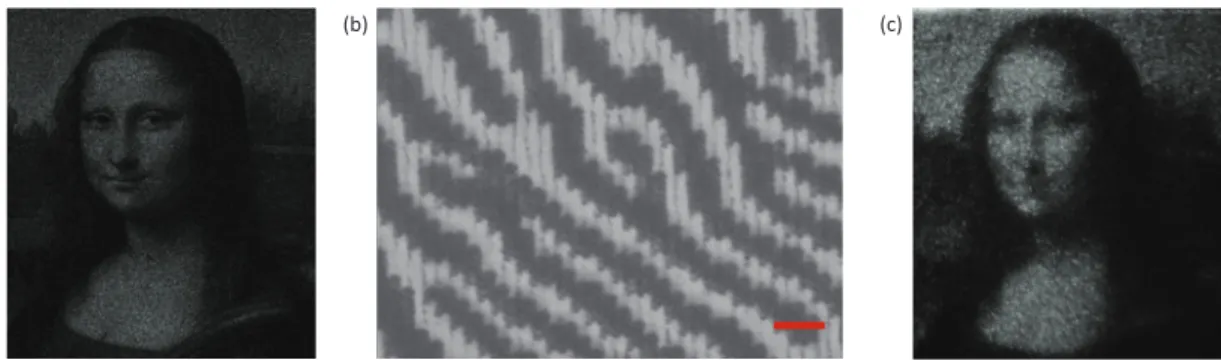
Fig. 1 (a) Simulated holographic image of Mona Lisa. (b) Infrared transmission microscope image of the laser-written phase-type CGH. Dark zones correspond to the processed areas. Scale bar indicates 40μm. (c) Reconstructed image obtained in the far field and captured by infrared camera.
We designed CGHs for Si by using a modified version of the additive-adaptive Iterative Fourier Transform algorithm (IFTA). We customized the spectral condition of adaptive-additive algorithm to obtain phase-type holograms and
STh1Q.7.pdf CLEO:2016 © OSA 2016
expanded the noise space of the iterative generation process to increase the quality of the reconstructed image. These modifications in the algorithm enabled creating CGHs in Si that can produce both binary and grayscale images with binary phase holograms. As a target image the Mona Lisa is chosen. The image width and height are 800 and 600 pixels. These dimensions are also typical for commercial Spatial Light Modulators (SLMs). A representative image of a computer simulation can be seen in Fig. 1(a).
For encoding the holograms, we used a home-built, all-fibre master oscillator power amplifier (MOPA) system that produces 5.5 ns pulses at 300 kHz repetition rate and operates at 1.55μm, where silicon is transparent. During the writing we used 3.3 W of average power and a three-axis motorised stage was used to precisely position the sample with respect to the laser focus. The pixel size is chosen as 10μm after optimization, and pulse energy is kept at 22
μJ/pulse. The microscope image of a portion of the fabricated hologram is shown in Fig. 1(b).
The images are optically reconstructed, with a setup including a Fourier lens, screen and a home-made fiber laser system. We placed a fourier lens 5 cm before the sample to form the image on the focal spot and a diverging lens 15 cm after the sample to have an image large enough to capture. We used the collimated output of the same laser in the processing setup as the illumination source. The reconstructed image with this configuration can be seen Fig. 1(c). Further, we characterized efficiency of the holograms fabricated with our method. We defined efficiency as the power ratio of the first order to zeroth order. We measured efficiency approximately 40 %. We have compared the Si hologram quality with a commercial SLM and observed similar performance in image quality.
In conclusion, the first holograms buried inside silicon were designed and fabricated with a novel approach of non-linear laser lithography. The high resolution, gray-scale reconstructed images are notable for being the first examples of holograms inside Si without damaging the surface. Moreover, the phase-type holograms (kinoforms) demonstrated were not only impossible on Si, but also still not possible on glasses with laser writing, hindering these materials integration into micro-optical applications.
References
1. I.W. Boyd, ”Laser processing of silicon,” Nature 303, 481 (1983)
2. J. Leuthold, C. Koos and W. Freude, ”Nonlinear silicon photonics,” Nature Photon.4, 535 (2010)
3. A. Mouskeftaras, et al. ”Self-limited underdense microplasmas in bulk silicon induced by ultrashort laser pulses,” Appl. Phys. Lett.105, 191103 (2014)
4. O. Tokel, A. Turnali, I. Pavlov, S. Tozburun, I. Akca and F. ¨Omer Ilday , ”Laser-writing in silicon for 3D information processing,” e-print arXiv:1409.2827v1.
5. O. Tokel, A. Turnali, I. Pavlov, F. ¨Omer Ilday , ”Laser writing deep inside silicon for 3D information process-ing,” presented at CLEO/EU-EQEC, Munich, Germany, 21–25 June 2015.
6. O. Tokel, A. Turnali, I. Pavlov, F. ¨Omer Ilday , ”Physical model for subsurface silicon writing,” presented at CLEO-PR, Busan, Korea, 24–28 Aug 2015.
7. A. Turnali, O. Tokel, I. Pavlov, F. ¨Omer Ilday , ”Direct laser writing of volume fresnel zone plates in silicon,” presented at CLEO/EU-EQEC, Munich, Germany, 21–25 June 2015.
8. D. G. Grier, ”A revolution in optical manipulation,” Nature 424, 810 (2003)
9. K. J. Waedegaard and P. Balling, ”High-resolution computer-generated reflection holograms with three-dimensional effects written directly on a silicon surface by a femtosecond laser,” Opt. Exp. 19, 3434 (2011)