LAYER-BY-LAYER SELF-ASSEMBLED
SEMICONDUCTOR NANOCRYSTAL
COMPOSITES WITH NONRADIATIVE
RESONANCE ENERGY TRANSFER FOR
INNOVATIVE ARCHITECTURAL PRECISE
COLOR TUNING AND CONTROL
A THESIS
SUBMITTED TO THE DEPARTMENT OF ELECTRICAL AND ELECTRONICS ENGINEERING
AND THE INSTITUTE OF ENGINEERING AND SCIENCES OF BILKENT UNIVERSITY
IN PARTIAL FULLFILMENT OF THE REQUIREMENTS FOR THE DEGREE OF
MASTER OF SCIENCE
By
Neslihan Çiçek
I certify that I have read this thesis and that in my opinion it is fully adequate, in scope and in quality, as a thesis for the degree of Master of Science.
Assist. Prof. Dr. Hilmi Volkan Demir (Supervisor)
I certify that I have read this thesis and that in my opinion it is fully adequate, in scope and in quality, as a thesis for the degree of Master of Science.
Assist. Prof. Dr. Ali Kemal Okyay
I certify that I have read this thesis and that in my opinion it is fully adequate, in scope and in quality, as a thesis for the degree of Master of Science.
Assist. Prof. Dr. Dönüş Tuncel
Approved for the Institute of Engineering and Sciences:
ABSTRACT
LAYER-BY-LAYER SELF-ASSEMBLED
SEMICONDUCTOR NANOCRYSTAL COMPOSITES
WITH NONRADIATIVE RESONANCE ENERGY
TRANSFER FOR INNOVATIVE ARCHITECTURAL
PRECISE COLOR TUNING AND CONTROL
Neslihan Çiçek
M.S. in Electrical and Electronics Engineering
Supervisor: Assist. Prof. Dr. Hilmi Volkan Demir
August 2009
In recent years semiconductor quantum dot nanocrystals (NC) have attracted significant interest and have found numerous important optoelectronic device applications mainly because of their highly tunable optical properties. For example, precisely tuning shades of color chromaticity is critically important in solid state lighting to achieve ultra-efficient, application-specific, spectrally-engineered illumination. To date such color tuning and control of NC emitters have been investigated and demonstrated only based on their composition, shape, and size (using the quantum confinement effect). All of these parameters are, however, limited to be controlled and set during the synthesis process. As a post-synthesis alternative, we proposed and demonstrated the precise and broad control and tuning of color chromaticity by strongly modifying photoluminescence decay kinetics of NC emitters solely based on nonradiative Förster resonance energy transfer (FRET) in layer-by-layer self-assembled NC composite structures. Locating NC emitters in such a layered architecture with a targeted gradient of bandgap in the close proximity (<10 nm) of each other and spatially interspacing them at the nanoscale (with a precision of <1 nm) enabled us to fine-tune and master FRET at a desired efficiency level of nonradiative energy transfer from electronically excited donor NCs to luminescent acceptor
NCs. These proof-of-concept experimental demonstrations, combined with our numerical modeling and simulation results, proved a highly sensitive tuning capability based on FRET to span a broad color area in Commission Internationale De L’Eclairage (CIE) chromaticity diagram in principle beyond the limits of each of the commonly used LED epitaxial material systems. This innovative architectural tuning opens up a new direction for the photometric engineering of color-conversion LEDs.
Keywords: semiconductor nanocrystals, quantum dots, nonradiative Förster resonance energy transfer, layer-by-layer assembly, self-assembly.
ÖZET
TABAKA TABAKA DİZİLMİŞ YARIİLETKEN
NANOKRİSTAL KOMPOZİTLERDE FÖRSTER
REZONANS ENERJİ TRANSFERİ İLE MİMARİ
OLARAK HASSAS YENİLİKÇİ RENK AYARLANMASI
VE KONTROLÜ
Neslihan Çiçek
Elektrik Elektronik Mühendisliği Yüksek Lisans Tez Yöneticisi: Yard. Doç. Dr. Hilmi Volkan Demir
Ağustos 2009
Son yıllarda yarıiletken kuvantum noktacık nanokristaller büyük bir ilgi toplamıştır. Bu nanokristaller, optiksel özelliklerinin ayarlanabilir olmasından dolayı pek çok optoelektronik aygıtta uygulama alanı bulmuşlardır. Örneğin, renk tonlarının dar toleransla ayarlanabiliyor olması, katı hal tabanlı aydınlatmalarda yüksek verimli, ışıma tayfı değiştirilebilir ve uygulamaya özel ışıklandırma için büyük önem taşımaktadır. Bugüne kadar nanokristal ışıyıcıların renklerinin ayarlanması ve kontrolü ise sadece nanokristallerin kimyasal içeriklerine, şekillerine ve büyüklüklerine bağlı olarak (kuvantum sınırlandırma etkisi kullanılarak) incelenmiş ve gösterilmiştir. Ancak bu parametreler sadece sentez sırasında kontrol edilip ayarlanabilmektedir. Bu tez çalışmasında, sentez sonrası için bir alternatif olarak, sadece Förster rezonans enerji transferi (FRET) yardımıyla tabaka-tabaka kendiliğinden dizilme tekniğiyle yapılandırılmış nanokristal ışıyıcıların fotoışıma kinetikleri değiştirilerek, renklerinin hassas bir şekilde geniş bir tayfta kontrol edilip ayarlanması önerilmiş ve gösterilmiştir. Aralarında yasak bant farkı bulunan
nanokristal ışıyıcılarını birbirine 10 nm’den yakın uzaklıkta tabakalı bir mimaride yerleştirebilmek ve bu nanokristaller arasındaki uzaklığı 1 nm’den daha az bir hassasiyette değiştirebilmek, elektronik olarak uyarılmış verici nanokristallerin ışıyan alıcı nanokristallere ışıma yapmadan FRET’le aktardığı enerjinin miktarını (ve verimliliğini) istediğimiz seviyede ayarlayabilme olanağını sağlamıştır. Bu önerinin doğruluğunu göstermek amaçlı yapılmış olan deneylerimiz, sayısal modellemelerimiz ve simulasyon sonuçlarımız ile beraber, nanokristaller arasında FRET kullanılarak, yaygın olarak kullanılan LED epitaksiyel materyal sistemlerinin her birinin ayrı ayrı limitlerinin de ötesinde, prensipte CIE kromatisite diyagramında son derece hassas renk ayarlamasının geniş bir alanı kapsadığını kanıtlamıştır. Bu mimari yenilikçi yaklaşım renk-dönüştürme LED’lerinin fotometrik mühendislikleri için yeni bir yol açmaktadır.
Anahtar kelimeler: Yarıiletken nanokristaller, kuvantum noktacıklar, Förster rezonans enerji transferi, tabaka-tabaka dizilme, kendiliğinden dizilme.
Acknowledgements
First of all, I would like to express my sincere gratitude to Prof. Hilmi Volkan Demir who gave me a chance to work with him. He has always been a kind and motivating advisor and without his invaluable guidance, suggestions, and endless support, I could not finish this study.
I would like to thank the members of the thesis committee, Prof. Ali Kemal Okyay, and Prof. Dönüş Tuncel for reading and commenting on the thesis.
I especially thank and acknowledge my dear friend, Aslı Ünlügedik for many reasons. She was always with me whenever I need her. I would like to thank her incredible amount of patience she had with me in the last two years.
I thank all of my friends for their friendship throughout all these years, a partial list of them being Gülis Zengin, Can Uran, Sevinc Figen Oktem, Ezgi Arslan, Hakan Arslan, Refik Sina Toru, Mustafa Akın Sefünç, Elif Aydoğdu with whom I enjoyed life in Bilkent. I want to take this opportunity to express my thanks to all of them.
I would like to express my special thanks to all of my friends in Demir group at Bilkent.
I would like to acknowledge TUBITAK for their support during my MS studies. Last but not least, it is a pleasure to express my special thanks to my father, my mother, my sister Tuğba and her husband Yaşar, and my sister Nagihan for their constant support, patience, and sincere love.
Table of Contents
1. INTRODUCTION ... 1
2. OVERVIEW OF COLLOIDAL SEMICONDUCTOR NANOCRYSTAL QUANTUM DOTS AND THEIR APPLICATIONS ... 4
2.1BACKGROUND ON COLLOIDAL SEMICONDUCTOR NANOCRYSTALS .. 4
2.1.1 Fundamental properties of semiconductor nanocrystals ... 4
2.1.2 Properties and specifications of different II-IV semiconductor nanocrystals ... 6
2.2APPLICATIONS OF SEMICONDUCTOR NANOCRYSTALS... 6
2.2.1 Biolabeling and bioimaging ... 7
2.2.2 Optoelectronic devices ... 8
2.2.2.1 Light emitting diodes (LEDs) ... 8
2.2.2.2 Solar cells ... 9
2.2.2.3 Sensors ... 10
2.3WATER-SOLUBLE COLLOIDAL CDTE ... SEMICONDUCTOR NANOCRYSTAL SYNTHESIS ... 11
3. OVERVIEW OF LAYER-BY-LAYER ASSEMBLY OF MULTILAYER THIN FILMS AND APPLICATIONS ... 15
3.1BACKGROUND ON LAYER-BY-LAYER ASSEMBLY OF MULTILAYER THIN FILMS ... 15
3.1.1 Layer-by-layer assembly ... 15
3.1.2 Applications of layer-by-layer assembly ... 16
3.1.2.1 Sensor applications ... 16
3.1.2.2 Polymer-integrated electronic devices ... 17
3.1.2.3 Assembly of nanotubes ... 18
3.1.3 Film preparation with layer-by-layer assembly of CdTe nanocrystals ... 19
3.2LAYER-BY-LAYER ASSEMBLY FOR PRECISE TUNING ... 20
3.3LAYER-BY-LAYER ASSEMBLY FOR BROAD TUNING ... 24
4.1BACKGROUND ON FÖRSTER RESONANCE ENERGY TRANSFER ... 25
4.1.1 Characteristics of Förster resonance energy transfer... 25
4.2APPLICATIONS OF FÖRSTER RESONANCE ENERGY TRANSFER ... 31
4.2.1 Molecular distance measurements ... 32
4.2.2 Sensor applications ... 33
4.2.3 Nanocrystal embedded optoelectronic devices ... 35
5. LAYER-BY-LAYER SELF-ASSEMBLED SEMICONDUCTOR NANOCRYSTAL COMPOSITES WITH NONRADIATIVE RESONANCE ENERGY TRANSFER FOR INNOVATIVE ARCHITECTURAL PRECISE COLOR TUNING AND CONTROL ... 37
5.1PRECISE TUNING OF COLOR CHROMATICITY ... 37
5.1.1 Motivation ... 37
5.1.2 Experimental work ... 38
5.1.3 Characterization ... 40
5.1.4 Theoretical analysis ... 46
5.2BROAD TUNING OF COLOR CHROMATICITY ... 48
5.2.1 Motivation ... 48
5.2.2 Experimental work ... 49
5.2.3 Characterization ... 50
6. CONCLUSION AND FUTURE PROSPECTS ... 56
6.1CONCLUSION ... 56
6.2FUTURE PROSPECTS ... 57
6.2.1 Cascaded Förster resonance energy transfer between NCs for broad tuning of color chromaticity ... 57
7. BIBLIOGRAPHY ... 60
8. APPENDIX ... 69
MATLAB CODE FOR FÖRSTER RADIUS CALCULATION ... 69
MATLAB CODE FOR MODELLING CASCADED FÖRSTER RESONANCE ENERGY TRANSFER ... 71
List of Figures
Figure 2.1.1.1 Energy states for bulk and quantum dot semiconductor ...5 Figure 2.3.1 Apparatus of water-soluble CdTe semiconductor nanocrystals synthesis...12 Figure 2.3.2 Red-brown mixture after the formation of CdTe nanocrystals...13 Figure 2.3.3 Absorption spectra of fractions of CdTe NCs in solution...13 Figure 2.3.4 Normalized photoluminescence spectra of fractions of CdTe NCs in solution………....14 Figure 3.1.2.2.1 Schematic diagram of the layer-by-layer polymer-integrated field effect transistor...18 Figure 3.1.2.1 Scheme of the layer-by-layer assembly method for thin film construction of polymer-nanocrystal bilayers ...19 Figure 3.2.1 Multi-vessel dip coater (Nima Technology) at Demir Lab at Bilkent...21 Figure 3.2.2 Cross-sectional sketch of layer-by-layer spaced, donor-acceptor paired CdTe nanocrystal solids with a controlled spacing between the donor and acceptor monolayes...22 Figure 3.2.3 Focused ion beam etched cross-section of 20 bilayers of PAA-PSS films...23 Figure 3.2.4 Focused ion beam etched cross-section of 10 bilayers of PAA-NC films...23 Figure 4.1.1.1 Schematic representation of the spectral overlap between donor molecule emission spectrum and acceptor molecule absorption spectrum...27 Figure 4.1.1.2 Schematic diagram for the demonstration of effect of donor-acceptor separation on Förster resonance energy transfer rate... 30 Figure 4.1.1.3 Jablonski diagram for FRET………31
Figure 4.2.1.1 Biolabeling of melittin peptide to measure the distance between two sides...32 Figure 4.2.2.1 Schematic diagram for monitoring telomerization and DNA replication using FRET...33 Figure 4.2.2.2 Schematic diagram for sensing K+ ions using FRET between
donor and acceptor NCs...34 Figure 4.2.3.1 Sketch of a device structure with alternating nanocrystal monolayers and its staircase like bandgap profile...35 Figure 5.1.2.1 Absorption spectrum of CdTe NCs in solution (with an absorption exciton peak @ 612 nm) and that of dye rhodamine 6G...39 Figure 5.1.2.2 Emission spectrum of CdTe NCs in solution (with an emission peak @ 640 nm) and that of dye rhodamine 6G, taken using an excitation source at a wavelength of 467 nm...40 Figure 5.1.3.1 Time-resolved PL decays of donor and acceptor CdTe NCs that are spaced using 1 ML, 3 ML, and 5 ML polyelectrolyte at the donor peak emission wavelength of 595 nm and at the acceptor peak emission wavelength of 645 nm along with steady-state PL spectra of these samples of only donor, only acceptor, and controllably spaced donor-acceptor ...42 Figure 5.1.3.2 Absorption spectra of only donor, only acceptor, and controllably spaced donor-acceptor samples. ...44 Figure 5.1.4.1 Commission Internationale De L’Eclairage (CIE) chromaticity diagram for tuning chromaticity coordinates in our LbL spaced NC samples and their semiempirical analytical model for color tuning based on FRET efficiency along with the experimental results………...……...47 Figure 5.2.3.1 Time-resolved PL decays of donor and acceptor CdTe NCs that are spaced with 1 ML, 3 ML, and 5 ML polyelectrolyte at the donor peak emission energy of 2.23 eV and at the acceptor peak emission energy of 1.92 eV………...51 Figure 5.2.3.2 CIE chromaticity diagram for tuning chromaticity coordinates of our LbL spaced NC samples integrated with an isolated blue emitter of polyfluorene...52
Figure 5.2.3.3 CIE chromaticity diagram for tuning chromaticity coordinates of our LbL spaced NC samples integrated with an isolated blue emitter of CdSe/ZnS NCs... 53 Figure 5.2.3.4 Semi-empirical analytical model simulation results for color tuning based on FRET efficiency along with the experimental results for x chromaticity coordinate...54 Figure 5.2.3.5 Semi-empirical analytical model simulation results for color tuning based on FRET efficiency along with the experimental results for y chromaticity coordinate...55 Figure 6.2.1.1 CIE chromaticity diagram for tuning chromaticity coordinates in our model.………...58 Figure 6.2.1.2 Steady state photoluminescence spectra of our one monolayer spaced sample...59
List of Tables
Table 5.1.3.1 Average decay lifetimes, spectrally integrated relative total emission and FRET efficiencies of our LbL spaced donor-acceptor NC samples along with their control groups...43 Table 5.1.3.2 Scaling coefficients for the normalization of steady state measurements...44
Chapter 1
Introduction
Precisely tuning shades of color chromaticity is critically important in solid state lighting particularly to achieve application specific spectral illumination (e.g., for indoors applications). For this purpose, colloidal semiconductor nanocrystals (NCs) are essentially advantageous with their highly tunable optical properties. Such color tuning of semiconductor quantum dots is commonly enabled via changing their composition, shape, and size (based on the quantum confinement effect) [1]. However, all of these parameters are controlled and set conventionally during the synthesis process. In this thesis, as a post-synthesis alternative to these, we propose and demonstrate the control of nonradiative Förster resonance energy transfer (FRET) in NC emitters by constructing their layer-by-layer (LbL) assembled composite films to conveniently tune their collective color, after their synthesis while keeping the type, composition and shape of NCs fixed. This structural control of LbL constructs enables a post-synthesis color tuning capability, alternative or additive to using the size, shape, and composition of nanocrystals.
In the second chapter of this thesis, an overview of fundamental material properties of colloidal semiconductor nanocrystals is explained and different specifications of important II-IV semiconductor nanocrystals are described. For examples of application, the use of NCs in biolabeling and bioimaging with the help of their surface functionalization and nanocrystal based optoelectronic devices including light emitting diodes, sensors and solar cells are introduced.
Furthermore, the synthesis of colloidal negatively charged water soluble CdTe semiconductor NCs (which is applied in our group) is described as a general background and the optical properties of these NCs are discussed.
In the third chapter, the attractive features of LbL assembly technique, which allows for forming uniform and multicomponent thin films consisting of functional molecules and nanocrystals, are presented. The flexibility of applying this technique to different substrates, surfaces or devices, combined with the flexibility of chosing different LbL construction elements broadens possible application areas. A wide range of LbL assembly applicatons is subsequently illustrated in this chapter. Finally, LbL film formation of water soluble semiconductor NCs is explained.
In the fourth chapter, nonradiative Förster resonance energy transfer is presented as a spectroscopic process by which energy is transferred nonradiatively from the donor molecule in the excited state to the acceptor molecule in the ground state in a close proximity (i.e., < 10 nm) as a result of long-range dipole-dipole interactions. Förster radius, Förster energy transfer rate, and Förster efficiency are introduced in this chapter. Moreover, different application areas of FRET including molecular distance meaurements, sensors, and NC embedded electronic devices are given as examples.
In the fifth chapter, we present architectural fine-tuning of color chromaticity by controlling radiative decay kinetics through nonradiative Förster resonance energy transfer in the heterostructure of layer-by-layer spaced CdTe nanocrystal solids. We demonstrate highly sensitive tuning by precisely adjusting the Förster energy transfer efficiency from donor nanocrystal monolayers to acceptor nanocrystal monolayers via controlling nanocrystal separation at the nanoscale with the help of layer-by-layer assembly technique. Also, we present light emitting heterostructures with a reproducible and efficient spectrum, which is broadly tunable across the CIE (Commission Internationale de l’Eclairage) color
space, generated by a Förster resonance energy transfer pair of green and red emitting NC monolayers and isolated blue NC monolayer.
In the last chapter, the conclusions of this thesis and future prospects of our work are presented.
Chapter 2
Overview of colloidal semiconductor
nanocrystal quantum dots and their
applications
2.1 Background on colloidal semiconductor
nanocrystals
2.1.1 Fundamental properties of semiconductor
nanocrystals
For semiconductors the bandgap energy that separates the conduction band and the valence band is one of the most essential parameters and for bulk semiconductors this parameter is almost fixed. However, for nanoscale semiconductor based particles, nanocrystals, which are strongly confined in all three dimensions (less than 10 nm), this situation changes [1]. Within this size range electronic excitations respond to size changes, which adjust their energy spectra. This is known as quantum confinement effect and this leads to larger separation of energetic levels (Figure 2.1.1.1).
Figure 2.1.1.1 (a) A bulk semiconductor has continuous conduction and valence bands separated by a fixed bandgap whereas (b) a quantum dot has discrete energy states [2].
The bandgap of NCs can be modified by varying their sizes, which gives rise to unique size dependent optical properties. When the particle becomes smaller and smaller its emission is more and more blue shifted. Conversely, larger particle size leads to red shift in the emission spectra. This allows for the coverage of large spectra by using the same material.
Quantum dots also feature narrow emission spectra (full-width-half-maximum about 30 nm), broad absorption profiles, and high extinction coefficients.
2.1.2 Properties and specifications of different
II-IV semiconductor nanocrystals
Among the most important group II-IV semiconductor nanocrystals, which have attracted interest in material research, are:
Cadmium Telluride (CdTe) Quantum Dots: CdTe quantum dots can be
synthesized both as negatively and positively charged as desired in water soluble form with narrow emission spectra with the widest emission wavelength tuning range (500 - 740 nm) [3].
Cadmium Selenide/Zinc Sulfide (CdSe/ZnS) Quantum Dots: CdSe/ZnS
quantum dots are core-shell nanocrystals in which an inner core part of cadmium selenide (with a bandgap of 1.74 eV) is encapsulated with a shell of wider band gap (3.7 eV) zinc sulfide. In order to overcome lattice mismatch between CdSe and ZnS an intermediate adapter can be used, e.g., CdS. CdSe/ZnS nanocrystals emit at wavelengths ranging from 520 to 620 nm [4].
Lead Selenide (PbSe) quantum dots: PbSe quantum dots emit at infrared
wavelengths and they have found application in infrared detectors for thermal imaging and in photovoltaic semiconductors for solar energy applications [5].
2.2 Applications of semiconductor nanocrystals
To achieve small and more efficient devices it is important for scientists and engineers to come up with new materials that allow the development of new
semiconductor nanocrystals have attracted considerable interest with their tunable optical absorption and emission spectra, which are a function of their size [6]. Therefore, an optoelectronic device whose working principle relies on optical absorption and emission mechanisms can utilize nanocrystals embedded in them in principle. Also, nanocrystals can be functionalized with surface modifications and this property further broadens the application areas of these nanocrystals.
2.2.1 Biolabeling and bioimaging
Biolabeling is defined as inserting a marking element into a biological specimen to track changes that occur in the biological environment. The role of the inserted marker is to emit light which can be detected when the sample is excited. Nanocrystals were first reported as a very promising tool for cellular imaging by Allivisatos in 1998 [7]. As it is explained by Bruchez et al., nanocrystals have several advantages compared to dye fluorophores; e.g., nanocrystals have broad absorption spectrum and all the colors inside a sample can be excited using a single laser source. Then, if several nanocrystals are used as marking agents in the same specimen, then all the biolabels inside a sample may be excited simultaneously.
Furthermore, the emission spectrum of nanocrystals is narrower and hence their spectral overlap with other colors is negligible. Using this advantage, several colors can be safely detected simultaneously. Nanocrystals have also high quantum efficiencies comparable with the conventional dyes. Moreover, they are stable and can absorb much more light than dyes. These stability and brightness properties may allow observing rare molecules inside biological samples using NCs, which are otherwise unobservable with conventional dyes [8].
On the other hand, despite the significant advantages of NCs over organic dyes, biolabeling with NCs was not possible because of their insolubility in water. This obstacle was overcome by changing the surface chemistry of CdSe NCs. The use of mercaptoacetic acid to cap the surface of CdSe/ZnS NCs to make them soluble in aqueous media is proposed and demonstrated [9].
Toxicity of NCs is also an important concern for detection of biological processes in vivo experiments. However, most studies report no toxicity in live animals, even in embryos under standard conditions [10]. Oxidation of CdSe can cause Cd+ to be released, which is then toxic to living cells, and hence NCs should be protected from oxidation.
2.2.2 Optoelectronic devices
2.2.2.1 Light emitting diodes (LEDs)
Semiconductor nanocrystals have attracted considerable interest with their highly tunable optical properties and have been exploited in various color conversion light emitting diode (LED) applications [11-16].
Conventional LEDs are fabricated to emit at a particular wavelength and by using conventional materials it is not possible to produce all wavelengths across a large spectral region. The nanocrystals offer flexibility in selecting and tuning the emission wavelength of the device. Semiconductor nanocrystals can be manufactured in high quality in reasonable volumes and different NCs to emit in the wavelength range of 400 to 2000 nm. Further advantages of some of
nanocrystal-based devices are that they may consume relatively little energy and their small sizes may also allow them to be incorporated into many devices.
2.2.2.2 Solar cells
Around the world fuel energy sources become scarcer. The environmentally destructive emission during their consumption forces us to look for non-polluting and renewable energy production methods. Among these energy generation methods, the sun is the most important energy source.
Solar cells are devices that convert solar light directly into electricity by the photovoltaic effect. However, photovoltaic energy has not yet proven as cost effective as its potential since the materials utilized in the manufacture of photovoltaic devices are expensive. The cost of nanocrystals is lower compared with the conventional highly ordered solar cell materials and this may make such solar devices possibly economical [17].
Quantum dots offer several advantages including extending the bandgap of a solar cell and increasing the possibility of confining more of the incident light in the solar spectrum. When the bandgap of a solar cell widens, the output voltage that is generated enhances. On the other hand, when the bandgap becomes smaller the produced current increases. For efficient solar energy to electrical energy conversion both high currents and high voltages are required. The capability of tuning the bandgap of the solar cells using nanocrystals gives an advantage of operating with optimum bandgap which promotes the efficiency of the device.
So far, several studies and designs have been reported for solar cells involving nanocrystals [18,19]. In Ref. 18, NC incorporated solar cells have been
investigated for the purpose of improving the efficiency of solar cells in which NCs were used in the active region to capture a large percentage of the incident solar light and to accumulate the resulting photo generated current. In these devices, solar cell efficiency has been increased as a result of multiple exciton generation. Further, in Ref. 20, a hybrid solar cell which includes polymer and nanorods has been revealed and in this study different nanoparticle sizes have been utilized to analyze their effect on the efficiency of the device.
2.2.2.3 Sensors
The utility of NCs has been expanded for their use in optical sensors and initial applications were based on physical sensing. The photoluminescence characteristics of CdSe/ZnS NCs strongly depend on temperature and this property were employed to develop a temperature probe [21].
Moreover, nanocrystals have a large surface to volume ratio and this attribute allows for the detection of certain chemical targets existing in the environment. When the target species interact with the nanocrystal receptor, NC luminescence is perturbed by the presence of a specific target analyte. In some cases, the fluorescence intensity is decreased by morphological changes on the lattice. For instance, Ag+, Pb2+, and Cu2+ ions quench NC luminescence by replacing the
Cd2+ ions in the nanocrystal lattice [22]. By injecting excess Cd2+ to the NC
environment luminescence can be recovered. However, since this is not practical for sensing purposes detection of specific target analytes has been achieved reversibly using CdSe NCs with modified surfaces [23].
2.3 Water-soluble colloidal CdTe
semiconductor nanocrystal synthesis
Here, the synthesis methodology for negatively charged colloidal CdTe nanocrystals stabilized with thioglicolic acid described by N. Gaponik et al. is presented as an example [24,25]. In a typical synthesis procedure 4.59 g of Cd(ClO4)2x6H2O is dissolved in 0.5l of Milli-Q water in a 1l three-neck reaction
flask. Slowly addition of 1.33 g thioglycolic acid (TGA) leads to a milky mixture. The pH of this mixture is increased to 11.8 – 12.0 by drop wise addition of NaOH upon vigorous stirring. After this step the reaction mixture becomes clear or slightly turbid (Figure 2.3.1). To prepare tellurium precursor 0.82 g of Al2Te3 is transferred into a small three-neck flask in the glove box. A
setup identical to that in Ref. 24 is assembled and deaerated by passing Ar for 50 min. 10 ml of deaerated 0.5M H2SO4 is slowly poured onto Al2Te3 lumps and
the produced H2Te gas, carried by a slow Ar flow, is bubbled through the
Figure 2.3.1 Apparatus of water-soluble CdTe semiconductor nanocrystals synthesis. After the regulation of pH to 11.8-12.0 solution becomes slightly turbid and clear (with our Phoremost
collaborators).
The resulting red-black mixture (Figure 2.3.2) is refluxed at 100°C for 2 min to obtain CdTe NCs that emit at 535 nm, 3 hours to obtain CdTe NCs that emit at 595 nm, for 21 hours to obtain CdTe NCs that emit at 640 nm (Figure 2.3.3-2.3.4). These durations are determined by taking small amounts of samples from the CdTe mixture and by checking their absorption and emission spectra.
Figure 2.3.2 Red-brown mixture after the formation of CdTe nanocrystals (with our Phoremost collaborators). 400 500 600 700 800 0.00 0.02 0.04 0.06 Ab s o rpt ion Wavelength (nm)
CdTe NCs abs. max @ 510 nm CdTe NCs abs. max @ 560 nm CdTe NCs abs. max @ 612 nm
500 550 600 650 0.0 0.2 0.4 0.6 0.8 1.0 Ph o to lu m in esce n ce In tensity (a.u .) Wavelength (nm) CdTe NCs emm. max @ 535 nm CdTe NCs emm. max @ 595 nm CdTe NCs emm. max @ 640 nm
Figure 2.3.4 Normalized photoluminescence spectra of fractions of CdTe NCs in solution.
Subsequently, the reaction mixture is quickly cooled down to room temperature and then filtered. CdTe NCs are separated by the size selective precipitation, through adding isopropanol and centrifuging the mixture at 4500 rpm for 3 min. The precipitated solution that remains on the bottom are the biggest NCs and the solution on the top is the stock solution that contains differently sized nanorystals to continue size selective precipitation procedure. Then, for cleaning from residues, the precipitated large NCs are separated, water is added, and the mixture is again centrifuged one more time at 13,400 rpm for 5 min. After the centrifuging step, the dispersion on top is water-soluble CdTe NCs with the largest diameter. This whole procedure is repeated until the solution which contains nanocrystals with different sizes inside becomes transparent. According to the size curve in Ref. 25 the average particle diameters are estimated to be 2.6, 2.9, and 3.7 nm for the CdTe NCs using this recipe.
Chapter 3
Overview of layer-by-layer assembly
of multilayer thin films and
applications
3.1 Background on layer-by-layer assembly of
multilayer thin films
3.1.1 Layer-by-layer assembly
Layer-by-layer assembly, which was first proposed for the assembly of polyelectrolytes, is a well-known simple fabrication technique for the arrangement of multi-layered micro-nano scale structures with desired electrical and optical properties [26,27]. There are many advantages of this layer-by-layer (LbL) assembly technique including simplicity, versatility, and thickness control in nanoscale precision. Besides, the most attractive property of LbL assembly is that it does not require highly purity components or sophisticated hardware; it is a low cost technique. For most of the aqueous-soluble and charged elements, it is easy to find an LbL pair to build thin films and the variety of components is
available to construct LbL films. The multilayer thin films may show unique properties, which are not present in construction elements.
The main idea of LbL assembly is to obtain multilayered thin film structures by linking the desired oppositely charged materials through alternatively dipping into their respective solutions. After each adsorption step the excess solution on the sample is rinsed with water and thus a clean monolayer (or a sub-monolayer) of charged species on the surface is produced. Multilayer films on an arbitrarily shaped substrate can also be coated by using LbL assembly technique.
3.1.2 Applications of layer-by-layer assembly
The attractive features of LbL deposition technique have provided a road to the large number of organic–inorganic heterostructures which can contain functional groups to improve the properties of the composites. Using such heterostructures multidimensional devices have been created.
3.1.2.1 Sensor applications
Layer-by-layer deposition technique is one of the most common techniques for molecular sensing applications. For example, layer-by-layer assembly was employed for deposition of TiO2 nanoshells and biocompatible films were
constructed with this technique [28]. In this study titania spheres were synthesized by removing Ag cores inside Ag-TiO2 core-shell structures. After
selective response when the pH of the environment changes even by small amounts. By using this feature of LbL assembled TiO2 nanoshells studies were
conducted for sensing dopamine hormone, which is one of the fundamental neurotransmitter in the human body, and highly sensitive promising results were demonstrated.
Moreover, by alternating layer-by-layer sequential adsorption of polyelectrolytes poly(allylamine) hydrochloride (PAH) and poly(anilinesulfonic acid) polymer-based ultra-thin humidity sensors have been fabricated [29]. To compare the performances of humidity sensors fabricated using spin coating and layer-by-layer assembly techniques, the change in the humidity-dependent resistance of the latter sensor was measured as 11% while the former sensors was 6% in response to change in the relative humidity. Therefore, layer-by-layer deposited humidity sensors exhibit much more sensitive and reliable results compared to the spin coated sensors.
3.1.2.2 Polymer-integrated electronic devices
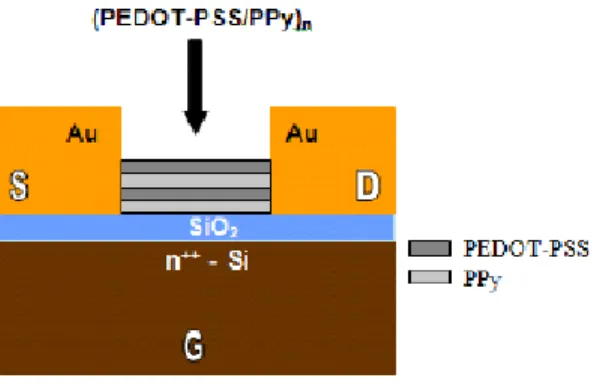
Several polymer-based electronic devices have been explored including light emitting diodes and transistors by using layer-by-layer assembly [30]. Khillan et al. applied LbL assembly with alternating layers of poly(3,4-ethylenedioxythiophene)-poly(styrenesulfonate) (PEDOT-PSS) and polypyrrole (PPy) between the source and drain for the realization of polymer heterostructure-based field effect transistors (Figure 3.1.2.2.1). The conducting layer-by-layer assembled PEDOT-PSS/PPy film facilitates the confinement of holes and enhances the possibility of recombination at the electroluminescent part and hence improves the device performance.
Figure 3.1.2.2.1 Schematic diagram of the layer-by-layer polymer-integrated field effect transistor.
3.1.2.3 Assembly of nanotubes
As the traditional lithography reaches its limits the assembly of nanotubes with layer-by-layer deposition technique has gained importance [31]. For example, carbon nanotube layer-by-layer assemblies, which feature high conductivity and capacitance, can easily be constructed [32]. In this work, growth of multilayer films shows pH dependence and by adjusting the pH levels nanopores can be constructed, which is a desired property for various electrochemical applications.
3.1.3 Film preparation with layer-by-layer
assembly of CdTe nanocrystals
A number of different techniques have been known for the fabrication of ordered nanocrystal based devices including self-organization and crystallization [33,34]. Among these techniques layer-by layer assembly becomes one of the widely used methods because of the desirable properties that are discussed above.
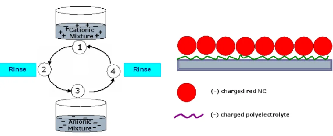
Before layer-by-layer assembly, a corning glass substrate is cleaned with acetone in ultrasonic bath for 30 min and to have a surface with negative charge it is put into the NaCl solution overnight. A standard cyclic approach that is employed for CdTe NC film preparation on solid substrates is described in the following procedure to form a polymer/ nanocrystal bilayer (Figure 3.1.2.1).
Figure 3.1.2.1 Scheme of the layer-by-layer assembly method for thin film construction of polymer-nanocrystal bilayers.
1) Substrate is firstly dipped into a solution of positively charged linker polymer.
2) As an intermediate step, substrate is subsequently rinsed with water (Milli-Q) to remove residues on the surface.
3) Substrate is then dipped into aqueous dispersion of negatively charged CdTe NCs.
4) Finally it is rinsed with water again.
When this procedure is completed in this circle a bilayer of polymer/nanocrystal composite illustrated in Fig. 3.1.2.1 is obtained.
3.2 Layer-by-layer assembly for precise tuning
To make artificial nanocrystal solids with controllably spaced nanocrystal monolayers (ML) in layer-by-layer assembly, water-soluble negatively charged CdTe nanocrystals stabilized with thioglycolic acid were used.
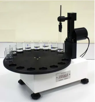
In the LbL assembly of these nanocrystals, positively charged polymer poly (allylamine) (PAA) and negatively charged polymer poly (styrene sulfonate) (PSS) were used as linkers. Their working concentrations were 2 mg ml-1 of PSS and 0.5% of PAA, both in 0.1 M NaCl. For the multilayer LbL construction, a computer controlled multi-vessel dip coater (Nima Technology) shown in Fig. 3.2.1 was employed. To form a NC ML, the substrate was dipped into an aqueous solution of negatively charged CdTe NCs (with the smaller size 2.9 nm to serve as donors or with the larger size 3.7 nm as acceptors), both with a particle concentration of 1.3 µM in 0.1 M NaCl for 10 min, and then it was rinsed in purified water for 2 min.
Figure 3.2.1 Multi-vessel dip coater (Nima Technology) at Demir Lab at Bilkent.
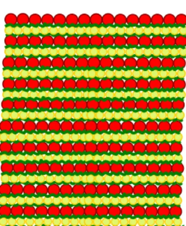
To construct polyelectrolyte interspacing of a desired thickness, multiple monolayers of PAA and PSS films were consecutively formed in alternating order by dipping in their respective solutions for 10 min and rinsing in water for 2 min and repeating this sequence as many times as required. A similar approach of controlled interspacing was also previously utilized for plasmonic coupling in the work of Kulakovich et al. [35]. In our implementation, the heterostructure unit of spacer-NC-spacer-NC was repeated for 10 times to complete the entire three-dimensional layered construction of each sample as illustrated in Fig. 3.2.2.
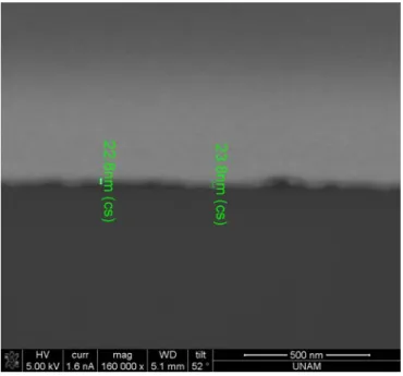
In the repeating unit between NC MLs, only PAA was used for 1 ML interspacing; then PSS-PAA, for 3 MLs interspacing; and finally PAA-PSS-PAA-PSS-PAA, for 5 MLs interspacing. According to our focused ion beam (FIB) etched cross-section as shown in Fig. 3.2.3, 20 bilayers of PAA and PSS gives approximately a film thickness of 23 nm. This implies that a single
polymer ML provides a thickness of ~0.6 nm. Also, as it is shown in Fig. 3.2.4, 10 bilayers of PAA and NC gives 45 nm thickness. It is known that the NC diameter is 3.7 nm, hence the surface capping of NCs effectively provides ~0.2 nm in the film thickness.
Figure 3.2.2 Cross-sectional sketch of layer-by-layer spaced, donor-acceptor paired CdTe nanocrystal solids with a controlled spacing between the donor and acceptor monolayes.
Therefore, our NC MLs are spaced approximately 1.0, 2.2 and 3.4 nm apart from each other for 1, 3 and 5 MLs of polyelectrolyte spacing, respectively. For our control samples we also fabricated only donor NCs and only acceptor NCs.
Figure 3.2.3 Focused ion beam etched cross-section of 20 bilayers of PAA-PSS films.
3.3 Layer-by-layer assembly for broad tuning
We fabricate different multilayer structures consisting of two differently sized CdTe NCs with different interspacings, which are similar to those structures described in Section 3.2. In the layer-by-layer assembly of CdTe NCs and spacer layer polymers (the positively charged poly(diallyl dimethylammonium) chloride (PDDA) and negatively charged polymer poly (styrene sulfonate) (PSS) dispersions), the same concentrations and process durations are employed as in Section 3.2. The resulting heterostructure contains 10 sets of bilayers that are composed of three main blocks: the monolayer of large NCs (acceptor), the spacer layer PDDA/(PSS/PDDA)n where (PSS/PDDA)n denotes n sets of
bilayers of PDDA and PSS, and the monolayer of small NCs (donor). To generate a broad spectral emission, an isolated drop-casted blue emitting NC is integrated to the FRET pair of green and red emitting NC monolayers. To demonstrate spectral tunability, we adjust the relative concentration of NC component in the blue emitter. Therefore, independent processing of NC FRET pair and the isolated NC layer allows for precise and broad tuning of the emission spectrum without changing the device structure. Also for various tones of color generations, in addition to NC luminophores a blue emitting polyflourene is utilized as a replacement for isolated NC color component and different fractions of this polymer are applied.
Chapter 4
Overview of Förster resonance
energy transfer and its applications
4.1 Background on Förster resonance energy
transfer
4.1.1 Characteristics of Förster resonance energy
transfer
Förster resonance energy transfer (FRET) is defined as a spectroscopic process by which energy is transferred nonradiatively from the donor molecule in the excited state to the acceptor molecule in the ground state over the distances of 1 to 10 nm as a result of long-range dipole-dipole interactions [36]. Typically donor molecule has a wider bandgap (hence it emits at shorter wavelengths) and the acceptor molecule has a narrower bandgap (thus it emits at longer wavelengths). The transfer does not involve photons as the excitation energy is transferred nonradiatively. The energy transfer rate strongly depends on the separation distance between the donor and acceptor molecules, the spectral overlap integral between the donor molecule emission and acceptor molecule
absorption spectra, the relative orientation of the donor and the acceptor dipoles. At the distance of Förster radius, which is given by [1]
6 / 1 4 0 0.211(κ n Q J(λ)) R = 2 − D (1)
the FRET efficiency drops to its 50% of its maximum at zero distance. The typical Förster radius R0 is around 3-4 nm.
In this formula κ2 is the dipole orientation factor (taken to be 2/3 for random orientation), n is the refraction index of the intermediate medium, QD is the
quantum efficiency of the donor, and J (λ) is the spectral overlap integral. Therefore, all of these factors must be known to calculate the Förster radius. The refractive index is generally known from the solvent composition or it can better be measured on thin films by using ellipsometer. The quantum yield of the donor is determined by comparison with standard dyes. The overlap integral must be evaluated for each different donor–acceptor pair.
The overlap integral as illustrated in Fig. 4.1.1.1 is the overall spectral overlap between the donor emission spectrum and the acceptor absorption spectrum as given in [2]
∫
∫
∞ ∞ = 0 4 0 ) ( ) ( ) ( λ λ λ λ ε λ λ d F d F J D A D (2)where FD(λ) is the donor emission spectrum and εA is the acceptor molecule’s
extinction coefficient. When εA(λ) is given in units of M–1cm–1 and λ is in
Figure 4.1.1.1 Schematic representation of the spectral overlap between donor molecule emission spectrum and acceptor molecule absorption spectrum [37].
By knowing Förster radius R0 the rate of energy transfer can be calculated by
using [3] 6 0) ( 1 ) ( r R r k D T =τ (3)
with donor-to-acceptor separation distance r, excited state decay lifetime of
donor without energy transfer τD, and Förster radius R0. Hence, energy transfer
rate is the decay rate of the donor which is 1/τD when the donor-to-acceptor
distance (r) is the Förster radius (R0). According to this formula efficient energy
transfer occurs if the energy transfer rate is faster than the decay rate.
The efficiency of energy transfer (η) is defined as the ratio of photons absorbed by the donor molecule that are transferred to the acceptor molecule. It is calculated by the ratio of the Förster energy transfer rate to the total decay rate of the donor without acceptor as shown in [4]
) ( ) ( 1 k r r k T D T + = − τ η (4)
Combining the two relations [3] and [4] yields a more compact form for FRET efficiency presented in [5] 6 6 0 6 0 r R R + = η (5)
The energy transfer efficiencies can also be calculated by using steady state photoluminescence intensities as given in [6]
D DA F F − = 1 η (6)
where FDAis the total area under the steady state photoluminescence intensity of
the donor in the presence of acceptor and FD is the total area under the steady
state photoluminescence intensity of the donor in the absence of acceptor. Besides, Förster resonance energy transfer efficiency can be calculated by using decay lifetimes [7] D DA τ τ η = 1− (7)
with τDA being the donor decay lifetime in the presence of acceptor and τD
being the donor decay lifetime in the absence of acceptor. Here it is assumed that decay lifetimes can be represented with a single exponential decay. When the single exponential is not enough, then the intensity averaged lifetimes of
Furthermore, there are several detection methods for FRET. These include donor or acceptor photobleaching for fixed samples. In donor photobleaching the donor molecule is bleached and the acceptor emission is enhanced.
If the luminescent donor and acceptor molecules are located far away from each other when the donor is excited, no emission is observed from the accptor molecule since the excitation energy is not transferred to the acceptor. Locating those molecules with a gradient of bandgap in a precisely controlled close proximity less than 10 nm of each other enables the control of FRET at a desired level of energy transfer from electronically excited donor to luminescent acceptor molecule. Consequently, the controlled level of FRET determines the operating color (Figure 4.1.1.2).
Figure 4.1.1.2 (a) Locating luminescent donor (D) and acceptor (A) molecules far away from each other does not allow transfer of the excitation energy, and no emission is observed from the acceptor molecule. (b) Locating those molecules with a gradient of bandgap in a close proximity (i.e., < 10 nm) enables the control of FRET at a desired level. As a result, the controlled level of
FRET sets the operating color.
Jablonski diagram illustrates the transitions involved between the donor and acceptor NCs. As it is shown in Fig. 4.1.1.3 in the presence of suitable acceptor, the donor NC can transfer its excitation energy directly to the acceptor without emitting a photon.
Figure 4.1.1.3 Jablonski diagram for FRET
4.2 Applications of Förster resonance energy
transfer
Förster resonance energy transfer has found numerous applications in many fields and has become an invaluable tool in experimental research.
4.2.1 Molecular distance measurements
FRET is very informative in tracing molecule-molecule interactions in the nanometer range and measuring molecular distances that are challenging to determine otherwise [38]. Because of highly sensitive spatial and spectral dependence between two interacting molecules, FRET has been used as a nanoscale ruler in DNA strands and peptides. For example, to measure the distance between the sides of melittin peptide, which consists of 26 amino acids, FRET has been employed by labelling the sites of this peptide with tryptophan residue as a donor and dansyl as an acceptor as it is illustrated in Fig. 4.2.1.1.
Figure 4.2.1.1 Biolabeling of melittin peptide to measure the distance between two sides [39].
The Förster resonance energy transfer efficiency of this FRET pair has been determined from the relative photoluminescence intensities of donor in the presence and absence of the acceptor molecule. Then, the distance between
radius from the spectral properties of donor and acceptor molecules. By assuming the random orientation of tryptophan and dansyl molecules, the distance between them has been found to be 2.44 nm.
4.2.2 Sensor applications
The capability of NCs to participate in FRET interactions provides a mechanism for signal transduction in optical sensing schemes. Sensing is accomplished by varying the donor–acceptor distance. Patolsky et al. have demonstrated to monitor telomerization of DNA with CdSe/ZnS NCs as illustrated in Fig. 4.2.2.1.
Figure 4.2.2.1 Schematic diagram for monitoring telomerization and DNA replication using FRET [40].
In their scheme CdSe/ZnS NCs have been conjugated with thiolated oligonucleotides and DNA replication has been monitored by labelling NCs with a DNA primer. This solution has been incubated with the complementary DNA sequence and replication initiated by adding polymerase enzyme mixed with deoxy (nucleotide) triphosphate (dNTPs) and Texas-Red labelled deoxyuridine
triphosphate (dUTP). As the replication process proceeds, the complementary sequence comes to the close proximity of DNA primer and energy has transferred from the donor NCs to the acceptor dyes, leading to the enhancement in the Texas-Red emission and the reduction in the NC emission. These results show the possibility of using FRET between NCs and dyes for the detection of cancer cells.
Moreover, FRET between differently sized NCs has been utilized for chemical sensor applications. For this purpose the surface of CdSe/ZnS core-shell NCs has been modified to bind with potassium (K+) ions as it is shown in Fig. 4.2.2.2. When the K+ ions are present in the environment, FRET between the
NCs takes place the analytes bind to these CdSe/ZnS NCs and this causes photobleaching in the smaller NCs, which serve as donor molecule. Therefore, sensing of K+ ions is accomplished using FRET.
Figure 4.2.2.2 Schematic diagram for sensing K+ ions using FRET between donor and acceptor NCs [41].
4.2.3 Nanocrystal embedded optoelectronic
devices
Significant progress in FRET related studies using NCs in optoelectronic devices has been achieved in the last decade [42-44]. In thin film devices, different structures and types of NCs have been investigated to improve the energy transfer by using layer-by-layer assembly technique [45]. Franzl et al. have demonstrated efficient FRET in layer-by-layer assembled bilayers of CdTe NCs [46]. In their study time resolved and steady state fluorescence spectroscopies prove the rapid energy transfer at a rate of 254 ps-1 from the monolayer of smaller donor NCs to the monolayer of larger acceptor NCs because of large spectral overlap of donor NCs with acceptor NCs.
In another structure, alternating layers of CdTe NCs and polyelectrolytes have been assembled to form a funnel like bandgap variation towards the central NC layer for efficient energy harvesting as sketched in Fig. 4.2.3.1. In this structure, efficient energy transfer has been successfully demonstrated by recycling of trapped excitons.
Figure 4.2.3.1 Sketch of a device structure with alternating nanocrystal monolayers and its staircase like bandgap profile [47].
Furthermore, LbL structures have been constructed by directly attaching oppositely charged NCs as electrostatic counterparts sequentially without using any linker polymer [48]. Direct assembly of negatively and positively charged water-soluble CdTe NC monolayers causes the reduction of the interlayer distance between two monolayers which allows for a further increased transfer rate of 50 ps-1 and transfer efficiency of 80%. These studies have demonstrated FRET and related dynamics in these engineered LbL NC structures.
Chapter 5
Layer-by-layer self-assembled
semiconductor nanocrystal
composites with nonradiative
resonance energy transfer for
innovative architectural precise color
tuning and control
5.1 Precise tuning of color chromaticity
5.1.1 Motivation
Precisely tuning shades of color chromaticity is critically important in solid state lighting particularly to achieve application specific spectral illumination (e.g., for indoors applications). For this purpose semiconductor nanocrystals have attracted considerable interest with their highly tuneable optical properties. To date such color tuning of semiconductor quantum dots has been enabled only by
bandgap engineering of the semiconductor crystals, conventionally controlling their composition, shape, and size (based on the quantum confinement effect) [49]. However, all of these parameters are commonly controlled and set only during the synthesis process. As a post-synthesis alternative to these, we propose and demonstrate the control of nonradiative Förster resonance energy transfer in NC emitters in film to conveniently tune their collective color after their synthesis. Locating such NCs in a layered architecture with a gradient of bandgap in a precisely controlled close proximity (< 10 nm) of each other enables the control of FRET at a desired level of energy transfer from electronically excited donor NCs (with a wider bandgap) to luminescent ground state acceptor NCs (with a narrower bandgap). Consequently, the controlled level of FRET sets the operating color.
Previous studies related on FRET between NCs have demonstrated FRET and related dynamics in engineered LbL NC structures. However, controlling FRET for color tuning of NC emitters has not been investigated or reported to date.
5.1.2 Experimental work
In this work, we introduce and present the control of photoluminescence decay kinetics by using nonradiative Förster resonance energy transfer to fine-tune the color chromaticity of NC emitters via spatially interspacing them in a controlled manner at the nanoscale for light emitting diode applications. This architectural adjustment provides a post-synthesis and highly sensitive tuning ability, as an alternative or additive to the conventional approaches of controlling the size, shape and composition of NCs during their synthesis. For that, by modifying decay lifetimes, we tune the color mixing of NC composites that contain
layer-Our group and collaborators synthesized water-soluble negatively charged CdTe nanocrystals stabilized with thioglycolic acid and two different sizes of these NCs were chosen with average particle diameters of 2.9 and 3.7 nm for their LbL construction. The combination of these two differently sized NC samples presents an energy gradient of 161 meV for nonradiative energy transfer with a Förster radius of 4.6 nm as computed using (1).
For the purpose of measuring quantum yield of our NCs in solution, we utilized dye rhodamine 6G for comparison since it has emission maxima in the orange-red region of emission spectrum. To calculate the quantum yield, the first intersection point of absorption spectrum of our NCs with that of rhodamine 6G was adjusted between 460 nm and 480 nm by changing the concentration of rhodamine 6G as it is illustrated in Fig. 5.1.2.1.
300 400 500 600 700 800 0.0 0.1 0.2 0.3 0.4 0.5 0.6 0.7 Abso rption ( a .u.) Wavelength (nm)
CdTe NC abs. max @ 612 nm Rhodamine 6 G
Figure 5.1.2.1 Absorption spectrum of CdTe NCs in solution (with absorption exciton peak @ 612 nm) and that of dye rhodamine 6G.
Then, the NCs and rhodamine 6G were excited at the intersection point of 467 nm and the emission curves in Fig. 5.1.2.2 were obtained.
0.18 0.20 0.22 0.24 0.26 0.0 0.2 0.4 0.6 0.8 1.0 Ph o to lu m in esce n ce In tensity (a.u .) Wavelength (eV) CdTe NC emmission max @ 640 nm Rhodamine 6G
Figure 5.1.2.2 Emission spectrum of CdTe NCs in solution (with an emission peak @ 640 nm) and that of dye rhodamine 6G, taken using an excitation source at a wavelength of 467 nm.
The quantum yield of rhodamine 6G is known to be 95 % in solution; the NC quantum yield can be found by comparing the areas under photoluminescence intensity curves. Since the area under red CdTe NCs was calculated to be 15.4 meV and the area under dye rhodamine 6G was calculated to be 25.5 meV, the quantum efficiency of our NCs was computed to be 57% in solution. Furthermore, the quantum yield of CdTe NCs was measured to be 10% in the solid state film using an integrating sphere.
5.1.3 Characterization
spectrometer (FluoTime 200, PicoQuant) with a time-correlated single photon counting (TCSPC) system of PicoHarp 300 possessing a calibrated time resolution as short as 4 ps. For the NC excitation, a laser head at 375 nm with short light pulses on the order of 70 ps, and, for photon detection, a photon multiplier tube (PMT) were used. For the data analysis we used the software FluoFit to take into account the instrumental response, following the analysis procedure of PicoQuant.
Figures 5.1.3.1(a)-(b) present the photoluminescence decays of our only donor, only acceptor and donor-acceptor samples, separately both at the donor and acceptor peak emission wavelengths of 595 nm and 645 nm, respectively. In these measurements, FRET from the donor-NCs to the acceptor-NCs is evident from the simultaneous observations of decreased decay lifetime of the donor-NCs and increased decay lifetime of the acceptor-donor-NCs. In Figs. 5.1.3.1(a)-(b) when the distance between the donor and acceptor MLs is reduced from 5 MLs to 1 ML, the donors start to decay faster because of their energy transfer to the acceptors, which in turn start to decay slower because of their energy feeding from the donors. As a result, the donor average decay lifetime is decreased from 12.05 ns to 2.96 ns in the presence of acceptors, while the acceptor average decay lifetime is increased from 3.68 ns to 14.57 ns. Table 5.1.3.1 summarizes the associated lifetimes of donor- and acceptor-NCs in all of the samples.
Figure 5.1.3.1 Time-resolved PL decays of donor and acceptor CdTe NCs that are spaced using 1 ML, 3 ML, and 5 ML polyelectrolyte at the donor peak emission wavelength of 595 nm and at
the acceptor peak emission wavelength of 645 nm along with steady-state PL spectra of these samples of only donor, only acceptor, and controllably spaced donor-acceptor.
Inter spacing (MLs) Average decay lifetime (ns) Total relative
emission (eV) FRET efficiency (ηFRET)
@ 595 nm donor emission @ 645 nm acceptor emission Donors Acceptors Using lifetimes (8) D DA FRET
τ
τ
η
= 1
−
Using PL intensities (9) D DA FRETF
F
−
= 1
η
5 8.81 8.24 260.11 63.09 0.27 0.32 3 7.41 10.63 219.69 346.02 0.39 0.43 1 2.96 14.57 164.75 447.44 0.75 0.57 Control 12.05 3.68 384.44 59.67 -- --Table 5.1.3.1 Average decay lifetimes, spectrally integrated relative total emission (in photon energies), and FRET efficiencies (ηFRET ) of our LbL spaced donor-acceptor NC samples along
with their control groups (only donors and only acceptors) (where τDA : donor fluorescence lifetime in the presence of acceptors,τD : donor fluorescence lifetime in the absence of acceptors, FDA: donor integrated fluorescence intensity in the presence of acceptors, and FD:
donor integrated fluorescence intensity in the absence of acceptors).
In Fig. 5.1.3.1(c) the photoluminescence spectra of our samples are shown along with their corresponding control groups at the excitation wavelength of 350 nm. As the interspacing between NC MLs is shortened, the PL peak of the donor NCs around 595 nm is quenched as a result of transferring their excitation energy, while the PL peak of the acceptor NCs around 645 nm is enhanced owing to their energy transfer feeding. Using Gaussian fits to the steady-state emission of our samples, total photon emission energies (spectral areas integrated under Gaussian emission curves) both for small and large NCs are computed per unit area per unit time, as listed in Table 5.1.3.1. The scaling coefficients are obtained from the absorption curves in Fig. 5.1.3.2 of only donor, only acceptor and controllably spaced donor-acceptor samples.
500 550 600 650 700 0.0 0.1 0.2 0.3 0.4 0.5 Ab so rp tio n (a .u .) Wavelength (nm) Only A Only D D-A with 1 ML D-A with 3 ML D-A with 5 ML
Figure 5.1.3.2 Absorption spectra of only donor, only acceptor, and controllably spaced donor-acceptor samples.
Inter spacing (MLs) Scaling Coefficients
Donor Emission Acceptor Emission
5 2 2.15
3 1.5 2.57
1 1.38 2.6
Table 5.1.3.2 Scaling coefficients for the normalization of steady state measurements.
According to these absorption curves the scaling coefficients in Table 5.1.3.2 are obtained. After calculating the scaling coefficients Gaussian fits are applied to the steady-state measurements. Experimentally measured total steady state photoluminescence intensity is written as a superposition of yellow and red nanocrystals, given as follows
in which R(λ) is the experimental PL intensity of red NCs, Y(λ)is the experimental PL intensity of yellow NCs, c1 is scaling coefficient for experimental PL intensity of red NCs, c2is scaling coefficient for experimental PL intensity of yellow NCs, and r(λ) is the fraction of
) ( ) ( λ λ R Y . Furthermore, the Gaussian fit of I(λ) is given as follows
( ) ( ) ( ) ( )(1 '( )) 1 2 ' 1 ' 2 ' 1 ' λ λ λ λ r λ c c R c Y c R c I = + = + (11)
in which R'(λ)is the Gaussian fitted PL intensity of red NCs, Y'(λ)is the Gaussian fitted PL intensity of yellow NCs, c1 is scaling coefficient for Gaussian
fitted PL intensity of red NCs, c2 is scaling coefficient for Gaussian fitted PL
intensity of yellow NCs and r'(λ) is the fraction of ) ( ) ( ' ' λ λ R Y . We assume the following ) ( ) ( ' ' λ λ R Y = )r'(λ = ) ( ) ( λ λ R Y =r(λ) (12) Since )r'(λ is known by the Gaussian fits, r(λ)is determined. By substituting (12) into (10), we obtain (13) and (14).
) ( ) ( ) ( 2 1 λ λ λ r c c I R + = (13) ) ( ) ( ) ( 2 1 λ λ λ r c c rI Y + = (14)
) ( ) ( ) ( ) ( ) ( 2 1 2 1 λ λ λ λ λ r c c rI r c c I Inormalized = + + + = ) ( ) ( ) 1 ( 2 1 λ λ r c c I r + + (15)
The total photon energy of only donor emission quenches from a starting level of 384.44 eV to 164.75 eV in the presence of acceptors; whereas the only acceptor emission enhances from 59.67 eV to 447.44 eV in the presence of donors. Also, by using the controlled interspacing between donor- and acceptor-NCs, we gain control on the extent of recycling trapped excitons. Via energy transfer, in addition to the interband excitons, the excitons that are trapped in the mid gap are also transferred, with a fraction of which further contributes to the emission of acceptors [50]. For example, for 3 MLs interspacing, we obtain an emission enhancement of 27% with respect to the total emission sum of only donors and only acceptors. As we further decrease the interspacing to 1 ML, the emission enhancement improves to 38% because of the enhanced energy transfer for the trapped excitons to the acceptor-NCs.
5.1.4 Theoretical analysis
We investigate FRET efficiency to reveal the connection between the control of FRET and the resulting color tuning. We compute FRET efficiencies from the time-resolved measurements using (8) and from relative emission levels of the Gaussian fits to the steady-state measurements using (9) given in Table 5.1.3.1. Both sets of these FRET efficiencies exhibit similar behaviour over the distance. FRET efficiency is increased, as the interspacing between NC MLs is decreased. This determines the amount of color mixing between the donor- and acceptor-NCs. As a proof-of-concept demonstration, Fig. 5.1.4.1(a) shows the tuning of color chromaticity across (0.581, 0.416), (0.613, 0.385) and (0.632, 0.367), corresponding to 5, 3 and 1 ML interspacings, respectively, when using donors
energy transfer allows for the ability to tune the collective color of these NCs by only altering the interspacing between them, despite their fixed size and type.
Figure 5.1.4.1 (a) Commission Internationale De L’Eclairage (CIE) chromaticity diagram for tuning chromaticity coordinates in our LbL spaced NC samples and (b) their semiempirical analytical model simulation results for color tuning based on FRET efficiency along with the
experimental results.
For further analytical analysis, we developed a semi-empirical analytical approach to model color mixing based on FRET efficiency. Starting with only the donor and only the acceptor experimental emission curves, this model analytically quenches the donor emission and enhances the acceptor emission in accordance with a given level of FRET efficiency and then computes collective color chromaticity coordinates of these FRET-modified emission curves. This model led to color tuning curves for the chromaticity coordinates of x(η) and y(η) as a function of the FRET efficiency, η, presented in (16). Figure 5.1.4.1(b) shows that these simulation results are in good agreement with the experimental data, exhibiting consistent trend in color tuning using FRET.
5.2 Broad tuning of color chromaticity
5.2.1 Motivation
The palette of available colors need to be expanded to accomplish wide-scale use of lighting devices in large volumes. So far, various configurations including hybrid organic-inorganic structures [51], multi-quantum well structures [52]and polymer doping with dyes [53] have been explored to tune the emission spectrum of such devices. The optical properties of semiconductor quantum dots including high quantum efficiency, narrow emission spectrum, and chemical stability make them good candidates for color tuning of light emitting devices and organic light emitting diodes (OLED) [54]. An important aspect of nanocrystals is that their optoelectronic properties can be tailored by controlling size (through quantum confinement effect) and they can be functionalized as negatively and positively charged with their surface coverage [55]. One essential mechanism of interaction between nanocrystals is Förster resonance energy transfer in which the excitation energy is transferred from a nanocrystal with a larger bandgap to a small bandgap nanocrystal [56].
There has been good progress in the rapidly growing field of semiconductor nanocrystal quantum dots, which have been used in composite device configurations to tune the color chromaticity space. For example, the use of onion-like CdSe/ZnS/CdSe heteronanocrystals integrated on InGaN/GaN LEDs enables tuning in the white region of color space [57]. Furthermore, LEDs that cover most of the emission spectrum by electroluminescence from mixed-monolayer of red, green, and blue emitting NCs in a hybrid organic/inorganic structure have been reported [58]. A device that tunes color chromaticity of light emission from ZnSe films grown with atomic layer epitaxy on a GaAs substrate


![Figure 4.1.1.1 Schematic representation of the spectral overlap between donor molecule emission spectrum and acceptor molecule absorption spectrum [37]](https://thumb-eu.123doks.com/thumbv2/9libnet/5857570.120375/41.918.323.670.187.463/schematic-representation-spectral-molecule-emission-spectrum-acceptor-absorption.webp)

