METAMATERIALS AS BROADBAND
ABSORBERS, TUNABLE COLOR FILTERS,
AND MULTI-FUNCTIONAL METASURFACES
A THESIS SUBMITTED TO
THE GRADUATE SCHOOL OF ENGINEERING AND SCIENCE OF BILKENT UNIVERSITY
IN PARTIAL FULFILLMENT OF THE REQUIREMENTS FOR THE DEGREE OF
MASTER OF SCIENCE IN
ELECTRICAL AND ELECTRONICS ENGINEERING
By
Majid Aalizadeh
June 2019
ii
METAMATERIALS AS BROADBAND ABSORBERS, TUNABLE COLOR FILTERS, AND MULTI-FUNCTIONAL METASURFACES By Majid Aalizadeh
June 2019
We certify that we have read this thesis and that in our opinion it is fully adequate, in scope and in quality, as a thesis for the degree of Master of Science.
Ekmel Özbay (Advisor)
Vakur Behçet Ertürk
İbrahim T. Özdür
Approved for the Graduate School of Engineering and Science:
Ezhan Karasan
iii
ABSTRACT
METAMATERIALS AS BROADBAND ABSORBERS,
TUNABLE COLOR FILTERS, AND
MULTI-FUNCTIONAL METASURFACES
Majid Aalizadeh
M.S. in Electrical and Electronics Engineering Advisor: Ekmel Özbay
June 2019
Metamaterials have enabled us to come up with artificial structures and designs that can perform optical functionalities which are not achievable with natural materials. Here we design and implement three important applications of metamaterials as: 1. Ultra-broadband absorbers, 2. Real-time tunable color filters, and 3. Wideband and wide-angle efficient beam deflector and Multi-functional angular filter. By lithogra-phy being a major hinder on the way to mass production and cost-effectiveness, most of our works are lithography-free. We have introduced Manganese (Mn) for the first time as a very promising metal for broadband absorption and have used it in all our works. Four different Mn-based broadband absorbers are designed and fabricated in different chapters. Mn is used in the Metal-Insulator-Metal (MIM) cavity, annealed MIM configuration, top-layer-patterned MIM configuration, and random nanopyra-mids. It is shown in all works that Mn has a much better performance compared to other metals. For instance, in the work based on random nanopyramids, we obtain ultraviolet (UV) to far-infrared (FIR) perfect absorption by exploiting a lithography-free method and only by coating a single Mn layer on a high-roughness substrate. Moreover, using the combination of the MIM cavity and an electro-optic material, we have shown that a lithography-free color filter can be achieved that covers the whole visible spectrum by changing the voltage from -12 to 12 volts. Finally, in a structure composed of Silicon nano-rods, an ultra-wideband and wide-angle highly-efficient beam deflection is obtained. What makes the same structure very promising is that it
iv
also has multifunctional applications as band-pass, band-stop, and low-pass angular filter.
Keywords: Broadband absorbers, Manganese, electrically tunable, beam deflection,
v
ÖZET
GENIŞBANT EMİCİLER, AYARLANABİLİR RENK
FİLTRELERİ, VE ÇOK İŞLEVLİ METAYÜZEYLER
OLARAK METAMALZEMELER
Majid Aalizadeh
Elektrik ve Elektronik Mühendisliği, Yüksek Lisans Tez Danışmanı: Ekmel Özbay
Haziran 2019
Metamalzemeler, doğal malzemelerle elde edilemeyen optik işlevleri yerine getire-bilecek yapay yapılar ve tasarımlar geliştirmemizi sağlamışlar. Burada şu üç önemli metamalzeme uygulama tasarlıyor ve uyguluyoruz: 1. Ultra geniş bant emiciler, 2. Gerçek zamanlı ayarlanabilir renk filtreleri ve 3. Geniş bant ve geniş açılı verimli ışın saptırıcı ve Çok fonksiyonlu açısal filtre. Litografi seri üretime ve maliyet etkinliğine giden yolda önemli bir engel teşkil ettiği için çalışmalarımızın çoğu litografi içermemektedir. Manganez'i (Mn) ilk defa geniş bant emilimi için umut verici bir metal olarak tanıttık ve tüm çalışmalarımızda kullandık. Dört farklı Mn tabanlı geniş bant emici, farklı bölümlerde tasarlanmış ve üretilmiştir. Mn, Metal-İzolatör-Metal (MIM) yapısında, tavlanmış MIM konfigürasyonunda, üst katman desenli MIM kon-figürasyonunda, ve rasgele nanopiramitlerde kullanılır. Tüm çalışmalarda Mn'nin diğer metallere göre çok daha iyi bir performansa sahip olduğu gösterilmiştir. Örneğin, rastgele nanopiramitlere dayanan çalışmada, litografi içermeyen bir yönt-emden faydalanarak ve sadece yüksek pürüzlü bir alt tabaka üzerinde tek bir Mn tabakasını kaplayarak ultra-morötesi (UV) ile infrared (FIR) mükemmel emilimini elde ediyoruz. Ayrıca, MIM yapısının ve bir elektro-optik malzemenin kombinasy-onunu kullanarak, voltajı -12 ila 12 volt arasında değiştirerek, tüm görünür spektrumu kaplayan litografi içermeyen bir renk filtresinin elde edilebileceğini gösterdik. Son olarak, Silikon nano çubuklardan oluşan bir yapıda, ultra geniş bant ve geniş açılı yüksek verimli ışın sapması elde edilir. Aynı yapıyı ümit verici kılan şey aynı
zaman-vi
da bant geçişi, bant durdurma ve düşük geçişli açısal filtre gibi çok işlevli uygulama-lara sahip olmasıdır.
Anahtar sözcükler: Geniş bant emiciler, Manganez, elektrikle ayarlanabilen, kiriş
vii
Acknowledgement
First of all, I would like to express my sincere appreciation to Prof. Ekmel Özbay, my supervisor. His support, supervision, and trust in me made it possible for me to over-come the barriers, and learn and produce new things during my MS studies. My expe-rience as his student, taught me lot of priceless lessons. Providing us with the desired facilities at NANOTAM, he opened the way for us to explore new topics.
My limitless gratitude goes to Prof. Amin Khavasi and Dr. Andriy Serebryannikov with whom I have had very successful collaborations in all my works. All of our joint works have been blessings to me and I have learnt many invaluable things from them.
I would also like to thank Prof. Vakur Behçet Ertürk and Prof. İbrahim T. Özdür for their valuable comments and being in my thesis committee.
Moreover, I thank all the staff of the Bilkent University, NANOTAM, and UNAM that had any contribution to help me during my studies. Especially, I thank MS. Nursel Aşıcı, Mr. Mehmet Özgür and MS. Gamze Seğmenoğlu from NANOTAM, and MS. Mürüvet Parlakay from EEE department who were always very helpful to me.
I thank my friends and office mates who made the environment friendly and the graduate life easier for me. I appreciate everything from Salahuddin, Farzan, Yigit, Mohsin, Hossein, Ata, Dariush, and Ali.
I have absolutely no words to thank my mom and dad who have been my life men-tors, supporters and strong motivations. My mom has always made great decisions and nice plans for my studies from my childhood that have been one of the most ben-eficial things to me in my life. My dad has taught me many life lessons and has showed me how to be a man. As time passes by and I learn more and more about life, I figure out what a precious blessing it is for me to have such a person as my father. Their wisdom and guidance has been very helpful for me during my journey. They
viii
have gone through sacrifice and hardships to make it possible for me and my younger brother to have a bright future.
I thank my younger brother, Navid, who is the most polite, coolest, and kindest young person I have ever met. I am so lucky to have such a brother. He has always made the home environment much more fun for me and has been the greatest brother that anyone could ever wish.
Finally, I would like to thank Faezeh from the bottom of my heart, for always sup-porting me for years, with her unconditional love. Without the motivation that I get from her, none of these achievements would have been possible. She has been the biggest energy source and encouragement for me during all the way I have come through my path, and during all the good and bad days. I am so lucky to have met her in the first place. She not only has been the love of my life, but has always been my best friend. I have learnt many priceless life lessons from her and have learnt how to be a better person for the world.
ix
Contents
1 Introduction 1
1.1 Background ...1
1.1.1 Broadband Absorbers ...2
1.1.2 Tunable Color Filters ...3
1.1.3 Beam Deflectors and Angular Filters ...5
1.2 Thesis Outline ...6
2 Manganese-Based MIM Cavity 8 2.1 Introduction...8
2.2 Design and Theory ...9
2.2.1 Material Optimizations ...10
2.2.2 Dimension Optimizations ...18
2.3 Results and Discussion ...21
2.4 Conclusion ...24
x
2.5.1 Experimental ...25
2.5.2 TMM Calculations ...25
2.5.3 FDTD Simulations ...28
3 Random Nanoholes for Broadband Absorption 29 3.1 Introduction...29
3.2 Design and Theory ...30
3.3 Results and Discussion ...31
3.4 Conclusion ...38
4 Patterned MIM Embedded with an Ultra-Thin Manganese Film 40 4.1 Introduction...40
4.2 Design and Theory ...42
4.2.1 Proposed Structure ...42
4.2.2 Material Optimizations ...42
4.2.3 Dimension Optimizations ...45
4.3 Results and Discussion ...47
4.3.1 Absorption of the Optimal Design ...47
4.3.2 Physical Analysis ...48
4.3.3 Fabrication Tolerance ...57
xi
4.4 Conclusion ...60
5 Manganese-Based Lithography-Free UV to FIR Absorption 62 5.1 Introduction...62
5.2 Results and Discussion ...63
5.3 Conclusion ...77
6 Lithography-Free Electrically Tunable Color Filters 79 6.1 Introduction...79
6.2 Calculation and Analysis ...80
6.3 Optimization of the Structure ...85
6.4 Electrical Tuning ...90
6.5 Conclusion ...94
7 Multifunctional Polarization-Sensitive Beam Deflector and Angular Filter 95 7.1 Introduction...95
7.2 Results and Discussion ...96
7.3 Conclusion ...104
7.4 Methods ...105
7.4.1 Simulation ...105
7.4.2 Fabrication ...105
xii
8 Conclusion 107
xiii
List of Figures
2.1 (a) 3D schematic of the proposed MIM structure, (b) cross section of the structure in xz plane, (c) refractive index of four common dielec-trics investigated in the absorption calculations and, (d) calculated absorption spectrum of MIM structure ... 11
2.2 (a) Equivalent circuit of the MIM structure, (b) simplified equivalent circuit model of the MIM structure, (c) real and (d) imaginary part of permittivity of Mn and the ideal metal, along with those of Ti, W, Cr, Pt, and Au that are commonly reported metals for broadband ab-sorption, (e) calculated absorption spectrum of the MIM structure using metals mentioned in (c) and (d). (f) Real and imaginary part of input impedance of the structure using Mn (black solid and dashed lines), normalized to free-space impedance, and reflection calculated using circuit theory (red line). ... 14
2.3 (a) Total characteristic admittance of the structure, calculated by cir-cuit theory, (b) characteristic admittance of top Mn layer modelled as surface conductivity and characteristic input admittance of other two layers looking from top of Al2O3 (denoted as Y2 in Fig. 2.2 (b)), (c) real and (d) imaginary part of permittivity of Mn along with those of the other 5 metals, extended up to 2000 nm wavelength ... 17
2.4 Calculated absorption spectrum of MIM structure for the different values of di with (a) 20 nm steps and, (b) 5 nm steps, while Mn is assumed as the metal and the top layer thickness is dmt = 5 nm, (c) calculated absorption spectrum of MIM structure for different values of dmt and, (d) average absorption for different values of dmt
calcu-xiv
lated in the 400–900 nm wavelength range, again Mn is assumed as the metal and the thickness of the dielectric layer is di = 65 nm ... 18
2.5 (a) Calculated absorption of MIM structure versus the wavelength and different values of di, assuming Mn as the metal with dmt = 5 nm and Al2O3 as the dielectric, (b) same as (a) but for different val-ues of dmt and with di = 65 nm, (c) calculated transmission from a layer of Mn versus wavelength and different thicknesses of Mn layer and, (d) maximum and average values of transmission from a layer of Mn versus Mn thickness, calculated in the 400-900 nm wave-length range ... 20
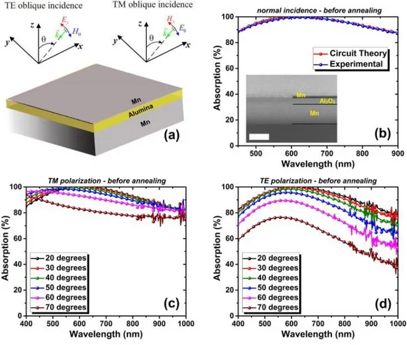
2.6 (a) Measured reflection, transmission and absorption spectrum of the fabricated MIM structure, inset: image of the fabricated sample, (b) comparison of simulation and calculation methods with measure-ment for the absorption spectrum of the optimal MIM structure, and, measured absorption of the MIM structure with different angles of incidence ranging from 20 to 70 degrees, for (c) TM and (d) TE po-larizations of incident light. Note that y-axis range is different be-tween (c) and (d) ... 22
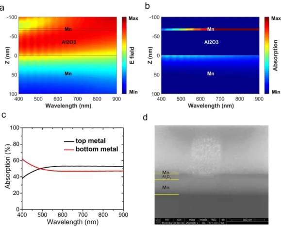
2.7 Simulated (a) electric field intensity and (b) absorption distribution in the cross section of the optimal MIM structure as a function of wavelength, (c) contribution of top and bottom metal layers in the light absorption and, (d) SEM image of the cross section of the fab-ricated MIM structure, milled by FIB ... 23
3.1 (a) Schematic of the MIM absorber, (b) Measured and circuit theory-based calculated absorption of the structure for normal incidence, inset: SEM image of the cross-section of the fabricated MIM ab-sorber, milled by FIB; the white scale bar represents 200 nm. The measured absorption spectra with different angles of incidence for (c) TM and (d) TE polarization. All of the figures correspond to the MIM sample before annealing ... 32
xv
3.2 (a) SEM images taken from the surface of the MIM sample, before and after annealing; the white scale bar represents 2 microns. (b) measured absorption of the sample before (red line) and after (blue line) annealing for the case of normal incidence, and, for different angles of incidence in the cases of (c) TM and (d) TE polarizations. Inset of (b) shows the image of the annealed fabricated sample ... 34
3.3 (a) Magnetic field magnitude, (b) electric field magnitude, and (c) absorption intensity distribution of on the xy cross-section of the center of the top metal layer of the annealed structure, simulated by importing the SEM image of the sample into the Lumerical FDTD solver ... 37
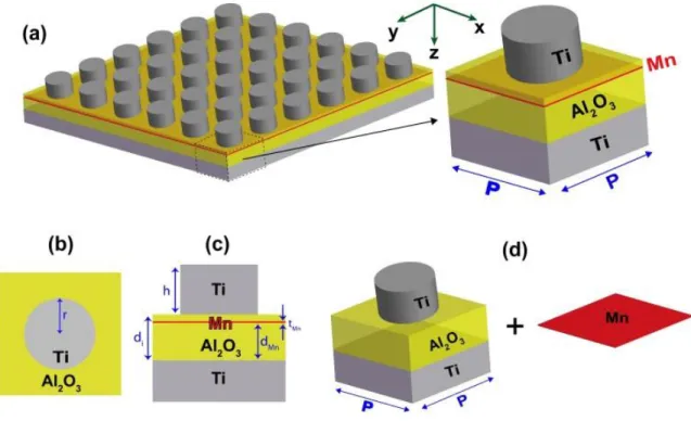
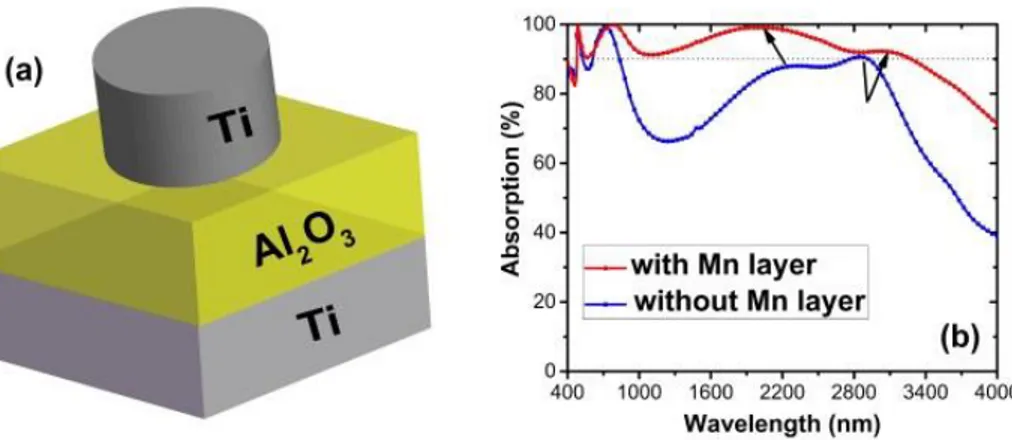
4.1 (a) Left plot: 3D schematic of the absorber; one unit cell of the struc-ture is bounded by dashed lines; right plot: a magnified view of one unit cell. (b) Top view, and (c) side view of the structure; and (d) the other image of the unit cell of the studied structure (perspective view): a patterned MIM configuration with top periodic layer com-posed of metal nanodisks, plus an ultra-thin Mn layer embedded into the insulator of the original configuration ... 42
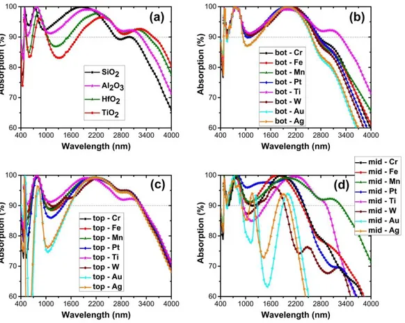
4.2 Absorption spectra for different materials of the (a) dielectric layer, (b) bottom metal layer, (c) top metallic nanodisks, and (d) middle ul-tra-thin metal layer, while using the same materials for the remain-ing components as in Fig. 4.1. The dimensions of the structure in all cases are: p = 480 nm, r = 140 nm, h = 180 nm, di = 165 nm, tMn = 5 nm, and dMn = 135 nm. The geometrical sizes in case of another material of the middle layer than Mn in (d) are the same as in case of Mn ... 44
4.3 Absorption spectra of the structure at different values of the radius of nanodisks (r), while period (p) is taken as (a) 440, (b) 460, (c) 480, (d) 500, (e) 520, and (f) 540 nm. In all figures, h = 180 nm and the materials are chosen in accordance to Fig. 4.1 ... 45
xvi
4.4 Absorption spectra of the structure at different values of the height of nanodisks (h), while period (p) is taken as (a) 440, (b) 460, (c) 480, (d) 500, (e) 520, and (f) 540 nm. In all figures, r = 140 nm and the materials are chosen in accordance to Fig. 4.1 ... 46
4.5 (a) Absorption spectra of the optimal structure calculated by FDTD (solid red line) and FIT (dashed black line) methods, along with contribution of each metallic layer to the absorption of the entire structure, and (b) absorption of the optimal structure (FDTD results) with magnified ordinate axis, to clearly demonstrate the peak posi-tions and bandwidth of the absorption ... 47
4.6 (a) 3D schematic of the unit cell of the structure without the Mn lay-er, and (b) absorption of the optimal structure with and without the Mn layer shown in red and blue colors, respectively ... 48
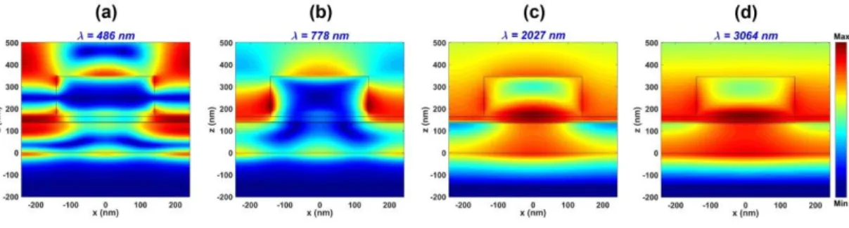
4.7 The spatial distribution pattern of the magnitude of the y-component of the magnetic field (Hy) in the xz cross-section of the structure at the (a) first, (b) second, (c) third, and (d) fourth absorption peak ... 50
4.8 (a) Absorption spectrum of the periodic array of Ti nanodisks on the Al2O3 substrate, with p = 480, h = 180, r = 140, di = 165 nm. (b) Absorption spectrum in case when bottom Ti layer is replaced by PEC, with the same dimensions as those of optimized structure. The insets show the schematics of the simulated structures ... 52
4.9 Absorption spectra of the optimal structure for different values of (a) p, (b) r, and (c) h; (d) Real (blue line) and imaginary (red line) parts of the normalized input impedance of the optimal structure, Zin, cal-culated using S-parameters, see Eq. (4.2) ... 55
4.10 (a) Real and (b) imaginary parts of the relative permittivity for Cr, Fe, Mn, Pt, Ti, W, Au, and Ag ... 56
xvii
4.11 Color plots of the absorption versus (a) p, (b) h, (c) r, (d) tMn, (e) di, and (f) dMn and the wavelength, for the purpose of demonstration of fabrication tolerance of the optimal structure. The dashed horizontal lines indicate the optimal value of the parameter under study ... 57
4.12 Absorption spectrum of the optimal structure for oblique incidence angles of 20, 40, and 60 degrees; (a) TM and (b) TE polarizations .... 58
5.1 a) Transmission, reflection, and absorption spectrum of a 600 nm thick planar Mn layer, b) Transmission, reflection, and absorption spectrum of a 600 nm thick suspended pyramidal array (shell) of Mn, and c) schematic of the random Si nano-pyramids before and after coating the surface with e-beam evaporated Mn shell like thin-film ... 63
5.2 SEM image from the surface of the Si wafer etched for a) 100, b) 200, c) 300, and d) 400 process cycles. e) Absorption spectra of the samples mentioned in (a), along with commercial Si wafer. Photo-graph of the Si wafers etched for f) 100, and g) 400 cycles ... 65
5.3 a) SEM image of the surface of the 300-cycle etched sample coated with 600 nm Mn, b) SEM image of the cross-section of the sample mentioned in (a) that is milled by FIB, c) AFM image of the surface topography of the sample mentioned in (a), and d) photograph of the sample mentioned in (a) ... 66
5.4 Absorption spectra of the fabricated samples with the three different Mn coating thicknesses of 400 nm, 600 nm, and 800 nm, for the cases of a) 200, b) 300, and c) 400 cycles of etching ... 68
5.5 a) 3D schematic of the approximated model along with its xz cross-section of its unit cell, b) Calculated reflection, transmission, and absorption spectrum of the structure when h=4, p=1, and t=0.6 mi-crons. Calculated absorption spectra for the incidence angles of 20
xviii
degrees, 40 degrees, and 60 degrees, for the case of c) TE polariza-tion, and d) TM polarization ... 69
5.6 Electric field magnitude distribution at the xz cross-section of the unit cell for different wavelengths of 2, 4, 6, 8, 10, 12 microns ... 71
5.7 a) Absorption spectrum of Si nano-pyramid array coated with Mn, Ti, W, Fe, and Cr, b) real part of relative permittivity, and c) absorp-tion spectrum of 600 nm thick planar film of the metals menabsorp-tioned in (a), d) Schematic of the light trapping nature of the structure, and, e) absorption spectrum of the nano-pyramid array of different sub-strates when coated with Mn ... 72
6.1 (a) 3D schematic of the MIM filter and, (b) the cross-section of the structure in (x,z)-plane. The names assigned to the thickness of lay-ers are demonstrated in (b) ... 78
6.2 Circuit model of the structure using the transmission line theory. The incident light approaches from the left side ... 79
6.3 The transmission spectrum (blue line) of the MIM structure with the metal layers chosen as Ag and the values of ni, dt, di, and db being 2.2, 25 nm, 70 nm, and 25 nm, respectively; the corresponding ver-tical axis being on the right side of the plot in blue color. The accu-mulated round-trip phase (red line) according to equation (6.1) cal-culated by using the proposed circuit model; the corresponding ver-tical axis being on the left side of the plot in red color ... 81
6.4 Contour plots of the magnitude of (a) the electric and, (b) the mag-netic field in different parts of the structure, the transmission spec-trum of which is shown in Fig. 6.3, versus the wavelength. The ver-tical dashed line crosses the wavelength of 550 nm, which corre-sponds to the resonance of this MIM filter ... 82
xix
6.5 The transmission spectrum of the MIM filter calculated for different values of di by using (a) the TMM, and, (c) the FDTD method, and for different values of ni by using (b) the TMM, and, (d) the FDTD method. Contour plots of the transmission spectra of the MIM filter (e) for varying values of di when ni is 2.2, and, (f) for varying values of ni when di is 70 nm, versus the wavelength, which are calculated by TMM, and, the output color as a function of wavelength is also shown below the plots in (e) and (f). In all cases, the material of both metal layers is chosen as Ag and the layers are 25 nm thick ... 84
6.6 The transmission spectrum of the MIM filter calculated (a) for all possible combinations of Ag and Au used in the metal layers, and for different pairs of (b) unequal and (c) equal values of dt and db when di is 70 nm and ni is 2.2, and both the metal layers are chosen as 25 nm thick Ag ... 85
6.7 (a) 3D schematic of the electrically tunable color filter ,(b) the trans-mission spectrum of the color filter for different values of the ap-plied voltage, (c) contour plots of the transmission spectra at contin-uous variation of applied voltage, the output color as a function of wavelength is also shown below the plot, (d) 3D surface plot of φtot versus wavelength and applied voltage; the meshed plane shows the zero-phase plane, and, (e) the resonance wavelengths versus the ap-plied voltage calculated from the phase condition (equation 6.1) and from the TMM method ... 88
6.8 The transmission spectrum of the electrically tunable color filter for different values of the applied voltage at the incidence angle of 45 degrees, for (a) TM and (b) TE polarization, calculated by the FDTD method, and for (c) TM and (d) TE polarization, calculated by the TMM method ... 89
7.1 a) 3D schematic of the structure, b) SEM image of the top view of the fabricated sample, and c) 2D cross-section of the of the structure
xx
along with the schematic of the incident, 0 order reflection, and -1 order diffraction beams ... 93
7.2 Simulated deflection efficiency of -1 order of the structure for TE polarization as a function of a) incidence angle and b) wavelength. Measured deflection efficiency contour plots of a) TE polarization -1 order, b) TE polarization 0 order, c) TM polarization --1 order, and d) TM polarization 0 order, as a function of wavelength and inci-dence angle. The white dashed lines in (c) represent iso-lines of con-stant -1 order reflection angles of -30, -40, and -50 degrees. The black dashed line in (c) represent the border where -1 order starts to appear ... 94
7.3 Measured deflection efficiency contour plots of -1 reflection order of the structure for a) TE and b) TM polarizations, as a function of wavelength and incidence angle ... 96
7.4 Spatial filter functionalities of the structure. Deflection efficiency of a) TE polarization at 0 order at the wavelengths of 890, 900, and 910 nm, b) TE polarization at 0 order at the wavelengths of 1500, 1700, 1900, and 2100 nm, c) TE polarization at -2 order at the wave-lengths of 770,780, and 790 nm, and d) TM polarization at -3 order at the wavelengths of 550, 560, and 570 nm ... 98
7.5 Beam splitter functionality of the structure. Deflection efficiency of TE polarization at a) -1 order, b) -2 order, and c) sum of -1 and -2 orders, at the wavelengths of 1030, 1050, and 1070 nm ... 99
1
Chapter 1
Introduction
1.1 Background
This chapter is on part reprinted with permission from: 1. Majid Aalizadeh, A. Khavasi, B. Butun, and E. Ozbay, “Large-Area, Cost-Effective, Ultra-Broadband Per-fect Absorber Utilizing Manganese in Metal-Insulator-Metal Structure,” Scientific
Reports, vol. 8, p. 9162, 2018, and 2. Majid Aalizadeh, A. E. Serebryannikov, A.
Khavasi, G. A. E. Vandenbosch, and E. Ozbay, “Toward Electrically Tunable, Lithography-Free, Ultra-Thin Color Filters Covering the Whole Visible Spectrum,”
Scientific Reports, vol. 8, p. 11316, 2018.
Natural materials have limitations in their optical performance. They either have to be too bulky to be used for optical applications, or do not perform as efficient as re-quired. Metamaterials, consisting of natural materials but in specific designs, have made it possible to come up with subwavelength structures that can function much more efficient compared to the natural materials.
In this thesis, three important applications of metamaterials are explored: 1. Ultra-broadband and lithography-free absorbers, 2. Lithography-free electrically tunable color filters, and 3. Wideband and wide-angle beam deflector and multifunctional an-gular filter metasurfaces.
2
1.1.1
Broadband Absorbers
Electromagnetic (EM) wave absorbers have attracted a lot of interest in technolo-gy, because of their vast range of applications in photovoltaics [1-4], shielding [5, 6], thermal imaging [7-9], sensing [10-12], photodetection [13-17], and thermal emis-sion-based cooling [18, 19]. With the advent of plasmonics [20] and metamaterials, it became possible to design absorbers with ultra-thin sub-wavelength thicknesses, which is of high importance for optical packed circuit integration and the reduction of mass and cost of structures.
The general requirements for an absorber structure to absorb electro-magnetic (EM) energy are having impedance matching with free space to minimize reflection [21, 22] as well as near to zero transmission. One of methods to absorb light is to trap EM wave in a resonance mode of light and to absorb it by means of loss mechanisms such as electron collisions. The common resonance modes used in the design of ab-sorbers are Localized Surface Plasmon (LSP) modes [23-27], Propagating Surface Plasmon (PSP) modes [28, 29] and Fabry-Perot resonance modes [30, 31]. To obtain broadband absorption, we can broaden the resonance bandwidth by sufficiently low-ering the quality-factor with the appropriate choice of metals and the geometric de-sign. The other approach is to design the structure in a way to have the superposition of several adjacent resonance modes and, therefore, broaden the absorption spectrum.
It is of high importance for the broadband absorber to be designed in a way to have large-scale production compatibility. One big barrier to large-scale production is the use of lithography in the structures, which is time consuming and costly. In order to have mass production compatibility, it is also very beneficial to use inexpensive ma-terials in the structure. Therefore, designing a broadband lithography-free absorber in which inexpensive materials are used is very advantageous and meets the require-ments of large-scale production.
In one of the pioneer works that was based on the superposition of LSPs, Aydin et al. [32] achieved an average of 71 percent absorption in the visible region (400-700 nm), by superposing the LSP modes of varying width of nanorods. However, it was achieved by use of Electron Beam Lithography (EBL). Some other works are
fabri-3
cated or designed to obtain broadband absorption in the visible [33-35], near-infrared (NIR) [36, 37], mid-infrared (MIR) [38-41], far-Infrared (FIR) [42], and Terahertz [43-46] ranges by using EBL and implementing the above-mentioned ideas.
In a recent lithography-free work conducted in our group, 97 percent absorption was achieved from 400 to 2000 nm wavelength by employing the superposition of LSP modes of dielectric-metal core-shell nanowires. This broadband perfect absorp-tion was the result of randomness in the size of chemically synthesized nanowires [47]. One other common method to broaden the absorption band without the use of lithography is to anneal the structure in high temperatures, which is called the De-wetting process [48]. This leads thin layers to reform into nanoholes or nanoparticles, and adds the superposition of the LSP modes of nanopatterns into the absorption bandwidth. Some works are done in our group to broaden the absorption of Metal-Insulator-Metal-Insulator (MIMI) structure using this method [49, 50]. However, this comes with the cost of access to very high temperatures, which is time consuming and always brings the possibility of sample cracking, especially for the ones with thin substrates.
As mentioned earlier, lowering the quality factor of Fabry-Perot resonance is an-other way to achieve broadband absorption without lithography. This resonance can be obtained by making a Fabry-Perot resonator using an MIM structure. By adding the number of Metal-Insulator (MI) pairs, a broader bandwidth can be obtained. Some lithography-free works have achieved broadband absorption by employing MI multi-layer stacks. These works are done by using different combinations of MI pairs such as Cr-SiO2 [51], W-Al2O3 [52], Ti-SiO2 [53], and W-Al2O3-Ti- Al2O3 [54]. Also in a
re-cent lithography-free work, broadband infrared absorption is obtained by implement-ing ITO-photoresist pairs [55].
1.1.2
Tunable Color Filters
The electromagnetic (EM) response of an optical device depends on the dimensions and material parameters of its components. This often imposes a limitation on their tuning functionality in a way that the EM response gets determined at the stage of
4
fabrication, since new dimensions and/or materials are required to obtain a new EM response. To obtain the possibility of real-time tuning of the EM response of optical structures after the fabrication, dynamically tunable ideas are required to be imple-mented. Among different ways of tuning, tuning with variable voltage (electrical tun-ing) has always been the most desirable and has been the topic of extensive research over the last decade. For this purpose, different methods and materials have been suggested. Utilizing electro-optically active materials is one of the most common methods for electrical tuning of optical structures. Optical behavior of these materials is modified by applying voltage. Liquid crystals [56-59], organic crystals [60-62], graphene [63-66], heavily doped compounds like Al-doped ZnO (AZO) [67] or n-type Indium Antimonide (n-InSb) [68], and transparent conductive oxides like Indium Tin Oxide (ITO) [69-74] or Indium Zinc Oxide (IZO) [75] are common materials used for this purpose. The choice of an electro-optic (EO) material depends on the design and the operating wavelength range of the optical structure. It is noteworthy that micro-electro-mechanical systems (MEMS) or nano-electro-mechanical systems (NEMS) have also been used to provide optical devices with the possibility of real-time controlling [76, 77].
Recently, several works have been reported, in which ITO is used to electrically tune the reflection spectrum of the optical structures, in particular, the one of the re-flect-array metasurfaces [69-74]. Some works have been dedicated to the use of ITO as the tunable material to actively steer the reflected beam of metasurfaces [73, 74]. The structures involving ITO as the active material generally use it in the configura-tion of Metal-Oxide-Semiconductor (MOS) capacitor, so that by applying voltage, the carrier concentration of ITO changes in the vicinity of the ITO-oxide interface. These changes lead to those in the plasma frequency of the Drude model of the permittivity of ITO, and thus modulate the permittivity and the refractive index profile of ITO [78]. This is how the optical response of such structures gets tuned by the application of voltage.
A number of works have also used graphene as the active material [63-66]. The tuning in these works has been possible due to the shift in the Fermi energy level of graphene, which is obtainable by applying a bias voltage, so that the optical response of graphene and the whole structure is changed.
5
Color generators represent a wide class of the optical devices having various ap-plications including displays, printing technologies, imaging, and light emitters. Some structural color generators are available in nature in specific types of insects, birds, and animals, such as butterfly wings [79-83].Initial artificial color displays have em-ployed liquid crystals, and produce the three main colors, red, green, and blue [84-86]. Recently, metamaterials have been introduced as a new platform that enables the realization of color displays with higher compactness, better resolution, better power-efficiency, and more flexibility in design-based color tunability. There are a lot of works demonstrating color filters without the possibility of real-time tuning [31, 87-93]. At the same time, tunable color filters working in the transmission or reflection mode have also been reported; some of which are dynamically controllable by the polarization of incident light [94-96], while some others are electrically tunable [56, 59, 68, 97]. For example, it has been suggested to use a polarization-tailored dichroic resonator combined with a twisted nematic liquid crystal [98]. However, in this case, lithography is required in the fabrication process.
In most of the earlier works, lithography is typically required as a part of fabrica-tion process, which is the main barrier to mass producfabrica-tion. It brings many limitafabrica-tions such as significantly restricting the area of samples, decreasing the throughput, and increasing the cost of fabrication. Therefore, coming up with a lithography-free de-sign is of great importance for the purpose of large-area production and cost reduc-tion. A lithography-free approach has been recently proposed in a few works for color filters, which cannot be tuned in real time [73, 74]. These series of lithography-free bandpass filters are based on the MIM cavities and work in the transmission mode.
1.1.3
Beam Deflectors and Angular Filters
Electromagnetic beam manipulation has attracted a lot of interest in recent decades. Beam deflection and anomalous reflection is one important type of beam manipula-tion applicamanipula-tion for wave-front engineering devices. The previous structures used for beam deflection include photonic crystals, hyperbolic metamaterials, gratings [99, 100], phased arrays, and metasurfaces [101, 102]. However, most of them either have a limited efficiency or do not have wideband and wide-angle desired behavior.
6
Another highly-demanded type of beam manipulation is the filtering functionality. Filtering can be realized both in the frequency and incidence angle domain, which are called spectral and spatial filtering, respectively. Spatial filtering is the possibility of passing or rejecting beams with a specific direction of incidence into another speci-fied direction. These direction selective spatial filters (SFs) along with the spectral filters are of high importance in optics and have applications in detection, sensing, and imaging.
Some spatial filters were reported previously which were based on photonic crys-tals [103-105], resonant and non-resonant grating structures [106, 107], axisymmetric photonic microstructures [108], hyperbolic metamaterials [109], and waveguide-based systems [110]. Nevertheless, they are typically designed to have single func-tionality and often perform as one type of SF, i.e. either function as pass, band-stop, low-pass, or high-pass filters.
1.2 Thesis Outline
Chapters 2 to 5 are dedicated to four different broadband absorbers with the inclusion of Mn. Mn is introduced as a promising metal for broadband absorbers for the first time and it is shown in all works that it demonstrates a superior performance com-pared to other metals. In chapter 2, Mn is used in the basic MIM configuration and by using this lithography-free structure, above 94% average absorption is obtained in the wavelength range of 400-900 nm. Chapter 3 shows how annealing the Mn-based MIM structure boosts the broadband absorption performance. It is shown that by an-nealing the structure, random nanoholes appear in the top thin Mn layer that can sup-port Localized Surface Plasmon modes, the superposition of which leads to broaden-ing the absorption spectrum of the MIM cavity with a 2.1-fold enhancement. An av-erage absorption of above 94% is achieved in the range of 450-1400 nm, using this lithography-free structure. In another attempt in chapter 4, it is shown that embedding an ultra-thin Mn layer inside the top-layer-patterned MIM cavity enhances the ab-sorption band at about tenfold. As the last work on broadband absorbers, UV to FIR
7
absorption is achieved by coating a single layer of Mn on any high-roughness sub-strate and the results are presented in chapter 5.
In chapter 6, by exploiting an electro-optic dielectric in the insulator section of the MIM filter, we have achieved a lithography-free color filter that covers the whole vis-ible spectrum by applying -12 to 12 volts of voltage.
Chapter 7 shows that by using a simple structure consisting of Silicon nanorods, highly-efficient, wideband and wide-angle beam deflection is achievable. This metasurface also shows multiple angular filtering functionalities as pass, band-stop, and low-pass spatial filters.
8
Chapter 2
Manganese-Based MIM Cavity
This chapter is on part reprinted with permission from: Majid Aalizadeh, A. Khava-si, B. Butun, and E. Ozbay, “Large-Area, Cost-Effective, Ultra-Broadband Perfect Absorber Utilizing Manganese in Metal-Insulator-Metal Structure,” Scientific
Re-ports, vol. 8, p. 9162, 2018.
2.1 Introduction
It is known well that the MI-stack broadband absorbers have at least four layers (two MI pairs) in their structure. However, the purpose of this section is not to design an MI-stack absorber. We want to design a broadband absorber using the tri-layer MIM structure, which is the simplest possible configuration for absorbers. Moreover, as mentioned before, the MI-stack absorbers are discussed in several works, but, to the best of our knowledge, there are very few tri-layer broadband, lithography-free and annealing-free absorbers, reported previously [111].
In the present section, we experimentally demonstrate lithography-free, ultra-broadband nearly perfect absorption within 400-900 nm range by the MIM structure. The measured average absorption in this wavelength range is above 94 percent by the use of Mn in the metal layers. The most important difference between our work in this section and earlier works is that we introduce Mn for the first time in broadband
9
absorbers, and, by detailed analysis, we show that it is a very promising metal for achieving maximum absorption in broadband absorption applications. It is also an inexpensive metal unlike gold or silver, which can reduce the cost of fabrication in favor of mass production. Also, the proposed structure does not need post-annealing.
In the following parts of this section, first, MIM cavities and formulation of their resonance modes is discussed. Then, the optimization process of this structure is ex-plained in detail in terms of two factors: 1. Materials and 2. Dimensions. First, to op-timize the structure by choosing the appropriate materials, the effect of dielectric ma-terial is investigated, and also it has been demonstrated numerically that the best choice of metal is Mn for this structure. During the optimizations and calculations, the structure is modeled by using the Transfer Matrix Method (TMM) and also circuit theory. Some of simulations are also performed by the Finite Difference Time Do-main (FDTD) method. It is also conceptually demonstrated as to how Mn is such an appropriate metal for the MIM structure and for broadband absorbers in general, by discussing based on its permittivity profile. Then, the structure is optimized in terms of the dimensions of different layers. At the end, the optimal structure has been fabri-cated and characterized. The experimental results are in good agreement with simula-tions and calculasimula-tions showing a very large absorption bandwidth.
2.2 Design and Theory
Figure 2.1(a) depicts a 3D graphical schematic of the MIM structure and Fig. 2.1(b) shows its 2D cross section in xz plane. The bottom layer is an optically thick metal layer that is much thicker than the skin depth of the metal to ensure zero transmission. The middle insulator layer can be chosen among different dielectrics, taking into ac-count the fact that the refractive index of the dielectric is an important parameter in determining the resonance frequency of the cavity mode. The top layer must be opti-cally thin to allow the coupling of the incident light into the MIM cavity and conse-quently getting trapped inside it with back and forth reflections from metals. The trapped light is partly absorbed in each reflection, eventually, leading to complete ab-sorption.
10
The resonance mode of the asymmetric Fabry-Perot cavity shaped by this MIM structure follows the equation of the form [30]:
2 2 i i b t 2 res n d m (2.1)
where λres is the resonance wavelength, ni and di are the refractive index and thickness
of the insulator layer, respectively, and m is an integer number which determines the order of cavity mode. It can be deduced from equation (2.1) that higher order cavity modes resonate at smaller wavelengths. φb and φt are the phase shift acquired from
reflection from the bottom and top metal layers, respectively. It is noteworthy that equation (2.1) along with all other analytical theories presented throughout this sec-tion is only applicable for normal incidence. It can be seen that by increasing ni or di,
λres increases as well. In other words, by increasing the optical beam path which is
written as nidi, the resonance wavelength red-shifts. Therefore, to modify the center of
the absorption band, one can use dielectrics with different refractive indices or adjust its thickness according to the absorption band of desire. To achieve broadband ab-sorption, the quality-factor of cavity mode should be sufficiently low, which is essen-tially obtained by the correct choice of metal.
To calculate absorption (A), reflection (R) and transmission (T) must be calculated and then absorption can be obtained from the A=1-R-T formula. In the present sec-tion, TMM is used for these calculations, and the results are verified by FDTD simu-lations and circuit theory calcusimu-lations. It should be noted that, for a sufficiently thick bottom metal layer, T is almost zero and, therefore, the absorption is simplified to A=1-R. To be more precise, however, we include T in our calculations.
2.2.1
Material Optimizations
In this part, the effect of dielectric material and the metal is investigated and the op-timized materials are chosen among them.
11
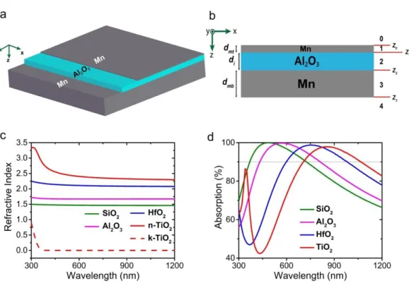
Figure 2.1: (a) 3D schematic of the proposed MIM structure, (b) cross section of the structure in xz plane, (c) refractive index of four common dielectrics investigated in the absorption calculations and, (d) calculated absorption spectrum of MIM structure.
Fig. 2.1 (c) shows the refractive index of four different common dielectrics: SiO2,
Al2O3, HfO2 and TiO2, and Fig. 2.1 (d) shows the calculated absorption spectrum of
MIM using the four mentioned dielectrics, while keeping the metal (Mn) and all di-mensions constant. The thickness of the layers from bottom to top is 200, 65, and 5 nm, respectively. As expected, the absorption mode red-shifts as the refractive index of the dielectric material increases. Since we have the possibility to deposit Al2O3 by
Atomic Layer Deposition (ALD) which deposits layers with lower roughness, the die-lectric material is chosen to be Al2O3 for the rest of this work. It has to be mentioned
that based on previous explanations and as it will be demonstrated in detail in the fol-lowing sections, this thickness of the insulator layer, 65 nm, has been chosen by using Al2O3 to obtain high absorption in the desired bandwidth of 400-900 nm. It should be
noted that other dielectrics can also be used, considering the fact that in order to achieve high absorption in the same wavelength band, the thickness of the dielectric layer should be calculated accordingly and the optimized thickness for this layer will be different from 65 nm.
12
In order to choose the most appropriate metal, as it will be elevated in detail in the next parts, the input impedance of the structure should be calculated. Therefore, first the calculation of the input impedance is explained. The input impedance of the pro-posed three-layer structure is calculated by circuit theory.
The equivalent circuit of the structure is shown in Fig. 2.2 (a). At normal inci-dence, βm and Zm are the propagation constant and characteristic impedance
(normal-ized to the impedance of free space) of the transmission line corresponding to the metal layer and are equal to nmβ0 and 1/nm, respectively, with nm denoting the
refrac-tive index of the metal and β0 denoting the propagation constant of light in vacuum. βi
and Zi are similarly the corresponding parameters for the transmission line modeling
the insulator layer. Finally, Z0 is the normalized impedance of free space, which is
equal to 1. It is assumed in this model that both the top and bottom metal layers have the same material, therefore, for both layers, the characteristic parameters are denoted with the subscript of ‘m’.
To better understand the mechanism of the absorption, we simplify the equivalent circuit by modeling the top thin metal layer with a surface conductivity, which is an accurate approximation for ultra-thin layers [39]. The characteristic equivalent admit-tance (surface conductivity) of the top layer (normalized to free space admitadmit-tance) is
(1
)
mt m mt
Y
j
d
c
(2.2)where c is the free space speed of light and ω is the angular frequency. ɛm denotes the
relative permittivity of metal, and dmt represents the top metal layer thickness. The
above equation is obtained by approximating the bulk conductivity by surface con-ductivity when the layer is ultra-thin. Then the value of equivalent admittance of that layer is equal to the value of surface conductivity.
The second approximation is assuming the bottom metal layer thickness to be infi-nite. Therefore, Z1 in Fig. 2.2(a) can be replaced by a load impedance of Zm. Thus, the
13
The input impedance seen from the interface of the top metal and the dielectric layer which is denoted as Z2 in figures 2.2(a) and 2.2(b) can be written as [112]
2 tan tan m i i i i i m i i Z jZ d Z Z Z jZ d
(2.3)In this approach, the admittance of top Mn layer or Ymt is parallel to the equivalent
input admittance of the other two layers which is equal to the inverse of input imped-ance of these two layers or Z2. The total input admittance then, is the sum of
admit-tances Ymt and Y2.
After calculating the input impedance (admittance) of the structure, the reflection of the structure, can be calculated by the following formula
2 1 R 1 in in Z Z (2.4)
which is the well-known relation for reflection at the interface of two media with dif-ferent impedances. Now, we approximate T to be zero, which is a very good approx-imation for a sufficiently thick bottom layer. We show the accuracy of this approxi-mation by calculating transmission in the next sections. Therefore, the absorption can be simply calculated as A=1-R.
Now, for choosing the appropriate metal, we assume that the top and bottom metal layers both are chosen as the same material. Then we try to find the best metal for the structure. The material of metal layers plays the main role in determining the quality factor of the cavity. For this purpose, we calculate the normalized input impedance of the structure using circuit theory and then we equate it to the impedance of free space (i.e. 1). This is the condition for having zero reflection. From there the permittivity of the ideal metal can be calculated. Thereafter, the metal with the closest permittivity profile to the ideal metal should be chosen. During this calculation, the dimensions are 5, 65, and 200 nm, respectively and Al2O3 has been used as the insulator layer.
14
Figure 2.2: (a) Equivalent circuit of the MIM structure, (b) simplified equivalent cir-cuit model of the MIM structure, (c) real and (d) imaginary part of permittivity of Mn and the ideal metal, along with those of Ti, W, Cr, Pt, and Au that are commonly reported metals for broadband absorption, (e) calculated absorption spectrum of the MIM structure using metals mentioned in (c) and (d). (f) Real and imaginary part of input impedance of the structure using Mn (black solid and dashed lines), normalized to free-space impedance, and reflection calculatedusing circuit theory (red line).
15
The calculated real and imaginary parts of relative permittivity profile of the ideal metal as well as some other metals are shown in Fig. 2.2 (c) and Fig. 2.2 (d), respec-tively. The metals are Titanium (Ti), Tungsten (W), Platinum (Pt), Chromium (Cr), and Gold (Au). Apart from Au, other metals are the candidates reported so far for broadband absorption applications, especially for lithography-free structures. Au can be used for broadband absorption in the case of patterning. The permittivities of the above-mentioned metals are plotted in these figures along with Mn, for a fine com-parison between their permittivity profile and the one for ideal metal. The permittivity of the ideal metal is shown by black dashed lines in figures 2.2 (c) and (d). As it is obvious from both figures 2.2 (c) and 2.2(d), Mn has the closest permittivity profile to the ideal metal. It can be observed that the imaginary part of permittivity of the ideal metal is very close to that of Mn, from 400 nm up to around 600 nm. On the other hand, after 600 nm, up to the end of our desired spectrum, i.e., 900 nm, the real part of permittivity of Mn is similar to the real part of permittivity of the ideal metal. This demonstrates that Mn is the best candidate for our structure in our bandwidth of inter-est. So we choose Mn for the rest of our work as the top and bottom layer metal. It can be observed that around the calculated absorption peak wavelength, both the real and imaginary parts of permittivity of Mn almost intersect with the one for ideal met-al. The material data of Mn and Al2O3 shown here, and also used in all the
simula-tions and calculasimula-tions, have been obtained by fitting spectroscopic data obtained from ellipsometry measurements. Material data for all other metals except for Au are ob-tained from Palik and for Au the data are obob-tained from Johnson and Christy.
Figure 2.2 (e) shows calculated absorption when the 5 different mentioned metals are used, along with the case of using Mn. It is obviously notable that, as predicted, Mn has the best absorption in terms of absorption strength and bandwidth at the same time. This is due to the fact that using Mn provides a better and broader impedance matching to free-space that leads to the minimization of reflection and trapping of light in a broad spectrum. Figure 2.2 (f) shows the real and imaginary parts of the cal-culated input impedance of the structure normalized to that of free-space, as well as reflection calculated using equation (2.4). It can be seen from this figure that the rea-son of having a broad dip in the reflection spectrum (broad absorption peak) of this structure lies in the fact that the real part of input impedance is close to 1 in a broad
16
wavelength band, while the imaginary part of it is close to zero. This minimizes the reflection and provides a broadband impedance matching to the free space.
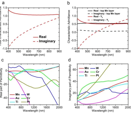
Figure 2.3 (a) shows the input admittance of the structure. To have admittance matching with free space, similar to impedance matching, the real part of input admit-tance must be close to 1 and its imaginary part must be close to zero, which is the case here as it can be seen from Fig. 2.3 (a). The admittance matching process reveals better why Mn is such an appropriate metal for this structure. The real and imaginary parts of the equivalent admittance of top Mn layer and the input admittance seen from the dielectric and the top metal interface which is denoted as Y2 in Fig. 2.2 (b), are
shown in Fig. 2.3 (b). It is obvious that the real part of Y2 is around 0.5 within the
wavelength range of interest. The other required 0.5 of admittance for admittance matching is provided with the admittance of top Mn layer, as it can be seen in the fig-ure. Fig. 2.3 (a) shows that the real part of input admittance of the structure stays around 1, but its imaginary part does not have such a behavior and its absolute value grows by getting far from the resonance wavelength. This limits near-to-perfect ab-sorption to around 400-900 nm. It can be seen from Fig. 2.3 (b) that the imaginary part of admittance of the top Mn layer is around zero and, therefore, has almost no contribution to admittance mismatch happening outside the bandwidth.
Figures 2.3 (c) and (d) show the real and imaginary part of relative permittivity of Mn along with previously mentioned other 5 metals in a broad wavelength range be-tween 400 and 2000 nm. By taking a look at these figures one can understand more about the physical reason behind broadband absorptive behavior of Mn. Compared to other metals, Mn has a very slowly changing real part of permittivity in the broad range of 400-2000 nm, covering visible and NIR, which makes impedance matching of the structure to that of free space easy. Its real part of permittivity has small values in this broad spectrum, which leads to high field penetration; and, at the same time it has a large imaginary part of permittivity that leads to high absorption. The lossy be-havior of Mn results in a low quality factor Fabry-Perot MIM cavity. On the other hand, some other metals such as Gold and Silver have a very narrowband MIM cavity mode, because they are low loss metals.
17
Figure 2.3: (a) Total characteristic admittance of the structure, calculated by circuit theory, (b) characteristic admittance of top Mn layer modelled as surface conductivity and characteristic input admittance of other two layers looking from top of Al2O3
(denoted as Y2 in Fig. 2.2 (b)), (c) real and (d) imaginary part of permittivity of Mn
along with those of the other 5 metals, extended up to 2000 nm wavelength.
So far, we have thoroughly investigated the effect of materials and highlighted the importance of the choice of metals. The above discussions show what a great poten-tial Mn has to be employed in broadband absorption structures, even in higher wave-length ranges. Unlike its high potential, it has not been employed in absorbers so far. Therefore, we choose Mn for metal layers and Al2O3 as the dielectric layer for the
18
2.2.2
Dimension Optimization
As explained in the previous parts of this section, by increasing the thickness of the insulator layer, the optical path of the light inside the structure increases and the ab-sorption band experiences a red-shift (see equation 2.1). One way to tailor the optical beam path (nidi) is changing the dielectric material that indeed changes ni in equation
2.1 that was explained in the previous section. The other method is the control of di.
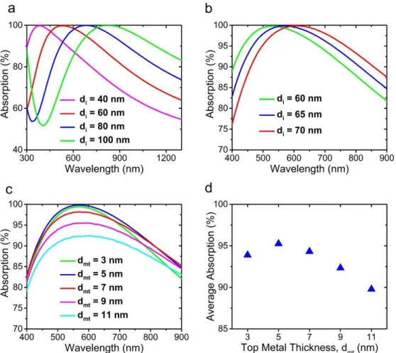
Figure 2.4: Calculated absorption spectrum of MIM structure for the different values of di with (a) 20 nm steps and, (b) 5 nm steps, while Mn is assumed as the metal and
the top layer thickness is dmt = 5 nm, (c) calculated absorption spectrum of MIM
structure for different values of dmt and, (d) average absorption for different values of
dmt calculated in the 400–900 nm wavelength range, again Mn is assumed as the
metal and the thickness of the dielectric layer is di = 65 nm.
Fig. 2.4 (a) demonstrates the effect of the thickness of the insulator layer on the ab-sorption spectrum. It can be observed that by choosing thicker dielectrics, the absorp-tion band red-shifts. Among the calculated absorpabsorp-tions for different dielectric
thick-19
nesses, the one for 60 nm matches our desired spectrum, i.e. the visible range and some parts of NIR. For finely tuning the dielectric thickness, absorption spectrum has been calculated for different di values of 60, 65, and 70 nm as shown in Fig. 2.4 (b).
As it can be seen from Fig. 2.4 (b), in the case of choosing 60 nm, the absorption strength will decrease in NIR range and, on the other hand, by choosing 70 nm as the dielectric thickness, absorption strength decreases in shorter wavelengths of visible range; but in the case of 65 nm, the best overall absorption strength and almost per-fect absorption is obtained within the broad range of 400 nm to 900 nm wavelength. Therefore, di is chosen to be 65 nm.
Now, to choose the best thickness for the top metal layer or dmt, absorption for
dif-ferent values of dmt ranging from 3 to 11 nm has been calculated and is shown in Fig.
2.4 (c). It is obvious that the 5 nm is the best thickness for the top layer because it has the strongest and broadest response compared to the other dmt values. Fig. 2.4 (d)
il-lustrates the average absorption calculated in the 400 to 900 nm wavelength range versus dmt, again demonstrating that 5 nm is the best choice for the top layer
thick-ness.
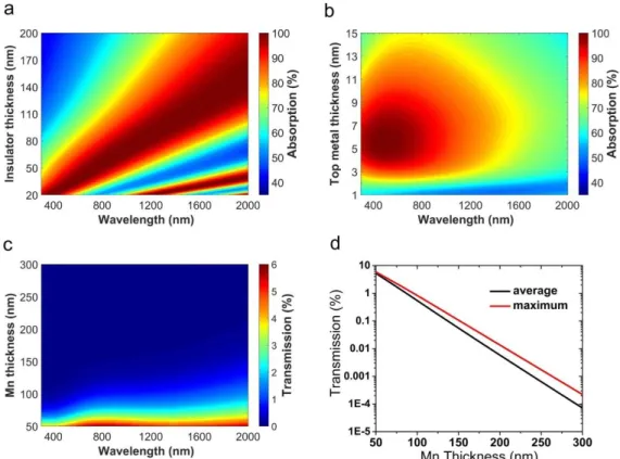
To investigate the fabrication tolerance of the structure, which is a very important factor for mass production purposes, we have calculated the absorption of the struc-ture for varying di versus wavelength and also for varying dmt versus wavelength as
shown in Fig. 2.5 (a) and (b), respectively. These color-plots show that deviations from optimal dimensions in the order of a few nanometers do not affect the absorp-tion bandwidth and strength, significantly.
As for the bottom layer, there is no optimization needed and it is only necessary to be thick enough so that it almost completely blocks the transmission.
Fig. 2.5 (c) depicts the transmission for different thicknesses and varying wave-length and gives a good insight about this issue. There is a slight increase in transmis-sion toward higher wavelengths that is due to the decrease of the optical path inside the material which leads to reduction of absorption of the light passing through it. Fig. 2.5 (d) shows the maximum and average transmission in the range of 400-900 nm versus Mn thickness. It is obvious that maximum transmission remains below 1
per-20
cent for thicknesses down to around 100 nm. Based on these figures, we conserva-tively set the thickness of the bottom Mn layer to 200 nm.
Figure 2.5: (a) Calculated absorption of MIM structure versus the wavelength and different values of di, assuming Mn as the metal with dmt = 5 nm and Al2O3 as the
dielectric, (b) same as (a) but for different values of dmt and with di = 65 nm, (c)
calculated transmission from a layer of Mn versus wavelength and different thicknesses of Mn layer and, (d) maximum and average values of transmission from a layer of Mn versus Mn thickness, calculated in the 400-900 nm wavelength range.
To summarize, the optimized structure is as follows: The dielectric is chosen to be Al2O3 and the metal is Mn. The dimensions of 5, 65 and 200 nm are chosen for the
top metallic layer, dielectric insulator, and the bottom thick metal layer, respectively. In the next section, we present the experimental results for this structure.
21
2.3 Results and Discussion
The structure with optimized dimensions was fabricated and characterized. In order to avoid any contribution from the substrate to the absorption, and also to be able to measure the transmission of MIM, the structure has been fabricated on a transparent Sapphire substrate. Fig. 2.6 (a) shows the measured transmission, reflection and ab-sorption of the structure for the case of normal incidence. The experimental result for absorption demonstrates over 94 percent average absorption in the broad range of 400-900 nm and has absorption as high as 99.6 percent at the wavelength of 626.4 nm. The image of the fabricated absorber is shown in the inset of Fig. 2.6 (a) which demonstrates the black color of the absorber due to the strong absorption of the visi-ble light. Moreover, as expected, the measurements confirm that the structure has ze-ro transmission.
The experimental results are compared against simulation results calculated with the circuit model, TMM and FDTD, in Fig. 2.6 (b). It is obvious that the simulation and experimental results are in good agreement. The insignificant mismatch between the simulation and experimental results may be due to using different deposition rates for the top and bottom metal layers (see Methods, Experimental). The permittivity profile of Mn has been extracted from a film deposited by the same rate as the bottom metal. Therefore, since using different deposition rates may affect the grain size which may consequently affect the optical properties, the optical properties of the top metal layer may be slightly different. However, this possible difference in the optical properties must have been insignificant because of the negligible mismatch between theory and experiment. Other possible causes may be variations in the thickness of the layers and also imperfections in the roughness of the top layer since it is very thin and it is hard to obtain ultra-thin metallic layers with no roughness while using physi-cal vapor deposition methods. However, for broadband absorbers, roughness is a positive characteristic and contributes to the strength and also the broadening of the absorption because it leads to having the superposition of various modes in the ab-sorption.
22
Now let us investigate the performance of the fabricated structure for oblique inci-dence and to show that it has an omnidirectional performance, which is very im-portant in different applications. We measured the absorption of the structure for both TM and TE polarizations and for angles ranging from 20 to 70 degrees. Figures 2.6 (c) and 2.6 (d) show the absorption of the structure for the mentioned incident angles in the wavelength range of 400 to 900 nm, for TM and TE polarizations, respectively. It is obvious that the device retains its high and broadband absorption performance up to very large incident angles such as 70 degrees for TM polarization. However, the TE polarization is more sensitive to the variations of incident angle. Note that the range of y-axis is different for figures 2.6 (c) and 2.6 (d).
Figure 2.6: (a) Measured reflection, transmission and absorption spectrum of the fabricated MIM structure, inset: image of the fabricated sample, (b) comparison of simulation and calculation methods with measurement for the absorption spectrum of the optimal MIM structure, and, measured absorption of the MIM structure with different angles of incidence ranging from 20 to 70 degrees, for (c) TM and (d) TE polarizations of incident light. Note that y-axis range is different between (c) and (d).
23
To further elucidate the electromagnetic phenomena taking place in this structure, the electric field distribution inside the structure for the wavelength range of interest (400-900 nm) is depicted in Fig. 2.7 (a). Since the structure is not changing in the lat-eral direction, we have only depicted the vertical spatial variation of the field inside the structure. It is obvious that a cavity resonance mode is trapped inside the structure in the dielectric region and back and forth reflections from the top and bottom metal-lic layers lead to a standing wave inside it.
Figure 2.7: Simulated (a) electric field intensity and (b) absorption distribution in the cross section of the optimal MIM structure as a function of wavelength, (c) contribution of top and bottom metal layers in the light absorption and, (d) SEM image of the cross section of the fabricated MIM structure, milled by FIB
To better observe the contribution of each layer to absorption, the absorption in-tensity in different layers in the structure versus wavelength is shown in fig. 2.7 (b). It can be seen that the absorption intensity is high at the top metal, but it is accumulated in a thin layer. In the bottom metal, on the other hand, the absorption intensity is
low-24
er compared to the top metal, but it is distributed in a thicker layer. To evaluate the total contribution of each layer to absorption, Fig. 2.7 (c) shows the percentage of to-tal absorption in each meto-tallic layer, versus wavelength. It can be observed that the contribution of the top and bottom metallic layers is not significantly different. As can be seen in both figures 2.7 (b) and (c), at lower wavelengths, the bottom layer has a larger contribution to the absorption and the absorption of the top metal layer increas-es at longer wavelengths. Finally, the Scanning Electron Microscopy (SEM) image of the cross section of the fabricated sample, which is milled by Focused Ion Beam (FIB) is shown in Fig. 2.7 (d).
2.4 Conclusion
Step-by-step design and optimization of a broadband MIM absorber is presented, ge-ometrically and in terms of materials. The important advantage of this absorber is the use of three large area layers without any need to lithography or any repetition of MI pairs, which makes this absorber as simple as possible. It has high absorption within the whole visible range and going into the NIR region. Achieving such a response with such a simple structure is very promising for mass production. We have used and introduced Mn for the first time as the metal layer in a broadband absorber. We have shown that Mn is a promising material for broadband absorption by investigat-ing its permittivity profile. We have shown that its complex permittivity profile is very close to that of the ideal metal for achieving perfect impedance matching to that of free space in our wavelength range of interest (400-900 nm). It was shown experi-mentally that the structure has an omni-directional response up to angles as large as 70 degrees, for both TE and TM polarizations. This section proved that Mn has great potential in broadband absorption structures and their deriving applications.