letters to nature
NATURE|VOL 404|13 APRIL 2000|www.nature.com 743
modes in high index ®lms fully etched through with periodic microstructure. J. Mod. Opt 43, 1035± 1053 (1996).
8. Plihal, M. & Maradudin, A. A. Photonic band-structure of 2-dimensional systemsÐthe triangular lattice. Phys. Rev. B 44, 8565±8571 (1991).
9. Cassagne, D., Jouanin, C. & Bertho, D. Hexagonal photonic-band-gap structures. Phys. Rev. B 53, 7134±7142 (1996).
10. Barra, A., Cassagne, D. & Jouanin, C. Existence of two-dimensional absolute photonic band gaps in the visible. Appl. Phy. Lett. 72, 627±629 (1998).
11. Chan, Y. S., Chan, C. T. & Liu, Z. Y. Photonic band gaps in two dimensional photonic quasicrystals. Phys. Rev. Lett. 80, 956±959 (1998).
12. Cheng, S. S. M., Li, L., Chan, C. T. & Zhang, Z. Q. Defect and transmission properties of two-dimensional quasiperiodic photonic band-gap systems. Phys. Rev. B 59, 4091±4099 (1999). 13. Krauss, T. F. & De la Rue, R. M. Photonic crystals in the optical regimeÐpast, present and future.
Prog. Quant. Electron. 23, 51±96 (1999).
14. Charlton, M. D. B., Parker, G. J. & Zoorob, M. E. Recent developments in the design and fabrication of visible photonic band gap waveguide devices. J. Mater. Sci. 10 (Materials in Electronics), 429±440 (1999).
15. Foresi, J. S. et al. Photonic-bandgap microcavities in optical waveguides. Nature 390, 143±145 (1997). 16. Temelkuran, B. & Ozbay, E. Experimental demonstration of photonic crystal based waveguides. Appl.
Phys. Lett 74, 486±488 (1999).
17. Kosada, H. et al. Superprism phenomena in photonic crystals. Phys. Rev. B 58, R10096±R10099 (1998).
18. Ohetera, Y., Sato, T., Kawashima, T., Tamamura, T. & Kawakami, S. Photonic crystal polarisation splitters. Electron. Lett. 35, 1271±1272 (1999).
19. McGurn, A. R. & Maradudin, A. A. Weak transverse localisation of light scattered incoherently from a one-dimensional random metal-surface. J. Opt. Soc. Am B 10, 539±545 (1993).
20. Anderson, C. M. & Giapis, K. P. Symmetry reduction in group 4mm photonic crystals. Phys. Rev. B 56, 7313±7320 (1997).
21. Zoorob, M. E., Charlton, M. D. B. & Parker, G. J. Proc. Inst. Phys. PREP 99 161±164 (1999). 22. Oxborrow, M., Henley, C. L. Random square-triangle tilings: A model for twelvefold-symmetric
quasicrystals. Phys. Rev. B 48, 6966±6998 (1993).
23. Yee, K. S. Numerical solutions of initial boundary value problems involving Maxwell's equation in isotropic media. IEEE Trans. Antennas Propagat. AP-14, 302±307 (1966).
24. Netti, M. C., Charlton, M. D. B., Parker, G. J. & Baumberg, J. J. Visible photonic bandgap engineering in silicon nitride waveguides. Appl. Phys. Lett. (in the press).
25. Feng, X. -P. & Arakawa, Y. Off-pane angle dependence of photonic band gap in a two-dimensional photonic crystal. IEEE. J. Quantum. Electron. 32, 535±542 (1996).
26. Labilloy, D. et al. Quantitative measurement of transmission, re¯ection, and diffraction of two-dimensional photonic band gap structures at near infrared wavelengths. Phys. Rev. Lett 79, 4147±4150 (1997).
27. Ho, K. M., Chan, C. T., Soukoulis, C. M., Biswas, R. & Sigalis, M. Photonic band gaps in three dimensions: new layer-by-layer periodic structures. Solid State Commun. 89, 413±416 (1994).
Acknowledgements
We thank the holey-®bre group of the Southampton Optoelectronics Research Centre for supplying samples. This work was supported by the EPSRC, the HEFCE and the University of Southampton.
Correspondence and requests for materials should be addressed to G.J.P. (e-mail: [email protected]).
...
Manipulation of atoms across
a surface at room temperature
T. W. Fishlock*, A. Oral*², R. G. Egdell³ & J. B. Pethica*
* Department of Materials, University of Oxford, Parks Road, Oxford OX1 3PH, UK
³ Inorganic Chemistry Laboratory, University of Oxford, South Parks Road, Oxford OX1 3QR, UK
...
Since the realization that the tips of scanning probe microscopes can interact with atoms at surfaces, there has been much interest in the possibility of building or modifying nanostructures or molecules directly from single atoms1. Individual large molecules
can be positioned on surfaces2±4, and atoms can be transferred
controllably between the sample and probe tip5,6. The most
complex structures7±11 are produced at cryogenic temperatures
by sliding atoms across a surface to chosen sites. But there are problems in manipulating atoms laterally at higher
tempera-turesÐatoms that are suf®ciently well bound to a surface to be stable at higher temperatures require a stronger tip interaction to be moved. This situation differs signi®cantly from the idealized weakly interacting tips12,13of scanning tunnelling or atomic force
microscopes. Here we demonstrate that precise positioning of atoms on a copper surface is possible at room temperature. The triggering mechanism for the atomic motion unexpectedly depends on the tunnelling current density, rather than the electric ®eld or proximity of tip and surface.
For Br adsorbed on Cu(001), we ®nd that whereas normal stable and atom-resolved scanning tunnelling microscope (STM) images can be obtained at lower tunnel currents, the adsorbed atoms start moving if the images are taken with a tunnel current above a few nanoamps. The tunnel current provides a remarkably well de®ned motion-control parameter. The STM images reported here were taken at room temperature with an Omicron ultrahigh vacuum (UHV) STM. The line scans are horizontal, and start at the bottom of the image. The Cu(001) was cleaned by standard UHV pro-cedures and the bromine was then deposited at low coverages using an in situ electrochemical cell doser14.
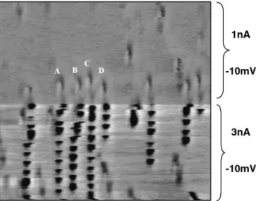
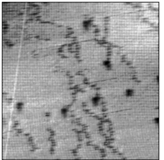
Figure 1 shows an image where the tunnel current is changed from 3 to 1 nA halfway up the scan. In the ®rst, lower part of the image (3 nA), most of the Br adsorbates appear as a series of tracks, perpendicular to the line scan. In the upper (1 nA) part of the image, the Br atoms are in ®xed, well de®ned locations on the surface. The tracks in the lower part of the image are in fact single atoms being driven in front of the tip, and hopping from one Cu surface site to another. Figure 2 is the same surface region just afterwards, but with a current of 1 nA, which is below the threshold to induce motion. The atoms marked ABCD are seen to be still in the same place as they were left in Fig. 1, but the area below them has been `swept' clear of most Br adsorbates. For 95% of our images, the underlying metal lattice has a corrugation too small to observe, as is expected for low-index metal surfaces15; but occasionally a tip structure
occurs which enables the metal atoms to be seen15. We ®nd that
the tip structure makes no signi®cant difference to the general character of the Br motion we observe. Therefore, in the remaining ®gures we show these rather rarer types of image where the metal lattice can be seen, to make the local nature of the atom motion completely clear.
The image shown in Fig. 3, taken at 2 nA, clearly shows the underlying Cu(001) lattice registry. Most atoms are hopping
Figure 1 STM image, 60 AÊ ´ 60 AÊ, of Br on Cu(100). The tunnel current is reduced halfway up the image. The tracks in the 3-nA (lower half) area are single atoms hopping from site to site. When the current is reduced the bromine atoms stop moving, for example those marked A,B,C and D.
² Present address: Department of Physics, Bilkent University, 06533 Ankara, Turkey.
letters to nature
744 NATURE|VOL 404|13 APRIL 2000|www.nature.com
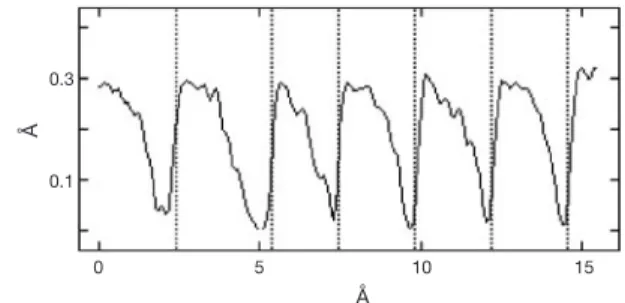
between nearest-neighbour sites in the {110} direction most nearly normal to the line scan direction. The line scan in Fig. 1 is along [110], producing essentially straight tracks, whereas in Fig. 3 it is slightly misoriented from [110], giving zigzag tracksÐmost indi-vidual hops are along [11Å0] but some are along [110]. Aligning image line scans along {100} produces fairly even zigzag tracks at 458 to the scan line. The form of the hopping motion of a single atom is shown in more detail in a line section of the image along one of the hopping paths (Fig. 4). The bromine is imaged as a depression in the surface, so as the tip nears the atom its track lowers towards the surface. At a critical separation the Br jumps away from the tip, so the tip then jumps back out to the normal height above the Cu surface. The process is similar that described by Meyer et al.10for
carbon monoxide on Cu at 30 K.
We conclude from all the above that the atoms are pushed (repelled) by the tip along the easiest available {110} direction. As might be expected, this is the direction with the lowest diffusion barrier to motion. The motion resembles a `cut' or `sliced' shot in billiards. The atom moves at nearly right angles to the direction of tip scan, because the tip's closest-approach distance to the Br atom increments in the direction normal to the raster line scan.
It might be thought that all that is now required to move an atom to a speci®ed location is to move the tip towards the atom from the opposite direction with a tunnel current above the threshold. This is much more dif®cult at room temperature than at cryogenic tem-peratures, because minute drifts of tip position between the time of the prior imaging (below threshold, to see what is to be manipu-lated) and the manipulation stroke itself, cause the tip to approach off-centre to the atomÐand hence to risk either an undesired sideways jump or even a complete miss.
We have solved this problem by modifying the motion-inducing stroke to include a small rapid `dither' perpendicular to the stroke direction. The stroke thus locally replicates the effect of the image line scan on a single atom. Figure 5 shows the `before' and `after' images of such a stroke on the marked atom. It has been deliberately displaced by ®ve lattice spacings, and this can be done in a controlled manner over any chosen, programmed distance. Clearly, the size of the lateral dither affects the proximity to which groups of atoms can be laterally positionedÐat present, this is within a couple of nearest-neighbour spacings. A thermally highly stable STM, with a smaller and more carefully shaped lateral dither
pattern, should permit very close atom placement at room tem-perature and above.
For a given tip, the threshold current required to induce atom motion was remarkably stable and reproducible. Even for different tips, and hence different appearances of the metal and Br atoms, the value always lay between 1 and 6 nA. We found that the tips that had the highest threshold currents also gave the smallest adsorbate image corrugations below the threshold. Small image corrugation suggests blunter tips, hence a larger area over which the tunnel current is spread and thus a lower current density at a single atom site. This suggests that the threshold at an atom might be governed by current density at that atom rather than just total tip±surface current.
Varying the tunnel parameters produced some interesting effects. (1) The polarity of voltage between tip and surface had no discernible effect on the threshold current for motion: the polarity could even be reversed during motion, with no apparent effect. This implies that ®xed dipoles at the surface have no signi®cant role. (2) Increasing the imaging voltage also did not detectably affect the threshold current. Images were taken at 1 nA and tip biases varying between 5 mVand 400 mV, and at none of these biases was any atom motion induced. The forces on induced atom dipoles depend on ®eld squared, so there should be a very substantial change in tip-®eld-induced polarization forces over this voltage range, but noth-ing was in fact seen. (3) In contrast, in the same experiments, if the current was increased to 3 nA, the atoms always moved, irrespective of tip voltage. Taken together, these results strongly imply that the electric ®eld between tip and surface is not directly responsible for the observed induction of motion.
More surprisingly, halving the voltage at constant current during an image failed to induce motion, whereas doubling the current at constant voltage during the same image did induce motion. Because in both cases the tip±surface separation should be reduced by a roughly similar amount, this implies that the actual distance between tip and surface itself is not solely responsible for the onset of atom movement. That is, although there is surely an overall distance-dependent force12,13with some repulsion on the Br atom,
such short-range forces seem not to be the dominant factor in triggering individual site-to-site lateral motion. This leaves us with the actual tunnel current density as the main mechanism for
Figure 2 Image taken immediately after Fig. 1, showing the same atoms marked A,B,C and D. The area below them, swept almost clear of Br atoms, is the 3-nA area of Fig. 1.
Figure 3 STM image, 120 AÊ ´ 120 AÊ, showing most Br atoms moving across the clearly visible Cu lattice. (The image was taken at 2 nA, 10 mV.) Each individual hop is in a {110} direction.
letters to nature
NATURE|VOL 404|13 APRIL 2000|www.nature.com 745
inducing motion. We stress again that none of the above observa-tions or conclusions appear to be affected by the tip type or structure.
For two images taken of the same area at low current, with a delay of a few minutes between them, we observe that some 5±10% of the Br atoms have moved, typically by one site step. Assuming an Arrhenius prefactor of about 1013Hz, the lateral barrier to motion
can therefore be crudely estimated to be a little under 1 eV. If we raise the sample temperature by 80 8C or so for even a short time, the Br atoms all diffuse away to steps and other sinks, which also suggests that the lateral diffusion barrier is around 1 eV. Now therefore if an energy of around 10 meV, additional to room temperature energy, can be delivered to an atom from an increased tunnelling current, the hopping rate of this atom will increase to a second or so per hop. With the addition of a background tip±atom repulsion, this is suf®ciently rapid to account for the manipulation we actually observe.
Following previous workers16,17, we therefore suggest that the
tunnel current is inelastically scattered, giving vibrational excitation (heating) of the Br. The excess temperature reached by the Br atom
would then depend on the balance between the vibrational relaxa-tion rate and the energy input rate16±18.The latter is proportional to
the current, giving the behaviour we observe. An increase in current by a factor of two causes the number of adsorbed atoms moving during a single image to go from a very small fraction to more than 80%. The inelastic scattering cross-section would not vary greatly over our range of a few hundred millivolts, so that the motion onset should be largely independent of voltage and in particular of polarity, as observed. Note that when we vary the voltage in the experiments, the current remains constant. We did not use voltages below 10 meV in the motion experiments, so there is always enough energy available to excite the Br motion. Multiple excitation before relaxation is also possible17,19, which might allow use of even lower
voltages, but we do not have direct evidence to indicate this at present. We point out that all surface atoms become very unstable in general STM when the currents reach values around 100 nA.
A variety of mechanisms of atom manipulation have now been reported1,19,20. The type of mechanism acting in a particular case
depends on the atom species being manoeuvred, and more than one threshold process might be present in more complex chemical and molecular systems. Atom positioning is clearly possible at elevated temperatures, and we speculate that some chemical speci®city of manipulation mechanism might become possible, leading eventually to atom selectivity when manipulating more complex molecules or structures. M
Received 1 September 1999; accepted 9 February 2000.
1. Avouris, Ph. Manipulation of matter at the atomic and molecular-levels. Acc. Chem. Res. 28, 95±102 (1995).
2. Jung, T. A., Schittler, R. R., Gimzewski, J. K., Tang, H. & Joachim, C. Controlled room-temperature positioning of individual molecules: Molecular ¯exure and motion. Science 271, 181±184 (1996). 3. Cuberes, M. T., Schittler, R. R. & Gimzewski, J. K. Room-temperature repositioning of individual C60molecules at Cu steps: Operation of a molecular counting device. Appl. Phys. Lett. 69, 3016±3018 (1996).
4. Beton, P. H., Dunn, A. W. & Moriarty, P. Manipulation of C60molecules on a Si surface. Appl. Phys. Lett. 67, 1075±1077 (1995).
5. Lyo, I.-W. & Avouris, Ph. Field-induced nanometer-scale to atomic-scale manipulation of silicon surfaces with the STM. Science 253, 173±176 (1991).
6. Dujardin, G. et al.Vertical manipulation of individual atoms by a direct STM tip-surface contact on Ge(111). Phys. Rev. Lett. 80, 3085±3088 (1998).
7. Crommie, M. F., Lutz, C. P., Eigler, D. M. & Heller, E. J. Quantum corrals. Physica D 83, 98±108 (1995).
8. Eigler, D. M. & Schweizer, E. K. Positioning single atoms with a scanning tunneling microscope. Nature 344, 524±526 (1990).
9. Whitman, L. J., Stroscio, J. A., Dragoset, R. A. & Cellota, R. Manipulation of adsorbed atoms and creation of new structures on room-temperature surfaces with a scanning tunneling microscope. Science 251, 1206±1210 (1991).
10. Bartels, L., Meyer, G. & Rieder, K.-H. Basic steps of lateral manipulation of single atoms and diatomic clusters with a scanning tunneling microscope tip. Phys. Rev. Lett. 79, 697±700 (1997). 11. Meyer, G., Zophel, S. & Rieder, K.-H. Manipulation of atoms and molecules with a low temperature
scanning tunneling microscope. Appl. Phys A 63, 557±564 (1996).
12. Jarvis, S. P., Yamada, H., Yamamoto, S.-I., Tokumoto, H. & Pethica, J. B. Direct mechanical measurement of interatomic potentials. Nature 384, 247±249 (1996).
13. Cross, G. et al. Adhesion interaction between atomically de®ned tip and sample. Phys. Rev. Lett. 80, 4685±4688 (1998).
14. Spencer, N. D., Goddard, P. J., Davies, P. W., Kitson, M. & Lambert, R. M. A simple, controllable source for dosing molecular halogens in uhv. J. Vac. Sci. Technol. A 1, 1554±1555 (1983).
15. Wintterlin, J. et al. Atomic resolution imaging of close-packed metal surfaces by scanning tunneling microscopy. Phys. Rev. Lett. 62, 59±62 (1989).
16. Ralls, K. S., Ralph, D. C. & Buhrman, R. A. Individual-defect electromigration in metal nanobridges. Phys. Rev. B. 40, 11561±11570 (1989).
17. Walkup, R. E., Newns, D. M. & Avouris, Ph. Role of multiple inelastic transitions in atom-transfer with the scanning tunneling microscope. Phys. Rev. B 48, 1858±1861 (1993).
18. Todorov, T. N. Local heating in ballistic atomic-scale contracts. Phil. Mag. 77, 965±973 (1998). 19. Shen, T. C. et al. Atomic-scale desorption through electronic and vibrational- excitation mechanisms.
Science 268, 1590±1592 (1995).
20. Hansen, O., Ravnkilde, J. T., Quaade, U., Stokbro, K. & Grey, F. Field-induced deformation as a mechanism for scanning tunneling microscopy based nanofabrication. Phys. Rev. Lett. 81, 5572±5575 (1998).
Acknowledgements
We thank M. Welland, T. Todorov and D. Eigler for comments. The apparatus used in this work was originally funded by EPSRC.
Correspondence and requests for materials should be addressed to J.B.P. (e-mail: [email protected]). 0.3 0.1 0 5 10 15 Å Å
Figure 4 Vertical section through an image along the track of a single moving atom. The individual jumps between adjacent adsorption sites are shown. The atom motion is left to right.
Figure 5 Controlled positioning of a single atom at room temperature. The lower image is taken before, and the upper image after, a manipulation stroke on the arrowed atom. Note that the next Br atom to the right moved during the second image. Images were taken at 1 nA and 10 mV; the manipulation between images was at 3 nA.