ASSEMBLY FOR HIGH RESOLUTION
MAGNETIC IMAGING SYSTEMS
a dissertation submitted to
the department of electrical and electronics
engineering
and the institute of engineering and science
of bilkent university
in partial fulfillment of the requirements
for the degree of
doctor of philosophy
By
Rizwan Akram
August 2005
Assist. Prof. Dr. Mehdi Fardmanesh(Adviser)
I certify that I have read this thesis and that in my opinion it is fully adequate, in scope and in quality, as a dissertation for the degree of doctor of philosophy.
Prof. Dr. Do˘gan Abukay
I certify that I have read this thesis and that in my opinion it is fully adequate, in scope and in quality, as a dissertation for the degree of doctor of philosophy.
Prof. Dr. Levent G¨urel ii
Prof. Dr. Billur Barshan
I certify that I have read this thesis and that in my opinion it is fully adequate, in scope and in quality, as a dissertation for the degree of doctor of philosophy.
Assoc. Prof. Dr. Ahmet Oral
Approved for the Institute of Engineering and Sciences:
Prof. Dr. Mehmet Baray
Director of the Institute of Engineering and Sciences iii
AND SQUID INTEGRATION ASSEMBLY FOR HIGH
RESOLUTION MAGNETIC IMAGING SYSTEMS
Rizwan Akram
Ph.D. in Electrical and Electronics Engineering Supervisor: Assist. Prof. Dr. Mehdi Fardmanesh
August 2005
Superconducting QUantum Interference Devices or SQUIDs are by far the most sensitive devices known for sensing magnetic flux down to a resolution of about 10−21Wb and finds innumerous applications in various fields. In order to
apply these sensors to sense nano structures or to use in antibody or antigen ammunoassay experiments, especially in unshielded environments at Liquid Ni-trogen temperatures, one needs to optimize the SQUIDs for high SNR and low background magnetic field sensitivity. The chief motivation for this research work and this thesis is to optimize and characterize HTc rf-SQUIDs so that high field sensitivity and high spatial resolution could be obtained.
During the course of this study, rf-SQUIDs were fabricated using SEJ and Bi-crystal technology and optimized for the above mentioned characteristics. In the next stage, these optimized sensors were integrated into an imaging system after a thorough investigation on problems related to the front-end assembly of such a system. Different SQUID microscope systems have been designed, fabricated, and tested in order to achieve high field sensitivity and high spatial resolution magnetic imaging under the constraint of keeping the sample at room tempera-ture, while the SQUID is in Liquid Nitrogen Temperature. Using the developed systems, magnetic imaging of room temperature samples with sensitivities in the range of about 100f T /√(Hz) and spatial resolution of about 100 µm were achieved.
Keywords: Superconductor, YBCO, Josephson Junction, Step Edge junction,
Bicrystal junction, rf-SQUID, Scanning SQUID microscope. iv
Rizwan Akram
Elektrik ve Elektronik M¨uhendisli˘gi, Doktora Tez Y¨oneticisi: Yrd. Do¸c. Dr. Mehdi Fardmanesh
A˘gustos 2005
S¨uperiletken Kuantum Giri¸sim Aygıtları veya SQUID’ler, manyetik alan algılamada yakla¸sık 10−21Wb ¸c¨oz¨un¨url¨ukle ¸simdiye kadar bilinen en hassas
aygıtlardır ve ¸ce¸sitli alanlarda sayısız uygulamaları bulunmaktadır. Bu sens¨orleri ¨ozellikle sıvı nitrojen sıcaklı˘gında koruyucu kılıfı olmayan ortamlarda, nano yapıları algılamak amacıyla uygulamak veya antikor-antijen belirleme deney-lerinde kullanmak i¸cin, SQUID’lerin y¨uksek SNR ve d¨u¸s¨uk arka plan manyetik alan duyarlılı˘gına optimize edilmesi gerekmektedir. Bu ara¸stırma ¸calı¸sması ve tez i¸cin ana ama¸c, HTc rf-SQUID’lerin karakterizasyonu ve optimize edilmesi sonu-cunda y¨uksek alan duyarlılı˘gı ve y¨uksek uzaysal ¸c¨oz¨un¨url¨ul¨u¨un elde edilebilme-sidir.
Bu ¸calı¸sma s¨uresince rf-SQUID’ler, SEJ ve Bi-kristal teknoloji kullanılarak ¨uretilmi¸stir ve yukarıda bahsedilen karakterizasyonlar i¸cin en iyi ¸sekilde op-timize edilmi¸stir. Bir sonraki adımda, optimize edilmi¸s sens¨urler b¨uyle bir sistemin kurulumundan ¨unce ve sonrasına ba˘glı olarak problemlerin tamamen ara¸stırılmasından sonra bir g¨ur¨unt¨uleme sistemine entegre edilmi¸stir. SQUID sıvı azot ortamındayken, ¨urnek oda sıcaklıı sınırlarında tutularak, y¨uksek alan has-sasiyeti ve y¨uksek uzaysal ¸c¨oz¨un¨url¨ukl¨u manyetik g¨or¨unt¨u elde edebilmek amaıyla farklı SQUID mikroskop sistemleri tasarlanmı¸s, ¨uretilmi¸s ve test edilmi¸stir. Geli¸stirilen sistemleri kullanarak oda sıcaklı˘gındaki ¨orne˘gin manyetik g¨or¨unt¨us¨u yakla¸sık olarak 100f T /q(Hz) sınırı i¸cerisinde bir hassasiyetle ve yakla¸sık 100µm uzaysal ¸c¨oz¨un¨url¨uk elde edilmesi ba¸sarılmı¸stır.
Anahtar s¨ozc¨ukler : S¨uperiletken, YBCO, Josephson kav¸sak, Step Edge kav¸sak,
Bi-Kristal Kav¸sak, rf-SQUID, SQUID tarama mikroskoplar. v
It is my pleasure to express my sincere gratitude to my supervisor, Dr. Mehdi Fardmanesh for his invaluable guidance, encouragement, and support throughout this endeavour. I am deeply indebted to him.
I would like to thank the members of my thesis committee, Prof. Do˘gan Abukay, Prof. Levent G¨urel, Prof. Billur Barshan, and Prof. Ahmed Oral for reading and commenting on this thesis.
I am obliged to thank my co-researchers in Forschungszentrum J¨ulich (Ger-many), Dr. H.-J. Krause, Dr. J. Schubert, Dr. Yi Zhang, Dr. M. Bick, Mr. M. Banzet, Mr. D. Lomparski, Mr. W. Zander, Mr. M. Schmidt, and the rest of the group for their constant support, suggestions, and help in making the setup and in the developing the devices. It would be an understatement to say that I learnt a lot from them.
I am thankful to BMBF, The German Ministry of Education and Research, and T ¨UB˙ITAK, The Scientific and Technological Research Council of Turkey, for sponsoring the joint project with Forschungszentrum J¨ulich.
Special Thanks to the Advanced Research Laboratory (Physics Department, Bilkent Univ.), for providing Liquid Nitrogen during innumerous occasions.
I would also like to thank S. Ersin Ba¸sar and Erg¨un Hırlako˘glu, Lab Tech-nicians, for their continuous help in establishing the electrical and mechanical setups.
I also thank my friends inside and outside the department, especially Ali Bozbey and Anirudh Srinivasan for their help and support.
I would like to express my deepest gratitude to S. Imaduddin Qadri, Dr. S. Fakhre Mahmud and Dr. S. Iftekhar Ahmed and their families for their relentless encouragement and moral support during all of my endeavors. Last, but not the least, I thank my family for their understanding, love, and countless prayers.
1 Introduction and Literature Survey 1
1.1 Introduction . . . 1
1.2 Thesis Organization . . . 3
1.3 Requirements for SQUID magnetic imaging . . . 4
1.4 Josephson Junction . . . 6
1.4.1 Introduction . . . 6
1.4.2 Josephson effect . . . 7
1.4.3 Circuit model and the damping characteristics . . . 12
1.5 Superconducting Quantum Interference Devices (SQUID) . . . 16
1.5.1 rf-SQUID . . . 16
1.5.2 dc-SQUID . . . 28
1.5.3 rf-SQUID configurations . . . 30
1.5.4 rf-SQUID Electronics . . . 35
2 Fabrication and Characterization of JJ 39
2.1 Introduction . . . 39
2.2 Film Deposition by PLD . . . 40
2.2.1 Working Principle . . . 40
2.2.2 The used system specifications . . . 43
2.3 Types of the employed Junctions and their fabrication techniques 43 2.3.1 Step Edge Josephson junction (SEJs) . . . 44
2.3.2 Bi-crystal Grain Boundary Josephson junction (BGBJs) . 52 2.4 Characterization Setup . . . 53
2.5 Investigation of Current Voltage Characteristics of Josephson Junctions . . . 57
2.5.1 I − V Characteristics of Step Edge Junctions . . . . 57
2.5.2 I − V characteristics of Bi-crystal Grain boundary junctions 62 2.6 Investigation of Magnetic Field Dependent Characteristics of JJ . 66 2.6.1 Principles . . . 66
2.6.2 Characteristics of SEJs under applied magnetic field . . . . 67
2.6.3 Characteristics of BGBJs under applied magnetic field . . 74
3 rf-SQUID Fabrication and Characterization 76 3.1 Introduction . . . 76
3.2 Fabrication techniques and important parameters . . . 77
3.2.2 Bi-Crystal grain boundary Junction rf-SQUID . . . 82
3.2.3 SQUID-junction characterization methodology . . . 84
3.3 Characterization setup . . . 87
3.4 Measurements and Analysis of SEJ YBCO rf-SQUIDs . . . 90
3.4.1 Step structure and JJ width dependence of SQUID charac-teristics . . . 90
3.4.2 Step height dependence of SQUID characteristics . . . 91
3.4.3 Film properties dependence of SQUID characteristics . . . 93
3.4.4 1/f noise and the temperature dependence of the noise characteristics of SEJ SQUIDs . . . 94
3.4.5 Magnetic Field Dependence of SEJ SQUIDs . . . 95
3.5 Measurements and Analysis of Bi-crystal YBCO rf-SQUIDs . . . 99
3.5.1 General characteristics related to working temperature and 1/f noise . . . . 99
3.5.2 Magnetic field dependence of bi-crystal based SQUIDs . . 100
4 Impediments and solutions for SSM 103 4.1 Introduction . . . 103
4.2 System Oriented Hurdles . . . 104
4.2.1 rf-coupling techniques . . . 104
4.2.2 Effect of LC tank circuit . . . 109
4.2.4 Effect of high frequency electromagnetic interference . . . 111
4.3 Sensor Oriented Hurdles . . . 112
4.3.1 Substrate selection (literature survey) . . . 112
4.3.2 SQUID sensor selection . . . 114
4.3.3 Effect of substrate thickness . . . 115
4.3.4 Shielding effect . . . 117
4.3.5 Flux transformer . . . 121
5 SSM Design and results 124 5.1 Introduction . . . 124
5.2 Cryostat Assembly . . . 125
5.2.1 Mobile Glass-Fiber Cryostat based system . . . 126
5.2.2 Stainless steel Cryostat based system I . . . 129
5.2.3 Prototype system II . . . 133
5.3 Scanning Results . . . 143
5.3.1 Wire scanning . . . 143
5.3.2 Dipole scanning . . . 154
6 Summary and Conclusion 158 6.1 Summary . . . 158
6.2 Conclusion . . . 164
6.3.1 Journal Publications . . . 166 6.3.2 Conference Contributions . . . 167 6.3.3 Patent . . . 169
1.1 Left; Fermi levels in two isolated metals with different work func-tions. Right; Energy levels in metal-insulator-metal junction with a bias V applied to left side. . . . 7 1.2 Schematic of Josephson junction with the wave function
represen-tations in the barrier region. . . 8 1.3 I − V characteristic for a Josephson junction at T = 0K. the
maximum zero-voltage current is equal to the normal-state current at π/4 of the quasiparticle tunneling gap. . . . 10 1.4 Rectangular shape under consideration. Dependence of the
max-imum zero-voltage current in a junction with a current density of the Fraunhofer pattern for uniform junctions. . . 12 1.5 Equivalent circuit model for RCSJ . . . 13 1.6 (a) Normalized I − V characteristics for a Josephson junction
de-scribed by RCSJ model under over-damped and under-damped cases. (b) Time dependence of current through the Josephson junc-tion for small βcat three different points on the I−V characteristic.
The average values of these functions measure the difference of the
I − V characteristics from that for βc = ∞, where only the current
through G determines the average voltage. . . . 15 1.7 Normalized I − V characteristic for a junction with βc= 4. . . . 16
1.8 a) SQUID coupled to the tank circuit via a mutual inductance M. b) Equivalent circuit of SQUID coupled to the tank circuit. . . . 17 1.9 The rf-SQUID: (a) Normalized total flux ΦT/Φ0 vs normalized
applied flux Φ/Φ0 for different βL0 values. (b) Total flux ΦT vs.
applied flux Φ for rf-SQUID with LI0/Φ0 = 5/4, showing
transi-tions between quantum states in absence of thermal noise as Φ is increased and subsequently decreased. . . 21 1.10 Peak rf voltage, VT, across tank circuit vs. peak rf current, Irf,
in absence of thermal noise for Φ = 0 (solid line) and Φ = ±Φ0/2
(dashed line). . . 22 1.11 Tank circuit voltage, VT, vs rf drive current IT for four values of the
tuning parameter δ = [2(ωrf − ω0)/ω0]Q and for Φ = 0, andΦ0/2.
Curves plotted for κ2Qβ0
L = π/2 (Hansma, 1973).) . . . 25
1.12 ² vs. L/Lth0 for nonhysteretic rf-SQUID at 77K (chesca, 1998). . 27
1.13 The dc-SQUID: the symbol (left) and the equivalent circuit (right). 28 1.14 The current voltage characteristics at low extreme flux values (left)
and output voltage vs. applied flux (right). . . 29 1.15 A typical schematic for rf-SQUID readout electronics. . . 36 1.16 The effect of externally applied low frequency signal flux together
with rf power flux. . . 37 2.1 A schematic diagram of the PLD system: (1) Target, (2) substrate
(heated by direct joule heating), (3) ablated species “Plume,” (4) focused laser, (5) electron probe, (6) diffracted electrons, (7) elec-tron gun, (8) phosphorous screen, (9) CCD camera, (10) focusing lens, (11) ultra high vacuum chamber, (12) substrate manipulator, (13) target manipulator [1]. . . 41
2.2 Steps involved in the formation of ditch on the substrate for SEJ formation. . . 46 2.3 Stepwise explanation of the device fabrication process. . . 49 2.4 SEM pictures of step structures on LaAlO3 substrates; a) etched
using normal incident ion beam (left), b) etched using ”Combina-torial IBE” process(right) . . . 51 2.5 Characterization setup using liquid Helium/Nitrogen as coolant. 54 2.6 Temperature dependence of I − V curve versus bias current of the
junction of an rf-SQUID magnetometer made on LaAlO3substrate
with 260nm deep CIBE steps. . . 58 2.7 Temperature dependence of dynamic resistance (dV/dI) versus
bias current of the junction of an rf-SQUID magnetometer made on LaAlO3 substrate with 260nm deep CIBE steps. . . 59
2.8 I−V characteristics and corresponding dV/dI at ∼ 10K of the 2µm wide SEJ of an rf-SQUID magetometer made on LaAlO3 substrate
with 255nm deep steps. . . 60 2.9 Typical temperature dependence of I − V characteristics of a
RSJ-type Single SEJ on 260nm deep step (3µm wide) . . . . 61 2.10 Typical temperature dependence of dynamic resistance of a
RSJ-type single SEJ on 260nm deep step (3µm wide) . . . 62 2.11 Typical temperature and junction width dependence of critical
cur-rent of SEJs on a 200nm deep ditch on LaAlO3 substrate. . . 63
2.12 I − V and dV/dI curves of 3-8µm wide BGBJs on 36.8o bicrystal
SrT iO3 substrate. . . 64
2.13 Effect of junction width on the dV/dI characteristics at low tem-perature of 7K. . . 65
2.14 Effect of junction width on the dV/dI characteristics at high tem-perature of 63K. . . 66 2.15 Classical magnetic field dependence of Ic of both type of the
junc-tions. . . 67 2.16 Effect of applied field on the critical current, Ic, and temperature
dependence of junction of rf-washer SQUID measured after open-ing the SQUID washer loop. . . 68 2.17 Field Dependence of the Vsppof rf-SQUID whose junction is shown
in Figure 2.16. . . 69 2.18 Magnetic field dependence of the I − V and dV/dI curves for a
high field-sensitive 1µm wide junction made on CIBE step. . . . . 70 2.19 Magnetic field dependence of the I − V curves of a low
field-sensitive 3µm wide junction made on 260nm deep CIBE steps. . . 71 2.20 The applied magnetic field dependence of a field dependent 3µm
wide junction. . . 72 2.21 Applied magnetic field dependence of the 8µm wide junction versus
bias current at various temperatures (top:) Low and (bottom:) high temperature limits. . . 73 2.22 Magnetic field dependence of Ic of 3, 5, and 8µm wide GB
junc-tions on bi-crystal SrT iO3 substrates. The calculated classical
field dependence of the Ic is shown for the 8µm wide junction. . . 74
2.23 The applied magnetic field dependence of the 8µm wide junction versus bias current at various temperatures. The measured field dependence closely follows the calculated magnetic field modula-tion at all temperatures. . . 75 3.1 SEJ rf-SQUID gradiometer layout. . . 78
3.2 SEJ rf-SQUID magnetometer. . . 79 3.3 SEJ structure and the asymmetric grain boundary junctions shown
for a rf-SQUID magnetometer.[2] . . . 80 3.4 Chip layout of the SEJ magnetometers with separate SEJs in
dc-SQUID configuration in order to characterize the junctions for dc characteristics in parallel to rf-SQUID characterization [2]. . . 81 3.5 Asymmetric rf-SQUID layout design of tri-junction gradiometer. [3] 83 3.6 Asymmetric rf-SQUID layout design of bi-junction magnetometer.[3]
84
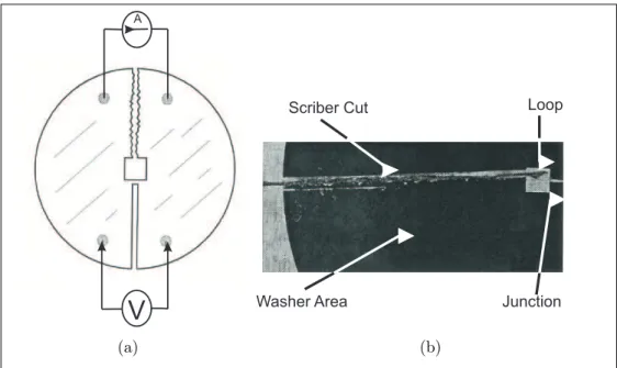
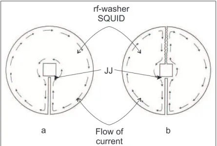
3.7 (a) Schematic diagram of an rf-washer-SQUID with open ring and ohmic contacts for characterization of I −V characteristics in four-probe configuration. (b) A photograph of the washer of SQUID, which is mechanically opened using diamond scriber. . . 85 3.8 Schematic sketch of the current flow in a) SQUID and b) SQUID
with opened SQUID washer area . . . 86 3.9 Schematic sketch of the measurement setup for the characterization
of rf-SQUID at liquid Nitrogen/Helium temperatures. . . 88 3.10 Vspp vs. T of SQUIDs made of 200nm thick YBCO films on
LaALO3 substrates with CIBE steps. The solid lines show the
Vspp of 2-5 µm wide junction gradiometers for step heights of 230
nm (rigt) and 280 nm (left). The dashed lines show the Vspp of 3
3.11 Flux to voltage transfer function signal, Vspp, versus temperature of
rf-SQUID magnetometers with 100 µm × 100 µm loops. “SQUID 2” has a 205nm deep ditch and SQUIDs 3 and 4 have 135nm deep ditches, made using the optimized CIBE process. “SQUID 1” has a 275nm deep ditch, made using un-optimized CIBE process. The junction width of “SQUID 3” is 2 µm, and the other devices have 3 µm wide junctions [5]. . . . 92 3.12 The noise spectra of the sample measured at liquid Nitrogen
tem-perature using conventional LC tank circuit [5]. . . 93 3.13 a) Normalized magnetic field dependence of Vspp of a high
field-sensitive 2µm wide junction SEJ rf-SQUID b) Magnetic field de-pendence of Vspp versus temperature of a low field-sensitive SEJ
rf-SQUID. . . 96 3.14 Magnetic field dependence of Ic of the junction of high
field-sensitive rf-SQUID at low and high temperatures. . . 97 3.15 Noise spectra of rf-SQUIDs with high field-sensitivity (SQUID 1)
and low field-sensitivity (SQUIDs 2 and 3) characteristics. SQUID 3 is measured in liquid Nitrogen using optimal LC tank circuit. . 98 3.16 Magnetic field dependence of flux voltage transfer function signal,
Vspp, of asymmetric junction bicrystal-GB rf-SQUID. . . 101
4.1 Direct coupling limitations due to size of the capacitor and coupling coil. . . 105 4.2 A flip chip configuration for rf-SQUID and circular coplanar
res-onator with integrated flux concentrator. . . 106 4.3 Possible coupling configurations between SQUID and the coplanar
4.4 Noise spectra of low 1/f noise rf-SQUID magnetometer measured with conventional L-C tank circuit and superconducting coplanar resonator. The field sensitivity of the bare SQUID at white noise level is 170f T /√Hz. . . 108
4.5 Effect of shielding on the maximum SQUID signal level under shielded condition with different rf coupling techniques. . . 109 4.6 Effect of LC tank circuit on the SQUID signal level, where tank
circuit 1 has small and tank circuit 2 has large loop diameters for the inductor. . . 110 4.7 Effect of shield area on Vspp and period of SQUID signal vs. the
employed electronics (electronics 1 = 1 GHz, electronics 2 = 400 to 700 MHz). . . 111 4.8 Noise spectra of bicrystal GB magnetometer and gradiometer
de-signs on bicrystal SrT iO3substrate at their optimal operating
tem-peratures. . . 114 4.9 Conceptual picture for substrate thinning effect. . . 115 4.10 Effect of substrate thickness between SQUID and LC tank circuit. 116 4.11 Schematic illustration of application of shield with width, W , and
length, L; the thickness of the YBCO shielding film was 200 nm. 118 4.12 Determination of shielding factor. . . 118 4.13 Effect of shield area on Vspp and period of the SQUID signal. . . 119
4.14 Effect of the tank circuit, while measuring the effect of shielding on the SQUID characteristics. a) Tank circuit 1 and 2 are conven-tional LC tank circuits but the loop diameter of inductor for tank circuit 1 is small compared to the tank circuit 2. b) Resonator circuit. . . 120
4.15 Effect of working temperature range on the shielding area. . . 121 4.16 Conceptual figure for the new configuration for the sensing setup
with SQUID coupled to the transformer face to face. . . 122 5.1 (a) Mobiler Kryostat ILK 2 with cold finger. (b) Top view of the
Dewar. . . 127 5.2 (Left:) Cooling capacity vs. temperature of Kryostat. (Right:)
Hold time vs. temperature of Mobiler Kryostat ILK 2 dewar. . . 128 5.3 Schematic of the SQUID microscope with stainless steel cryostat. 129 5.4 Sketch of the dewar [6]. . . 130 5.5 Sapphire cold finger with a diameter of 14mm. The upper hole
serves as a fixture for the Pt-100 for temperature control. The coaxial measurement cable for the SQUID is guided through the inclined longitudinal hole with the opening at the side of the sap-phire. . . 131 5.6 Schematic diagram of the hand made scanning SQUID microscope
system. . . 134 5.7 Three-layer µ-metal shield with circular shape, used to shield
against low frequency magnetic filed. . . 136 5.8 Faraday cage made with aluminium sheet of thickness of about 0.5
mm to shield against high frequency EM waves. . . 137 5.9 Scanning Stage configuration for microscope design. . . 139 5.10 Styrofoam Dewar design and sample holder configuration for
pro-totype system. (a) schematic diagram of the dewar (b) dewar with its accessories (c) glass configuration and (d) sample holder. . . . 140
5.11 Front pannel of the LabView program developed to take the data and control the scanning stage. . . 141 5.12 Block diagram representing the setup for sensing the dipole motion
by computer controled system. . . 142 5.13 Principal setup for detection of magnetic field from a moving wire
with an ac current modulation. . . 143 5.14 Results of magnetic distance measurement and fitting data with
approximate model. . . 144 5.15 Results of magnetic distance measurement and fitting data with
approximate model. . . 147 5.16 Ultimate field resolution for the system, which is quite linear
pre-dicting that the resolution can be increased further, if we decrease the distance between the sample and the SQUID. . . 148 5.17 Schematic illustration of transformer coupling mechanism in order
to improve the spatial resolution of SSM. . . 149 5.18 Results of magnetic distance measurement and fitting data with
approximate model. . . 150 5.19 Conceptual diagram for the Expected SQUID response for the
scanning of wire with an ac current regarding the position of the wire with respect to the center of the gradiometer. . . 151 5.20 Effect of applied field to find the field resolution of the system. . 152 5.21 Effect of direction of the current on the response of the SQUID. . 152 5.22 Finding the ultimate field resolution for wire scanning sample; (a)
when the current through the wires are in the same direction, (b) when the current direction in the wires are apposite with respect to each other. . . 153
5.23 Visualization of a magnetic particle by the use of small loop of fixed diameter; where wire twisting has been used to decrease the effect of wires. . . 154 5.24 Field resolution by using 150µm diameter dipole configuration with
a distance of about 2 mm between the sample and the SQUID. . 155 5.25 Maximum achieveable field resolution with 1.2 mm distance
be-tween the SQUID and the sample. . . 156 5.26 Effect of applied current direction and the separation between two
4.1 Possible SQUID and the coplanar resonator coupling configura-tions with their relative signal and signal locking states. (S: SQUID, R: Resonator, sub: substrate, C: pick up coil electron-ics) . . . 107 4.2 Lattice parameters for the YBCO and the related substrate
com-pounds. . . 113 4.3 Substrate thickness effect on the Vspp. Here the ratios have been
taken by dividing the maximum signal level which is at optimum thickness level, to either 0mm (direct) or 1mm (indirect) coupling. 117 5.1 Basic shielding materials and their general properties . . . 136
Introduction and Literature
Survey
1.1
Introduction
Effect of magnetism is known from ancient times for about more than 4000 years. But till 19th century, it was just used as compass for medieval explorers to
nav-igate [7]. Though, discovery of the first quantitative magnetometers was late till 19th century, application of magnetic sensors today has a wide range such as
metrological, domestic and industrial proximity switching, electromagnetic non-destructive testing, geomagnetic, and prospecting a biomagnetism [8].
Two inherently different types of magnetic sensors exist: absolute and vector-ial. Absolute magnetometers are based on Zeeman effect and are scalar magnetic field-to-frequency converters, measuring the absolute values of the field, regard-less of the orientation, with field sensitivities of few pT /√Hz with bandwidth
of 1 Hz to 1kHz [9], [10]. Whereas for vectorial sensors, projection of the field vector onto the sensitive direction of the device is measured. As the magnetic flux penetrating a pickup area is detected, they can be regarded as magnetic flux-to-voltage converters. In this case, field sensitivities of a few pT /√Hz with
about 1000 Hz bandwidth are attainable [11]. Hall probes [12] and conventional 1
magnetoresistors are based on galvanomagnetic effects occurring in semiconduc-tors and metals [13], [14]. Field sensitivities of Hall probes lie in the range of a few hundred nT /√Hz. Whereas field sensitivity in magnetoresistive sensors,
based on carrier scattering with the lattice results in the increased electrical path length causeing a change in the electrical resistance, typically range around a few hundred pT /√Hz. For low-field sensitivity, high-permeability ferromagnetic
Ni-Fe alloys and flux focusers are employed [15]. This way record sensitivity values down to 1pT /√Hz have been reported. In addition to sensitivity limitations of
each of the sensors described above, limitations in spatial resolution, dynamic range, linearity, bandwidth and the thermal and temporal stability have to be taken into account.
In terms of detectability of localized weak dipoles, the flux sensitivity is the figure of merit of the sensor. The SQUID ”Interferometers or superconducting quantum interference devices (SQUIDs)” is by far the most sensitive sensor of magnetic flux known, reaching a resolution of 10−21 Wb. Magnetic field
resolu-tion in the range of f T /√Hz are possible with a pickup area of only few square
millimeters. Magnetic flux quantization in the superconducting loop and the Josephson effect lead to a flux-to-voltage characteristic with flux quantum peri-docity. Hence, an extremely large dynamic range is attainable, especially when combining a null-detector scheme with flux quanta counting. The only major draw back of SQUIDs is that they require cooling to very low temperatures, with the attending relatively high cost and somewhat complicated handling.
SQUID works on the basis of interference of the superconducting wave func-tion across a juncfunc-tion called the Josephson juncfunc-tion. It is a deceptively simple device, consisting of a small superconducting loop of inductance Ls with one or
two damped (resistively shunted, RSJ) Josephson junctions, each having a critical current, Ic, and normal resistance, Rn. Magnetic flux threading the
supercon-ducting loop is always quantized in units of Φ0, where Φ0 = 2.0679 × 10⁻⁵Wb
is the flux quantum. The phase difference across a Josephson junction switches by 2π when its current crosses Ic. In brief, the junction is shortening the
sin-gle junction SQUID by a superconducting path; therefore, the voltage response is obtained by coupling the loop to a radio frequency biased tank circuit. For
this reason this kind of devices is usually called an rf-SQUID, which is further discussed later in this chapter. In the double junction configuration, the weak links are not shorted by a continuous superconducting path; therefore, the dc current-voltage characteristics can be observed. In the operating conditions, the device is current biased at a value slightly greater than the critical current, and the voltage drop across it is monitored. These kinds of devices are usually called dc-SQUIDs.
Here, we will analyze the rf-SQUID in details as during the course of this study rf-SQUID has been the basic sensor for the targeted scanning SQUID microscope, used either in magnetometer or gradiometer configuration. Both configurations will be discussed in detail later in this chapter.
1.2
Thesis Organization
The first chapter of this thesis discusses the basic requirements for developing the high resolution imaging system using Optimized SQUID sensor and SQUID integration assembly. The necessary literature survey on the basic components of a SQUID sensor, its working principle, and some necessary formulations to be able to follow the discussions in the forthcoming chapters are also included.
The second chapter discusses Josephson junctions in detail, starting from fab-rication techniques, and the characterization setup to the individual characteris-tics of Step Edge Junctions and Bi crystal grain boundary Josephson junctions. This is based on the I − V characteristics and magnetic field dependencies of these particular junctions.
Chapter 3 is on the rf-SQUID sensors. In this chapter we discuss in rigor-ous detail the important issues related to the fabrication and optimization of rf-SQUIDs for high resolution magnetic imaging systems.
The impediments related to the front end assembly of microscope is discussed in chapter 4. The expected solutions to these problems have also been discussed
in details in this chapter.
Chapter 5 includes the developed and investigated systems for scanning SQUID microscopy with advantages and disadvantages together with scanning results on wire samples and dipoles to find out the ultimate field and spatial resolution of the developed prototype system.
Summary and conclusions are presented in chapter 6 together with the scien-tific contributions of this work and some suggestions for future work for improving the spatial resolution by using multi layer self shielded transformer structures.
1.3
Requirements for SQUID magnetic imaging
To make a SQUID microscope we need to optimize the SQUID properties for stability of working in the desired temperature range while having low noise as well as background field independence. What we need as a first site is to have high temperature Superconductor, HTS, junctions which have the highest possible
IcRn product at 77K in the range between 0.1 and 1 mV, to provide high Vspp at
this temperature. Higher IcRn value conforms high signal to noise ratio (SNR).
Of the many types of internally shunted HTS Josephson junctions, which have been investigated and developed in the past decade, only some can approach these requirements. The grain boundary bicrystal junction, i.e, microbridges patterned on bicrystal substrates, typically SrT iO3, have been preferentially used
by most experimenters and SQUID vendors [16], [17], [18], [19]. Other types of junctions currently used by some of leading experimental groups are: GB step-edge junctions patterned as microbridges across steep steps locally etched in substrates [20], SNS step-edge junctions with normal interlayer across the step in substrate being gold, silver or an Au-Ag alloy [21], quasi-planar SNS edge (ramp) junctions with praseodymium cuprate P rBa2Cu3O7−δ (PBCO) barriers
[22], and SNS junctions consisting of oxygen-ion implanted weak links [23]. Not used commercially, but worthy of mentioning are the CAM (c-axis microbridge) planar junctions, which unfortunately have low Rn [24].
Each of the above mentioned types, offers some advantages and disadvantages. Bicrystal junctions are the easiest to fabricate and their Ic and Rn are relatively
reproducible with spreads lower than in most other types (best 1σ = 20 to 30%). Here, they are particularly suitable for dc-SQUIDs where the Icand Rnof the two
junctions should be nearly identical. However, bicrystal substrates are expensive and impose topological limitations on the SQUID layout design, since the grain boundary extends across the whole substrate. When it intersects other parts of the superconducting layout, such as the washer body or the flux pickup loop, additional 1/f flux noise is likely to be generated in the film’s grain boundary. This boundary represents a long Josephson junction, in which Josephson vortices can easily shuttle. Another disadvantage of this method is the small integration scale of junctions since all junctions are aligned along the bicrystal boundary.
In the step-edge process, steps of thicknesses comparable to the film thickness are made in the substrate by etching. When the YBCO film is grown across the edge, the c-axis is tilted and at least two grain boundaries are formed. It has been possible to adjust the junction parameters by adjusting the step height and angle, but the junction reproducibility has been low [25]. Stepedge GB junctions use less expensive substrates and can be relatively freely positioned on the substrate (when a series connection of two junctions is acceptable), but their reproducibility is poorer and have typical spreads of parameters much larger compared to e.g. bicrystal junctions. These junctions found application mostly in rf-SQUIDs, as only one junction is required there. The Icand Rnof both mentioned GB junction
types can be easily adjusted or trimmed by annealing in oxygen, inert atmosphere, or vacuum. This is done at temperatures low enough for YBCO films properties not to be seriously affected, except at the grain boundary [26]. The Rn values
for a few microns wide junctions are typically in the 1 to 10Ω range, suitable for SQUID operation. The correlation between Icand Rn is given by the scaling law
in the form:
IcRn ∝ (1/ρn)qorIcRn∝ (Jc)
q
q+1, (1.1)
about 1.5 on SrT iO3. This scaling is generally valid for HTS junctions.
In the biepitaxy process, a thin (l0-20 nm) seed layer is deposited epitaxially on part of a substrate. During the YBCO growth, the in-plane (a − b) orientation is different for the film grown on the seed layer compared to other parts of the substrate, and hence, grain boundaries are formed at the borders. Most processes give a 45o rotation, but misorientation angles of 18o and 27o have also been
reported [27].
The SNS step-edge junctions insure a similar freedom of positioning as the GB step edge type, but the fabrication process is much more difficult and has been mastered by only a couple of laboratories [28], [29]. However, these junc-tions apparently exhibit excellent long-term stability and reasonable spreads of
Ic and Rn, comparable to those found in bicrystal junctions on SrT iO3.
Simi-larly, freedom of positioning, excellent long term stability, and acceptable spread are claimed for edge junctions with PBCO barriers, and for ion implanted SNS weak links, but again at a price of a complicated fabrication process. For SNS and ramp junctions, the typical values of Ic and Rn can be made comparable to
those of GB junctions. Today, no optimum type of junctions for SQUIDs can be identified. However, it is probable that with continuing progress in fabrication process, the GB junctions will be replaced by one or another type of SNS or PBCO barrier junctions suitable for multilayered SQUID structures [30].
1.4
Josephson Junction
1.4.1
Introduction
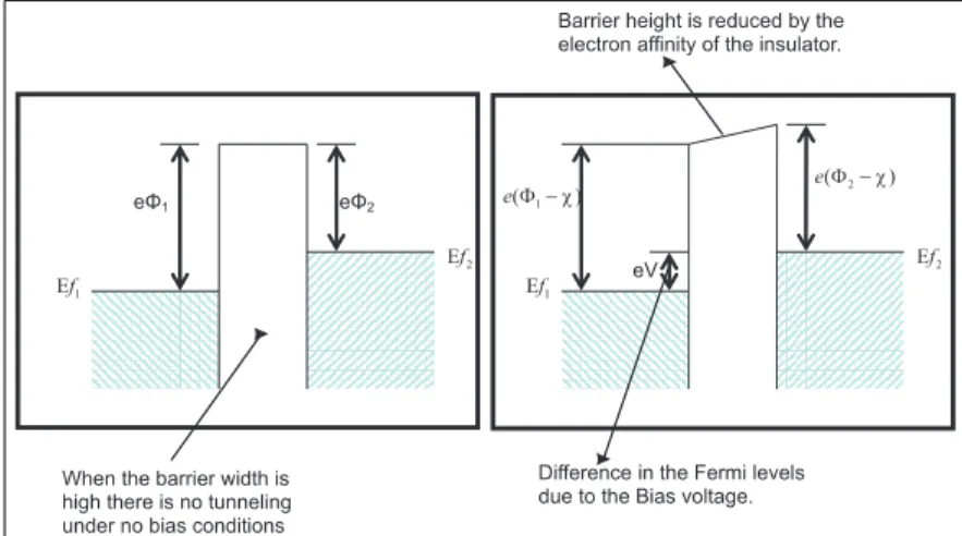
The term tunneling is applicable when an electron passes through a region, in which the potential is such that a classical particle with the same kinetic energy can not pass, as shown in Figure 1.1. In quantum mechanics, one finds that an electron incident on such a barrier has a certain probability of passing through, depending on the height, width, and the shape of the barrier.
Figure 1.1: Left; Fermi levels in two isolated metals with different work functions. Right; Energy levels in metal-insulator-metal junction with a bias V applied to left side.
There are different types of tunneling junctions which can be made, like normal-insulator-normal (NIN), normal-insulator-superconductor (NIS), and Superconductor-insulator-Superconductor (SIS). Here in this section we study the SIS type of tunnel junction before going in to the analysis of the particular GB case.
1.4.2
Josephson effect
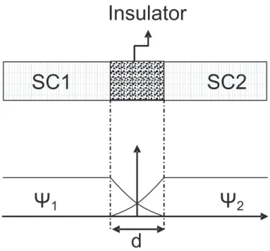
The idea of tunneling of electron pairs between closely spaced superconductors even with no potential difference was first suggested by B.D. Josephson during his PhD. in 1962. This goes back to formation of junctions between two super-conductors, which are weak enough to allow slight overlap of electron pair wave function of two individual superconductors as shown in Figure 1.2.
In addition to this so-called Josephson tunnel junction (or SIS Junction, Su-perconductor Insulator SuSu-perconductor) numerous other configurations also al-lows weak coupling between two superconductors for both metallic (LTcSC) and
oxide (HTcSC) materials. This includes thin normal conducting layer (SNS)
junctions, micro bridges, grain boundaries, damaged regions, and point contacts serving as weak contacts. The most important characteristic property of the pair
Figure 1.2: Schematic of Josephson junction with the wave function representa-tions in the barrier region.
tunneling is that, unlike quasi particle tunneling, it does not involve excitations and can occur even without bias across the junction. This refers to absence of voltage when we bias the junction with currents less than critical current where this current is carried through the junction by cooper pairs.
1.4.2.1 Josephson Relations
Wave function to describe the pairs in the superconductors can be expressed in the form as,
ψ = |ψ(r)| exp{iθ(r) − (2εf/¯h)}, (1.2)
where |ψ(r)|2 represents the actual Cooper pair density, ns. As the separation
of the superconductors is reduced, the wave functions penetrate the barrier suf-ficiently to couple where the system energy is reduced by the coupling. When this energy exceeds the thermal fluctuation energy, the phases become locked and pairs can pass from one SC to the other without energy loss. Under biased condition, the only difference between the pair tunneling is that this time phases
of wave function are not locked but rather slip relative to each other at a rate that is precisely related to the voltage. Time evolution of the wave function of the superconductor on each side of a coupled Josephson junction results in the following famous Josephson relations;
J = Jcsin φ (1.3)
where Jc is the critical current density and,
∂φ ∂t =
2e
¯hV (1.4)
These are the Josephson relations that express the behavior of the electron pairs. From these Josephson relations, it can be inferred that coupling of the wave function reduces the energy which can be expressed as,
Ec= (¯hIc/2e) cos φ (1.5)
so coupling energy is maximum when φ=0, but as the current density, J, is raised to its maximum value of Jc, φ → π/2 and coupling energy is reduced to zero. For
currents where J > Jc , the wave functions become uncoupled and begin to slip
relative to each other at a rate determined by phase equation. General expression from microscopic theory for the maximum zero-voltage current density, can be written as : Jctu = Gn A Ã π∆(T ) 2e ! tanh∆(T ) 2kBT (1.6) where Gnis the tunneling conductance for V À 2∆/e and A is the junction area.
Figure 1.3: I − V characteristic for a Josephson junction at T = 0K. the max-imum zero-voltage current is equal to the normal-state current at π/4 of the quasiparticle tunneling gap.
1.4.2.2 Josephson Ac Effect
If a dc-voltage ıV0 is applied to a junction, integration of second Josephson rela-tion shows that
φ = φ0+ (2e/¯h) V t. (1.7)
If this is substituted into current density expression we obtain,
I = Icsin(ωJt + φ0). (1.8)
So there is an ac current at the frequency,
fJ = ωJ 2π = µ 1 2π ¶2e ¯hV. (1.9)
An important aspect of this result is that substantial ac pair currents flow even when the junction voltage exceeds the gap by several times. So it can be referred
that junction under applied voltage behave like an antenna which radiates this ac current. This current can close itself through quasi particles that is the reason of putting R to its model, which will be discussed in details in the next section. Another important fact is that this ac current causes ac voltage and these ac voltages add up to that dc voltage which one wants to flow through the junction.
1.4.2.3 Magnetic field Effect
For a general shape under the assumption that magnetic field produced by tun-neling currents is negligible and the applied field is in the y direction, we can write, ∂φ ∂z = 2ed0 ¯h B o (1.10)
Here Bo is the field in the insulator region, and, d0 = d + 2λ where d is
the insulator thickness and λ is the penetration depth. By plugging the phase obtained from the above equation into Josephson relation and integrating along
y and z coordinates, we get the current per meter width as,
I(Bo) = ∞ Z −∞ Jc(z) sin " 2ed0Bo ¯h z + φ(o) # dz (1.11)
Special Case: As shown in the following figure we consider a rectangular junction with uniform critical current density. In this case, the above current integral ends up to a well known expression,
I(Bo) = I c(0) ¯ ¯ ¯ ¯ ¯ ¯ sin³ed0LBo ¯ h ´ ed0LBo ¯ h ¯ ¯ ¯ ¯ ¯ ¯= Ic(0) ¯ ¯ ¯ ¯ ¯ ¯ sin³πφφ0´ πφ φ0 ¯ ¯ ¯ ¯ ¯ ¯ (1.12)
Where the constants in the above equation are defined as Ic(0) = W LJc, e/¯h =
π/φ0, and φ = d
0lB0. Equation 1.12 is plotted in Figure 1.4 for symmetric junction
case. An important observation thus can be concluded by the measurement of maximum zero-voltage, is to find out the uniformity of the junction by comparing
with the symmetry of the sinc function of the form as derived from the above equation. But this test is valid as far we are in the limit of small junction
³
L/λj ≤ 1 ´
approximation, where self-field effect is not included.
Figure 1.4: Rectangular shape under consideration. Dependence of the maximum zero-voltage current in a junction with a current density of the Fraunhofer pattern for uniform junctions.
Now let’s assume the case when we have junctions with higher dimensions compare to λj and we face the problem of self-field effect due to the tunneling
currents. In this particular case we see that there are two important symptoms of the self-field effect; 1) Current through the junction does not increase indefinitely as the size of the junction is increased, and 2) We don’t observe zero in the maximum zero voltage for any applied value of magnetic field. Analysis of such sort of problem requires nonlinear mathematics and can be solved numerically.
1.4.3
Circuit model and the damping characteristics
Whenever we have sufficiently weak coupling between two superconductors, then Josephson relations can be applied as,
I = Icsin φ
∂φ ∂t =
2e
Though Ic(T) suffices to characterize the zero voltage dc properties of a weak
link for finite voltage situations involving the ac Josephson effect, but we de-fine the junction with its equivalent model when it is required to get complete analysis. Here this section discusses the most famous model, to describe the Josephson junction, named as RCSJ (resistively and capacitively shunted junc-tion) model, in which physical Josephson junction is modeled by an ideal current source, shunted by a resistance R and a capacitance C. This model is shown in Figure 1.5. Resistance R builds in dissipation in the finite voltage regime, without affecting the lossless dc regime, while C reflects the geometric shunting capacitance between the two electrodes and not the capacitance of the electrodes to ground. Capacitance models the presence of displacement current, which flows between the adjacent superconducting electrodes.
Figure 1.5: Equivalent circuit model for RCSJ .
Considering that above given circuit is biased with a dc current source and according to the analyses of Stewart and McCumber assuming G constant, we can write the differential equation of the above circuit of RCSJ model as,
I = Icsin φ + GV + C
dV
dt . (1.14)
Eliminating V in favor of φ, we obtain the second order differential equation,
I = ¯hC 2e d2φ dt2 + ¯hG 2e dφ dt + Icsin φ. (1.15)
If we divide the above equation by Ic and introduce a dimensionless time variables, θ = ω∆ ct= (2e/¯h) (I∆ c/G) t (1.16) and βc =∆ ωcC G ∆ = µ2e ¯h ¶ µI c G ¶C G = Q 2, (1.17)
where Q is the quality factor, then we obtain a more simplified expression for the above equation as,
I Ic = βc d2φ dθ2 + dφ dθ + sin φ. (1.18)
Where βc, damping parameter, is the ratio of the capacitive susceptance at
that frequency to the shunt conductance. ‘ωc’ is called plasma frequency or
Josephson angular frequency for a voltage corresponding to the maximum zero-voltage current Ic and the conductance G. As far as I < Ic a static solution to
above equation with φ = sin−1(I/I
c) and V=0 is allowed, but when I > Ic then
only time dependent solution exists. We have two conditions for the later case, “over damped” when C is very small, and “under damped” when C is large.
• Over damped junction: We have this condition when C is small enough
so that Q ¿ 1. This reduces the equation 1.18 to first order differential equation of the form,
dφ dt = 2eIcR ¯h µI Ic − sin φ ¶ . (1.19)
As can be seen from the above equation, the dφ/dt is always positive when
I > Ic. So the phase advances more slowly when sin(φ) is positive, and
vice versa. Hence to find the I − V relation, first we find the time average voltage by integrating this equation to determine the period of time, T , required for φ to advance by 2π. Then using the Josephson frequency relation 2eV /¯h = 2π/T we get,
V = R³I2− I2
c
´1/2
This parabolic dependence for I > Ic and βc =0 is shown in Figure 1.6(a),
where normalized voltage GV /Icis plotted in relation to normalized current
I/Ic.
Figure 1.6: (a) Normalized I − V characteristics for a Josephson junction de-scribed by RCSJ model under over-damped and under-damped cases. (b) Time dependence of current through the Josephson junction for small βc at three
dif-ferent points on the I − V characteristic. The average values of these functions measure the difference of the I − V characteristics from that for βc= ∞, where
only the current through G determines the average voltage.
It is clear that an appreciable amount of dc current is flowing through the Josephson junction at low voltages for βc = 0. If the voltage across the
junction were dc only, there would be only a sinusoidal ac current. This ac current in the junction passes through the shunt conductance as the source has infinite impedance. It thus produces an alternating voltage across the junction, so the rate of change of phase is no longer constant. Then the result is a complex temporal variation of current; as seen by averaging
V = (2π/Φ0) dφ/dt (1.21)
over one period, which has a periodicity equal to the Josephson frequency equivalent of the average voltage. Figure 1.6(b) shows how the current becomes increasingly non sinusoidal as the voltage approaches zero.
• Under damped Junction: This condition which is much complex than
the previous one arises when C is large enough so that Q > 1. In this case
Imin > I < Ic in which there are two values of voltages, V = 0 and V 6= 0.
So upon increasing I from zero, V=0 until Ic, at which point V jumps
discontinously up to a finite voltage V , corresponding to a running state, in which the phase difference increases at the rate 2eV /¯h . On the way back if I is reduced below Ic, V does not drop back to zero until a retrapping
current Ir ≈ 4Ic/πQ is reached. Hysteretic I −V curve of an under damped
Josephson junction is shown in Figure 1.7 with two different schematics for detailed understanding [31].
Figure 1.7: Normalized I − V characteristic for a junction with βc= 4.
1.5
Superconducting Quantum Interference
De-vices (SQUID)
1.5.1
rf-SQUID
The rf-SQUID consists of a single Josephson junction integrated into a supercon-ducting loop that is inductively coupled to the inductance LT of an LC resonant
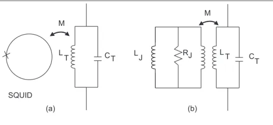
(tank) circuit [Fig. 1.8(a)]. The tank circuit is driven by an rf current, and the resultant rf voltage is periodic in the flux applied to the SQUID with period Φ0.
Detailed reviews on rf-SQUIDs have been written by many authors (for example, Jackel and Bhrman, 1975; Ehnholm, 1977; Likharev and Ulrich, 1978; Likharev, 1986; Ryhanen et al., 1989; Clarke, 1996).
Figure 1.8: a) SQUID coupled to the tank circuit via a mutual inductance M. b) Equivalent circuit of SQUID coupled to the tank circuit.
The total flux ΦT in rf-SQUID is related to the applied flux Φ by
ΦT = Φ − LI0sin(2πΦT/Φ0). (1.22)
We see immediately that Eq. 1.22 can exhibit two distinct kinds of behav-iors. For β0
L = 2πLI0/Φ0 < 1, the slope dΦT/dΦ = [1 + βL0 cos(2πΦT/Φ0)]−1 is
everywhere positive and the ΦT vs Φ curve is nonhysteretic. On the other hand,
for β0
L> 1, there are regions in which dΦT/dΦ is positive, negative, or divergent
so that the ΦT vs Φ curve becomes hysteretic. Radio frequency superconducting
quantum interference devices have been operated in both modes. In the hysteretic mode the SQUID makes transitions between quantum states and dissipates en-ergy at a rate that is periodic in Φ. This periodic dissipation in turn modulates the quality factor Q of the tank circuit, so that when it is driven on resonance with a current of constant amplitude, the rf voltage is periodic in Φ. In the case β0
L < 1, the nondissipative mode, the SQUID behaves as a parametric
of the tank circuit as the flux is varied. Thus when the tank circuit is driven at constant frequency, the variations in its resonant frequency cause the rf voltage to be periodic in Φ.
Historically, it appears that most low-Tcrf-SQUIDs were operated in the
hys-teretic mode, although as we shall see, there are advantages to the nonhyshys-teretic mode. However, the theory of noise in the nondissipative regime was worked out in the late 1970s, just as dc-SQUIDs began largely to replace rf-SQUIDs. As a result, the importance of the nonhysteretic rf-SQUID was not widely ex-ploited experimentally. The advantage of 77K operation has changed this situa-tion dramatically, largely due to the systematic experimental effort of the group at J¨ulich and the very recent theoretical work of Chesca (1998). In the following
two sections we briefly outline the theory of the dissipative and nondissipative rf-SQUIDs.
1.5.1.1 Effects of the parametric Inductance
In the limit of zero bias, the Josephson element can be described in terms of a parametric inductance. When the junction is inserted in the superconducting loop, its behavior affects the total inductance of the loop. In the case of small signal variation, that is, when the amplitude of the time varying component of the applied flux is small compared to the flux quantum Φ0, the expression of the
effective inductance Lef f of the system can be obtained directly from the static
characteristics. In fact, in this approximation, following Silver and Zimmerman (1975, 1976), we can define
Lef f = −
dΦe
di . (1.23)
Deriving this equation with respect to i and plugging in the fact that i = −I1
sin2π Φ
Φ0, we get the expression for junctions equivalent inductance as;
LJ(Φ) = L
βecos(2πΦ/Φ0)
. (1.24)
SQUID to a tank circuit of inductance LT and capacitance CT (see Fig. 1.8
(a))
If L is the inductance of the superconductor loop, the system can be described by the equivalent circuit of Figure 1.8(b) (Goodkind and Stolfa 1970). The weak link is represented by the parametric inductance LJ being small enough to “shunt”
the capacitance of the link. In terms of the resistively shunted model, this implies that the parameter βJ = 1/ωJCRJ is much greater than 1. The effective
induc-tance of the tank circuit coupled to the SQUID, computed using the equivalent circuit of Figure 1.8, is given by
˜ LT = LT " 1 − κ2 L LJ(φ) + L # , (1.25)
where κ is the coupling coefficient defined by
M2 = κ2LTL (1.26)
and φ = Φ/Φ0.
Let us assume that βL ¿ 1. In such a case Φ can be approximated by Φe and
therefore effective inductance becomes
˜ LT = LT " 1 − κ2 1 + (1/βLcos 2πφe # ' LT(1 − κ2βLcos 2πφe). (1.27)
The effective tank circuit inductance, because of its coupling to the SQUID, is a periodic function of the magnetic flux φe coupled to the loop. This dependence
can be observed by measuring the variation of the effective resonance frequency of the tank circuit ˜υ = 1/( ˜LTCT)1/2 as a function of the applied magnetic field
(Silver and Zimmerman 1967). A different method for observing the effect of the parametric inductance in the limit of βL ¿ 1 has been more employed by
Pascal and Sauzade (1974). The authors have analyzed the noise spectrum of a preamplifier connected to the tank circuit. The pre-amplifier was working at a temperature of 4.2K. The frequency, at which the peak in the noise spectrum occurs, varies with the applied flux ΦL.
For βL > 1, the situation is rather different. The static characteristics are
then hysteretic. The contribution of LJ becomes negligible compared to the right
geometrical inductance L. This circumstance can be easily verified by looking at
Lef f and by observing that on increasing BL the stable branches of the i vs. ΦL
dependence approach progressively straight lines. However, at the edges of these regions where transitions between different branches occur, the shape of the curve changes. This effect is more evident for BL, not much greater than 1. The same
argument holds for the Φ vs. ΦLdependence. In fact, deriving Φ = ΦL+ Li with
respect to ΦL we get dΦ dΦL = 1 + L di dΦe . (1.28)
Combining the last expression with Lef f results in,
dΦ dΦL
= 1 − L
Lef f(φ)
. (1.29)
Therefore the slope of the Φ vs. Φecurve is related to the effective inductance
Lef f of the device. The change in this slope can be detected (Pascal and Sauzade
1974) by biasing the tank circuit by a slow varying sawtooth current with a superimposed rf signal of small amplitude. The rf signal, VT, detected across
the tank circuit is proportional to dΦ/dt and therefore to dΦ/dΦe. The slowly
varying signal is proportional to the quasi static flux.
1.5.1.2 Operational modes of rf-SQUID
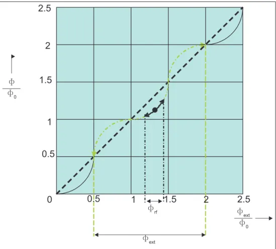
rf-SQUID in Hysteretic mode (Dispersive Mode): For the case β0 L> 1,
the unstable nature of the ΦT vs. Φ curve in Figure 1.9(a) causes the SQUID to
make transitions between stable quantum states as Φ is changed [Fig. 1.9(b)]. For example, when Φ is increased from 0, there is a transition from the k = 0 flux state to the k = 1 state at a critical flux (neglecting fluctuations) Φc= LI0.
(a) (b)
Figure 1.9: The rf-SQUID: (a) Normalized total flux ΦT/Φ0vs normalized applied
flux Φ/Φ0 for different βL0 values. (b) Total flux ΦT vs. applied flux Φ for
rf-SQUID with LI0/Φ0 = 5/4, showing transitions between quantum states in
absence of thermal noise as Φ is increased and subsequently decreased.
peak voltage VT across the resonant circuit increases linearly with Irf until, for
Φ = 0, Irf = Φc/MQ, at which value
VT(0) = ωrfLTΦc/M, (1.30)
where M = κ(LLT)1/2. At this point [A in Figure 1.10] the SQUID makes a
transition to the k = +1 or −1 state. As the SQUID traverses the hysteresis loop, energy ∆E is extracted from the tank circuit. Because of this loss, the peak flux on the next half cycle is less than Φc, and no transition occurs. The tank circuit
takes many cycles to recover sufficient energy to induce a further transition, which may be into either the k = +1 or −1 state. If we now increase Irf, transitions
are induced at the same values of IT and VT but, because energy is supplied at
a higher rate, the stored energy builds up more rapidly after each energy loss ∆E, and transitions occur more frequently. At B, a transition is induced on each positive and negative rf peak, and a further increase in Irf produces the “riser”
BC. At C, transitions from the k = ±1 states to the k = ±2 states occur, and a second step begins. A plot of the peak values VT(0) vs Irf produces the “steps
hysteresis loops in Figure 1.9(b) are shifted by this amount, and one finds
VT±1/2= ωrfLT (Φc− Φ0/2) /M. (1.31)
Figure 1.10: Peak rf voltage, VT, across tank circuit vs. peak rf current, Irf, in
absence of thermal noise for Φ = 0 (solid line) and Φ = ±Φ0/2 (dashed line).
As Irf is increased, this voltage remains constant until the point Φ, at which
the SQUID traverses the hysteresis loop corresponding to the k = 0 → k = +1 transitions once per rf cycle. A further increase in Irf produces the riser FG; at
G, corresponding to a peak rf flux - (Φc+ Φ0/2), transitions k = 0 → k = −1
begin. Thus an applied flux other than nΦ0 (n is an integer) causes the step AB
to split as shown in Figure 1.10.
The model outlined above enables us to calculate the transfer function at values of Irf that maintain the SQUID biased on a step: the change in VT as we
increase Φ from 0 to Φ0/2 is VT(0) − V
(±1/2)
T = ωrfLTΦ0/2M, so that for small
changes in flux in the range 0 < Φ < Φ0/2 we find VΦ = ωrfLT/M. At first sight,
this result seems to imply that VΦ can be increased indefinitely by reducing κ.
This is not the case, since one must ensure that the point F in Figure 1.10 lies to the right of E, that is, DF must exceed DE. To calculate DF we note that the power dissipated in the SQUID is zero at D and approximately I0Φ0ωrf/2π at F,
since the energy dissipated per rf cycle is approximately I0Φ0 for a device with
LI0 ≈ Φ0. Thus, taking account of the fact that the rf currents and voltages are
peak values, we find (Irf(F )− Irf(D)) = VT(±1/2)/2 ≈ I0Φ0ωrf/2π. Furthermore, we
can easily see that Irf(E)− Irf(D) = Φ0/2MQ. Assuming LI0 ≈ Φ0 and using Eq.
1.31, we can write the requirement that DF exceeds DE in the form κ2Q ≥ π/4.
Taking κ ≈ 1/Q1/2, we find that the expression for V
Φ becomes
V Φ ≈ ωrf(QLT/L)1/2 ≈ ωrf(LT/L)1/2/κ. (1.32)
We note that ΦF scales with ωrf and as L−1/2. Detailed theories have been
developed for noise in the hysteretic rf-SQUID operating at liquid Helium temper-atures (Kurkij¨arvi, 1972, 1973; Jackel and Buhrman, 1975; Giffard et al., 1976; Ehnholm, 1977; Hollenhorst and Giffard, 1980; Ryh¨anen et al., 1989). Although in a noise-free model the steps are flat, thermal noise causes them to tilt to a slope η. In addition, thermal noise induces voltage noise on the step arising from fluctuations in the value of flux, at which transitions between flux states occur. The corresponding intrinsic flux noise of the SQUID is (Kurkij¨a rvi, 1973).
Si Φ(f ) ≈ (LI0)2 ωrf à 2πkBT I0Φ0 !4/3 . (1.33)
In the case of Helium-cooled rf-SQUIDs, in which the tank circuit voltage is detected with a room-temperature amplifier, there is a second, extrinsic contri-bution to the flux noise. This arises in part because the noise temperature of the rf amplifier is above the bath temperature and in part because a fraction of the coaxial line connecting the tank circuit to the amplifier is at room temperature. We can represent these two contributions by an effective noise temperature Tef f
a ,
enabling us to write the noise energy due to intrinsic and extrinsic noise sources as (Jackel and Buhrman, 1975; Giffard et al.,1976);
ε ≈ LI 2 0 2ωrf à 2πkBT I0Φ0 !4/3 +2πηkBT ef f a ωrf . (1.34)
Equation 1.34 makes two important points. First, scales as 1/ωrf, up to
a limiting value R/L. Second, for low-Tc SQUIDs, the extrinsic noise energy
generally dominates the intrinsic noise: if we take the representative values T= 4 K, Γ = 0.1, η = 0.2, β0
L = 2π, and Taef f = 100K, we find that the extrinsic
noise energy is about 20 times the intrinsic value. Thus, although we should be wary of extrapolating these results to 77 K, where to our knowledge, there are no simulations or calculations, the overall noise energy of the hysteretic rf-SQUID should not increase very much as we raise the temperature from 4 K to 77 K. This result is in contrast to the dc-SQUID, which for properly designed circuitry is limited largely by intrinsic noise at 4.2 K, so that the overall noise energy will increase significantly as the temperature is raised to 77 K.
rf-SQUID in Nonhysteretic mode (Dissipative mode): To give an ap-proximate account of the operation of the nonhysteretic rf-SQUID, we follow the description of Hansma (1973), which is valid in the limits β0
L ¿ 1, where the
total magnetic flux threading the SQUID is nearly equal to the applied flux, and
ωrf ¿ I0R/Φ0. More general treatments are given, for example, by Jackel and
Buhrman (1975), Erne et al. (1976), Danilov et al. (1980), Likharev (1986), and Ryh¨anen et al. (1989).
In the presence of a static flux Φ and rf flux Φrf sinωrf t, the current in the
SQUID loop is
I = I0sin [(2π/Φ0) (Φ + Φrfsin ωrft)]
(2πLI0 ¿ Φ0).
(1.35)
The oscillating component of this current induces a current Ii = −(M/Z)dI/dt
into the tank circuit, where Z = RT + i[ωrf(LT − M2/L) − 1/ωrfCT] is its
impedance; the inductance of the tank circuit is modified by the contribution
−M2/L from the SQUID. If we assume that the rf frequency is near resonance
and that Q is reasonably large, we can neglect all frequency components other than the fundamental. Expanding the right-hand side of Eq. 1.35 in terms of the Bessel function J1, we find the induced current as,
Ii = 2κ2QLI 0 M(1 + δ2)1/2 cos µ2πΦ rf Φ0 ¶ J1 µ2πΦ rf Φ0 ¶ sin(ωrft − θ). (1.36)
Here, δ = 2[(ωrf − ω0)/ω0]Q is the normalized difference between the rf
fre-quency and the tank-circuit resonant frefre-quency Φ0 , and θ = tan−1δ + π/2.
Figure 1.11: Tank circuit voltage, VT, vs rf drive current IT for four values of the
tuning parameter δ = [2(ωrf− ω0)/ω0]Q and for Φ = 0, andΦ0/2. Curves plotted
for κ2Qβ0
L= π/2 (Hansma, 1973).)
The rf flux applied to the SQUID is MITsinωrft, where IT is the amplitude of
the total current in the inductor, which in addition to the induced current given by Eq. 1.36, also contains a component of amplitude QIrf/(1 + δ2)1/2 produced
by the external rf current. From Eq. 1.36 we see that the total current leads the induced current by a phase angle θ. The amplitudes of the total and external rf currents are related by
Irf = (1 + δ2)1/2 Q " 2κ2QLI 0 (1 + δ2)1/2M cos µ2πΦ Φ0 ¶ × J1 µ2πM I T Φ0 ¶ + IT cos θ #2 + IT2sin2θ 1/2 . (1.37) Figure 1.11 shows plots of VT vs Irf for Φ = 0 and Φ0/2 for four values of
the tuning parameter δ. We see that the response is insensitive to the flux in the SQUID for δ = 0; thus the tank circuit for the nonhysteretic SQUID is operated
off resonance. For a given value of δ, the response shows a series of oscillations as
Irf is increased, arising from the oscillations of the Bessel function. The maximum
peak-to-peak modulation of VT at fixed Irf is of the order of 2κ2QLI0(ωrfLT/M),
so that,
VΦ ≈ (2/π) κ2QβL0ωrfLT/M
≈ (2/π) (κ2Qβ0
L)ωrf(LT/L)1/2/κ.
(1.38)
This transfer function exceeds that of the hysteretic rf-SQUID [Eq. 1.38] by a factor of order κ2Qβ0
L , which can be made larger than unity for the nonhysteretic
case by choosing κ2Q À 1.
The intrinsic noise energy of low-Tc nonhysteretic rf-SQUIDs has been
calcu-lated by several authors, and is approximately 3kBT /(βL0)2ωc (Likharev, 1986),
where the drive frequency is set equal to ωc = R/L, the cutoff frequency of the
SQUID. A noise energy as low as 20¯h has been achieved by Kuzmin et al. (1985). As a preamble to the discussion of nonhysteretic high-TcSQUIDs, we note that
Falco and Parker (1975) successfully observed flux modulation in an rf-SQUID at 2K with a supercurrent as low as 50 nA. The corresponding value of the noise parameter Γ = 2πkBT /I0Φ0 was about 1.7; at this high value, they were unable
to observe any trace of supercurrent in an isolated junction. Thus it is evident that one can expect to operate an rf-SQUID with substantially higher values of Γ than is the case for the dc-SQUID (see Sec. II.C). Although this important fact has been known experimentally for many years, only very recently has the work of Chesca (1998) provided a quantitative explanation. In contrast to previous theories of the rf-SQUID in which one regards thermal noise as a perturbation on a noise-free system, Chesca solves the Smoluchowski equation for the situation, in which thermal fluctuations dominate. Thus both the signal produced by the SQUID and the noise are found in a unified calculation that yields analytical results. For the case β0
L ≤ 1 and ωrf ¿ R/L, Chesca finds;
ε ≈ 3Γ2 Ã 1 + Tk T 1 κ2Q R/L ωrf ! exp(L/L0 th) L/L0 th kBT L0th R . (1.39)
![Figure 3.3: SEJ structure and the asymmetric grain boundary junctions shown for a rf-SQUID magnetometer.[2]](https://thumb-eu.123doks.com/thumbv2/9libnet/5745644.115806/103.892.312.651.176.729/figure-structure-asymmetric-grain-boundary-junctions-squid-magnetometer.webp)
![Figure 3.5: Asymmetric rf-SQUID layout design of tri-junction gradiometer. [3]](https://thumb-eu.123doks.com/thumbv2/9libnet/5745644.115806/106.892.257.705.349.755/figure-asymmetric-squid-layout-design-tri-junction-gradiometer.webp)
![Figure 3.6: Asymmetric rf-SQUID layout design of bi-junction magnetometer.[3]](https://thumb-eu.123doks.com/thumbv2/9libnet/5745644.115806/107.892.258.706.297.684/figure-asymmetric-rf-squid-layout-design-junction-magnetometer.webp)