HIGHLY-DOPED SILICON BASED
PHOTONIC DEVICES FOR MID-INFRARED
LIGHT ABSORPTION
a thesis submitted to
the graduate school of engineering and science
of bilkent university
in partial fulfillment of the requirements for
the degree of
master of science
in
electrical and electronics engineering
By
Kazim G¨
org¨
ul¨
u
July 2017
HIGHLY-DOPED SILICON BASED PHOTONIC DEVICES FOR MID-INFRARED LIGHT ABSORPTION
By Kazim G¨org¨ul¨u July 2017
We certify that we have read this thesis and that in our opinion it is fully adequate, in scope and in quality, as a thesis for the degree of Master of Science.
Ekmel ¨Ozbay(Advisor)
Bayram B¨ut¨un(Co-Advisor)
Ayhan Altınta¸s
Sefer Bora Li¸sesivdin Approved for the Graduate School of Engineering and Science:
Ezhan Kara¸san
ABSTRACT
HIGHLY-DOPED SILICON BASED PHOTONIC
DEVICES FOR MID-INFRARED LIGHT ABSORPTION
Kazim G¨org¨ul¨u
M.S. in Electrical and Electronics Engineering Advisor: Ekmel ¨Ozbay, Co-Advisor: Bayram B¨ut¨un
July 2017
Electromagnetic wave absorbers have the potential to enable important applica-tions in the mid-infrared wavelength range such as thermal imaging and infrared spectroscopy. The choice of absorbing material has significant implications for the ultimate utility of any photonic device or structure. So far, traditional metals are employed as common absorbing materials, especially in metamaterial designs. However, many of these metals react with the atmosphere or water, limiting their utility for a wide range of applications. There are many materials, other than conventional metallic components, that exhibit lossy properties and pro-vide advantages in device performance, design exibility, fabrication, integration, and tunability. Here, we investigate highly doped silicon as an efficient absorb-ing material for the mid-infrared regime. The absorption is achieved by the free carriers in the silicon which can be spectrally tuned by controlling its carrier concentration.
Most of the resonant absorbers suffer from narrow operating absorption wave-band. A common approach is to use multiple resonance centers to increase band-width. However, the number of resonators combined within the same unit cell is limited. We propose highly doped silicon based absorbers with a patterned silicon-on-insulator substrate that provide enhanced bandwidth without compro-mising absorption performance. Broadband absorption is achieved by the com-bined effects of bulk absorption, and vibrational and plasmonic absorption reso-nances. Moreover, we investigate black silicon concept for mid-infrared regime. The structures investigated unveil wideband and efficient absorbers. An ana-lytical description of the wave propagation in black silicon texture is presented, showing agreement with the experiment and the computational analysis.
iv
bio-chemical and refractive index sensors, require narrow absorption bands. Plas-monic absorbers typically have narrow resonance bands and they can be utilized in highly sensitive detection schemes. Traditional metals are common materials for these applications. However, apart from their fabrication challenges, they have extremely large, negative permittivity. This feature of metals significantly limits their plasmonic mode confinement in the mid-infrared regime. In this regime, highly doped silicon is a promising plasmonic material for sensing applications owing to its suitable plasma frequency. Here, we demonstrate plasmonic per-fect absorbers based on high conductivity silicon and investigate refractive index sensing performance of the absorbers.
Keywords: silicon, mid-infrared, absorber, plasmonics, black silicon, refractive index sensing.
¨
OZET
Y ¨
UKSEK DERECEDE DOPLANMIS
¸ S˙IL˙IKON
TABANLI FOTON˙IK YAPILAR ˙ILE ORTA-KIZIL ¨
OTES˙I
IS
¸I ˘
GIN EM˙IL˙IM˙I
Kazim G¨org¨ul¨u
Elektrik ve Elektronik M¨uhendisli˘gi, Y¨uksek Lisans Tez Danı¸smanı: Ekmel ¨Ozbay, E¸s Danı¸sman: Bayram B¨ut¨un
Temmuz 2017
Elektromanyetik dalga so˘gurucuları orta-kızıl¨otesi b¨olgede termal g¨or¨unt¨uleme ve kızıl¨otesi spektroskopi gibi ¨onemli uygulamalara imkan sa˘glamaktadırlar. So˘gurucu materyalin se¸cimi herhangi bir fotonik yapının kullanı¸slılı˘gında ¸cok ¨
onemli bir etkiye sahiptir. Bu zamana kadar, ¨ozellikle de metamalzemeli yapılarda, geleneksel metaller so˘gurucu materyal olarak kullanılmı¸slardır. Fakat, bu metallerin bir ¸co˘gu atmosferle veya su ile tepkimeye girmekte ve bu da on-ların bir¸cok uygulamada kullanımını sınırlandırmaktadır. Bu metallerin dı¸sında so˘gurucu ¨ozelliklere sahip bir¸cok materyal bulunmakta ve bu materyaller perfor-mans, tasarım esnekli˘gi, ¨uretim, entegrasyon ve tonlanabilirlik a¸cısından avantaj sa˘glamaktadır. Biz burada, y¨uksek d¨uzeyde doplanmı¸s silikonu orta-kızıl¨otesi b¨olgede so˘gurucu bir materyal olarak inceledik. So˘gurma, silikon i¸cerisindeki serbest ta¸sıyıcılar ile sa˘glanmakta ve silikonun i¸cerisindeki ta¸sıyıcı yo˘gunlu˘gu de˘gi¸stirilerek kontrol edilebilmektedir.
Rezonant so˘gurucuların ¸co˘gu dar i¸sletim dalgabandına sahiptir. C¸ oklu re-zonans merkezlerinin aynı anda kullanılması band geni¸sli˘gini artırmanın yaygın y¨ontemidir. Ancak, aynı birim yapıdaki rezonat¨or sayısı sınırlıdır. Biz burada so˘gurma veriminden taviz vermeden y¨uksek derecede doplanmı¸s silikon tabanlı, ¸sekillendirilmi¸s yalıtkan ¨uzerinde silikon altta¸s kullanarak, ultra geni¸s bantlı bir so˘gurucu ¨onerdik. Geni¸s bantlı so˘gurma ¨ozelli˘gi k¨utle (bulk) so˘gurma, vibrasyonel ve plazmonik so˘gurmanın birle¸siminden gelmektedir. Biz ayrıca bu ¸calı¸smaya ek olarak siyah silikon kavramını orta-kızıl¨otesi ı¸sık i¸cin inceledik. Bu yapılar ile de geni¸s bantlı ve y¨uksek performanslı so˘gurucular elde ettik. Elektromanyetik dal-ganın bu yapı ile etkile¸simini analitik olarak a¸cıkladık ve deneysel ve simulasyon sonu¸cları ile kar¸sıla¸stırdık.
vi
Biyo-kimyasal ve kırılma endeksi sens¨orleri ile se¸cici termal yayıcılar ve dedekt¨orler gibi bazı uygulamalar ise dar bir so˘gurma bandı gerektirirler. Plaz-monik so˘gurucular genelde dar so˘gurma bandına sahiptirler ve bu y¨uzden y¨uksek derecede hassas algılama d¨uzeneklerinde kullanılabilirler. Bu uygulamalarda ge-leneksel metaller yaygın olarak kullanılırlar. Fakat, ¨uretimdeki zorluklarının yanında metaller orta-kızıl¨otesi b¨olgede ¸cok negatif bir elektriksel ge¸cirgenli˘ge sahiptir bu y¨uzden metallerin plazmonik mod toplanması zorla¸smaktadır. Bu b¨olgede y¨uksek derecede doplanmı¸s silikon, uygun plazma frekansından dolayı, gelecek vaad eden bir materyaldir. Biz burada y¨uksek derecede doplanmı¸s si-likon kullanarak y¨uksek verimlilikte bir plazmonik so˘gurucu tasarladık ve bu so˘gurucuyu kırılma endeksi sens¨or¨u olarak inceledik.
Anahtar s¨ozc¨ukler : silisyum, orta-kızıl¨otesi, so˘gurucu, plazmonik, siyah silisyum, kırılma endeks sens¨or¨u.
Acknowledgement
I would like to thank my former advisor Prof. Ali K. Okyay for his guidance in the first year of my master’s degree studies. I also thank my current advisor and co-advisor Prof. Ekmel ¨Ozbay and Dr. Bayram B¨ut¨un for their guidance in the second year of my master’s degree studies.
I would like to thank Prof. Ayhan Altınta¸s and Prof. S. Bora Li¸sesivdin for being members of my thesis committee and their valuable comments.
I am grateful to Dr. Mehmet Yılmaz and Dr. Ka˘gan Topallı for their help and support. I would like to thank Abdullah G¨ok for his help and guidance in my studies. I thank Sami Bolat for his devoted help in my lab works. I also thank Z¨ulkarneyn and Sina for their help and for being nice friends to me.
Contents
1 Introduction 1
1.1 Background and Motivation . . . 1 1.2 Thesis Overview . . . 3
2 Theory and methods 5
2.1 Surface plasmons . . . 5 2.1.1 Wave Equation . . . 5 2.1.2 Surface plasmon polaritons at a dielectric-metal interface . 8 2.1.3 Surface plasmon polaritons at multilayer systems . . . 10 2.2 Finite-difference time-domain method . . . 13 2.3 Optical characterization of highly doped silicon . . . 15
3 Ultra-Broadband infrared light absorption with patterned silicon-on-insulator (SOI) substrate 18 3.1 Introduction . . . 18
CONTENTS ix
3.2 Methods . . . 20
3.2.1 Device fabrication and measurement . . . 20
3.2.2 Simulations . . . 21
3.3 Results and discussions . . . 22
3.4 Conclusion . . . 31
4 Silicon based plasmonic surfaces for sensing 32 4.1 Introduction . . . 32
4.2 Structure and methods . . . 34
4.3 Results and discussions . . . 36
4.4 Conclusion . . . 41
5 Fabrication and optical modeling of black silicon for mid-infrared light applications 42 5.1 Introduction . . . 42
5.2 Structure and methods . . . 44
5.3 Results and discussions . . . 47
5.4 Conclusion . . . 49
List of Figures
2.1 Geometry for surface plasmon polaritons at a dielectric-metal in-terface . . . 8 2.2 Geometry for surface plasmon polaritons at three-layer system . . 11 2.3 (a)Real and imaginary parts of the permittivity for heavily doped
n-type and p-type silicon for top and bottom silicon layers of our structure.(b)Measured, simulated and analytically calculated (T-matrix) reflection spectrum of the SOI structure. Inset illustrates the SOI structure. . . 15 2.4 (a) Optical constants of a plain silicon wafer with a carrier
con-centration of 7 × 10¹⁹ fitted with spectroscopic ellipsometry. . . . 17 3.1 (a) Process flow for fabrication of silicon based 2D gratings
utiliz-ing SOI structure. First, 2.0 µm thick Si is thinned down to 1.2 µm Si. For simplicity, this step is not shown in the figure. Af-ter thinning the device Si layer, the rest of the patAf-terning steps are explained in this illustration. (a) Spin coating of photoresist, (b) photolithography patterning, (c) etching of silicon by BOSCH process, (d) removal of photoresist with oxygen plasma. . . 21
LIST OF FIGURES xi
3.2 (a) Schematic representation of a three layer silicon-silicon dioxide-silicon structure with the top dioxide-silicon layer patterned as 2D gratings of periodicity P, (b) SEM image of one of the fabricated samples with periodicity, P=8 µm. Scale bar is 4 µm. . . 22 3.3 (a,b) Simulated reflection (Sim. Ref.), transmission (Sim. Trans.)
and absorption (Sim. Abs.) spectra and measured reflection (Exp. Ref.) spectrum for the samples with periodicities of P=7 µm and P=8 µm. . . 24 3.4 (a) Simulated absorption spectra of the 1D structure with
period-icity 8 µm and fill ratio of 0.5 for TE and TM polarizations. Inset shows the schematic of 1D silicon silicon dioxide silicon structure (b) Calculated spatial field distributions for the same structure with periodicity of 8 µm at λ=7 µm, λ=12 µm, λ=15 µm, and λ=18 µm. The arrows represent the electric field vector. . . 25 3.5 Simulated absorption spectra of 4 µm thick silicon with different
doping concentrations. . . 26 3.6 (a) Simulated and analytical dispersion relation for the
silicon-silicon dioxide-silicon-silicon-air structure. Abbr: BPs (Bulk Plasmons), PSPs (Propagating Surface Plasmons), GPs (Gap Plasmons). (b) Dependence of the absorption spectrum on the structure periodic-ity. Fill ratio is kept constant as 0.5 and the periodicity is varied from 6 µm to 9 µm. . . 27 3.7 (a) Absorption spectrum as a function of wavelength and doping
density. (b) Absorption spectrum of the structure with periodicity 8 µm and fill ratio 0.5 for three different incidence angles. The structure is illuminated by a TM polarized plane wave. (c) Average absorption as a function of angle of incidence for TM and TE polarizations. (d) Absorption spectrum as a function of wavelength and angle of incidence. . . 30
LIST OF FIGURES xii
4.1 (a) Schematic illustration of 2D grating structures. (b) Top-view scanning electron microscope image of the 2D plasmonic absorber structure with periodicity of P = 8 µm and fill ratio of 0.65. Scale bar is 10 µm. (c) Measured and simulated reflection from the flat silicon surface. . . 35 4.2 (a) Simulated and measured reflection spectra for structures with
periodicities of P = 8 µm and P = 9 µm, and fill ratio of 0.65 for both structures. (b) Cross section of the time-averaged magnetic field for the structure with periodicity P = 9 µm at the resonance wavelength. (c) Cross section of the time-averaged optical power flow vector distribution. . . 37 4.3 Simulated and measured reflection spectra at three different
inci-dence angles for the structure with P = 12 µm, fill ratio of 0.45 and height of 1.4 µm. The inset shows the fabricated 1D device structure. . . 38 4.4 (a) Measured reflection spectra of the structure with periodicity
P = 9 µm in two different media. Red arrows show the molecu-lar resonance points of the acetone. Blue arrows show the plas-monic resonances of the patterned silicon under air and acetone. (b) Simulated reflection spectra for different refractive indices of the surrounding medium. (c) Measured and simulated resonance wavelengths as a function of refractive index of the surrounding medium. . . 40 4.5 Reflection spectrum as a function of doping density for the
struc-ture with periodicity P = 9 µm and fill ratio of 0.65. (b) Calculated sensitivity and FOM as a function of doping density. . . 41
LIST OF FIGURES xiii
5.1 (a) SEM images of one of the fabricated samples. Scale bars are 1 µm (b) implementation of black silicon structure into the simu-lation environment. (c) Structural approximation of black silicon, effective medium theory (EMT) for this structure, and transfer matrix formalism (TMF). . . 45 5.2 Simulated and analytically calculated reflection spectra of highly
doped silicon with 7.5 × 10¹⁹ doping concentration, fill ratio 0-0.6.
Analytical calculations conducted for different approximation levels. 47 5.3 (a) Simulated and analytical reflection spectra of flat and black
silicon for three different doping concentrations. (b) Simulated absorption spectra of flat silicon and black silicon with thickness of 4 µm for three different doping concentrations. . . 51 5.4 Experimental, simulated and analytical reflection spectra for the
Chapter 1
Introduction
1.1
Background and Motivation
Electromagnetic (EM) wave absorbers absorbs incident radiation at the frequency of operation by suppressing reflection, transmission and scattering in the struc-ture. EM wave absorbers are of great importance due to their potential in various applications. These applications briefly include: emitters, sensors, anti-reflective coatings, spatial light modulators, photovoltaics etc.
Considerable recent research has focused on increasing the efficiency of energy absorption processes. Highly efficient light absorption with structures consist of single layer or multiple layers of lossy materials [1–3]. Metamaterial absorbers are also widely explored as promising candidates to enhance EM wave absorption at microwave, terahertz, infrared, and visible frequencies [4–8]. However, confined by resonance nature of the unit structures, these metamaterial absorbers generally absorb light within a narrow wavelength range. Researchers tried to increase the absorption waveband by exploiting multiple resonances simultaneously, for applications where broadband absorption is desirable.
Some applications, such as selective thermal emitters and detectors, and bio-chemical and refractive index sensors, require narrow absorption bands [9, 10]. Plasmonic absorbers typically have narrow resonance bands and therefore they can be utilized in spectrally selective detection schemes such as uncooled mi-crobolometers [4]. Narrow resonance bands are highly desirable in sensing ap-plications in order to detect minute changes in the environment. Plasmonic res-onances, confined to a metal dielectric surface, are extremely sensitive to the refractive index of the surrounding dielectric medium. Such strong dependency on the refractive index of the surrounding dielectric medium paves the way for ultra-sensitive label-free refractive index sensing applications [11, 12].
All examples mentioned above utilize conventional metallic components, such as gold and silver, as their material building blocks. In commonly used metals, the magnitude of the real part of the permittivity is very large at mid-infrared wavelengths. This feature of metals significantly limits their plasmonic mode confinement in the mid-infrared regime [13]. Moreover, the devices made of con-ventional metals are not compatible with CMOS processes (such as Au) and that have degradation problem upon exposure to air and humidity such as Ag. Alternatively, there are many materials, other than conventional metals, that provide advantages in device performance, integration, and tunability such as semiconductors, transparent conducting oxides, metal nitrides, perovskite oxides, silicides, germanides, and 2D materials [13, 14]. Among these materials, semi-conductors have attracted great interest due to their well-established fabrication and integration technology. To date, various plasmonic and metamaterial ab-sorbers have been studied with different semiconductors including ZnO, InAs, InSb, Ge [13,15,16]. Demonstration of plasmonic effects by silicon in the infrared region is carried out by others [17,18]. Excitation of plasmonic resonances on sili-con surface is very important for CMOS compatible devices in the infrared region. In addition to silicon plasmonics, needle-like black silicon structures emerged as interesting material with broadband absorbance of more than 99%. So far black silicon structures are presented in the visible and the near-infrared region mostly for photovoltaic and surface enhanced sensing applications. Doping of silicon can bring black silicon concept to the mid-infrared range.
In this thesis, we investigate highly-doped silicon as a material for obtaining highly efficient and ultra-wideband absorbers operating in the mid-infrared re-gion. We also study the refractive index sensing performance of highly-doped silicon based perfect absorbers.
1.2
Thesis Overview
In this first chapter, we introduce conventional absorbers. We emphasize plas-monic and metamaterial absorbers made by conventional metals. Then, we dis-cuss about alternative absorber materials and their advantages over conventional metals and we present highly doped silicon as a material for absorber in the mid-infrared range.
In Chapter 2, we present theoretical background and methods. Plasmonic ab-sorption is one of the main abab-sorption mechanism for the proposed structures in this thesis. Therefore, we investigate surface plasmon polaritons at a single in-terface and multilayer systems. Numerical calculations based on finite difference time domain method are also frequently used. Therefore, we describe the simu-lation method. Then we give Drude model and extraction of optical constants of highly doped silicon via ellipsometric measurements in this chapter.
In chapter 3, we give detailed background on the previous works related with wideband absorbers operating in the mid-infrared regime. We present design and fabrication of the structure. Then, we provide simulation and experimental results, and discuss about absorption mechanisms. Then, we talk about the de-pendence of the absorption spectrum on the doping density of silicon and angular dependence of the absorption spectrum.
In Chapter 4, a detailed background on the previous works related with plas-monic perfect absorbers used for refractive index sensing is given. Then, usage of silicon for refractive index sensing operating in the mid-infrared range is em-phasized. Design and fabrication of the structure is discussed. Simulation and
experimental results for the perfect absorbers with different periodicity for normal and oblique incidences is presented. Then refractive index sensing experiment is provided. Finally, the dependence of sensing performance of the structure on the doping concentration of silicon is discussed.
Chapter 5 is about moving the black silicon concept from visible to the infrared region. A detailed background on the previous works related with black silicon concept is given. Then fabrication of black silicon pattern and implementing this pattern in the simulation environment is described. Then, an analytical description of the wave propagation in black silicon texture is given. Comparison of the experimental, simulated and analytical reflection results is presented.
Chapter 2
Theory and methods
2.1
Surface plasmons
2.1.1
Wave Equation
We will start by reviewing Maxwell’s equations. The relation between four macro-scopic fields ~D (the dielectric displacement or electric flux density), ~E (the electric field), ~H (the magnetic field), and ~B (the magnetic induction or magnetic flux density) in differential form is:
∇ · ~D = ρext (2.1) ∇ · ~B = 0 (2.2) ∇ × ~E = −µ0∂ ~H ∂t (2.3) ∇ × ~H = ~Jext+ ∂ ~D ∂t (2.4)
The flux density vectors can also be expressed as: ~
D = ε0E + ~~ P (2.5)
~
B = µ0H + µ~ 0M~ (2.6)
where ε0 and µ0 are the permittivity and permeability of vacuum, respectively.
~
P is polarization density and ~M is magnetization density. We will only deal with nonmagnetic media, we do not need to consider magnetization. In a linear, isotropic and homogeneous medium electric polarization can be expressed as:
~
P = ε0χ ~E (2.7)
Then flux density vectors become: ~
D = ε0ε ~E (2.8)
~
B = µ0µ ~H (2.9)
where ε = 1 + χ is the dielectric constant or relative permittivity and µ = 1 relative permeability of the nonmagnetic medium.
The wave equation can be obtained for a source free medium by first applying a curl on eq. 2.3 and substituting eq 2.4 into 2.3.
∇ × ∇ × ~E = −µ0∂
2D~
∂t2 (2.10)
Using the vector identity, ∇ × ∇ × ~E ≡ ∇(∇ · ~E) − ∇2E and due to source~ free medium ∇ · ~D = 0 wave equation becomes:
∇2E −~ µ0ε0ε∂2E~
∂t2 = 0 (2.11)
Assuming harmonic time dependence, E(r, t) = E(r)e~ −jωt equation 2.11 be-comes:
∇2E + k~ 02ε ~E = 0 (2.12)
where k0 = ω
√
µ0ε0 = ωc is the wave vector of the wave in free space.
For harmonic time dependence we arrive following six coupled equations:
∂Ez ∂y − ∂Ey ∂z = jωµ0Hx (2.13) ∂Ex ∂z − ∂Ez ∂x = jωµ0Hy (2.14) ∂Ey ∂x − ∂Ex ∂y = jωµ0Hz (2.15) ∂Hz ∂y − ∂Hy ∂z = −jωε0εEx (2.16) ∂Hx ∂z − ∂Hz ∂x = −jωε0εEy (2.17) ∂Hy ∂x − ∂Hx ∂y = −jωε0εEz (2.18) For propagation in the x-direction and homogeneity in the y-direction
∂Ey ∂z = −jωµ0Hx (2.19) ∂Ex ∂z − jβEz = jωµ0Hy (2.20) jβEy = jωµ0Hz (2.21) ∂Hy ∂z = jωε0εEx (2.22) ∂Hx ∂z − jβHz = −jωε0εEy (2.23) jβHy = −jωε0εEz (2.24)
Combining 2.20, 2.22 and 2.24 one can achieve wave equation of Hy for
∂2H y
∂z2 + (k0 2
ε − β2)Hy = 0 (2.25)
Combining 2.19, 2.21 and 2.23 one can achieve wave equation of Ey for
Trans-verse Electric (TE) polarization.
∂2E y
∂z2 + (k0
2ε − β2)E
y = 0 (2.26)
2.1.2
Surface plasmon polaritons at a dielectric-metal
in-terface
Figure 2.1 depicts the simple geometry that can support surface plasmon polari-tons at single interface. The solution for surface plasmon propagates along the interface and decays exponentially in the z-direction.
Figure 2.1: Geometry for surface plasmon polaritons at a dielectric-metal inter-face
for z > 0 Hy(z) = A1ejβxe−k1z (2.27) Ex(z) = jA1ejβxe−k1zk1 ωε1ε0 (2.28) Ez(z) = −A1βejβxe−k1z ωε1ε0 (2.29) for z < 0 Hy(z) = A2ejβxek2z (2.30) Ex(z) = −jA2ejβxek2zk2 ωε2ε0 (2.31) Ez(z) = −A2βejβxek2z ωε2ε0 (2.32)
Continuity of the tangential components along the interface gives A1 = A2
and, k2 k1 = − ε2 ε1 (2.33)
This requires that permittivities of region 1 and 2 should have opposite signs that means surface plasmons can exist at interfaces between materials with oppo-site signs such as metals and insulators. The solution for Hy should also satisfy
the wave equation:
k12 = β2− k02ε1 (2.34)
k22 = β2− k02ε2 (2.35)
combining 2.33 2.34 and 2.35 we can obtain dispersion relation at a dielectric metal interface:
β = k0 r ε1ε2 ε1+ ε2 (2.36) For TE solutions: for z > 0 Ey(z) = A1ejβxe−k1z (2.37) Hx(z) = −jA1ejβxe−k1zk1 ωµ0 (2.38) Hz(z) = A1βejβxe−k1z ωµ0 (2.39) for z < 0 Ey(z) = A2ejβxek2z (2.40) Hx(z) = jA2ejβxek2zk2 ωµ0 (2.41) Hz(z) = A2βejβxek2z ωµ0 (2.42)
Continuity of tangential components along the interface gives:
A1(k1+ k2) = 0 (2.43)
Since k1 > 0 and k2 > 0 this condition is satisfied when A1 = A2 = 0.
Therefore surface plasmons are not supported for TE polarization.
2.1.3
Surface plasmon polaritons at multilayer systems
In this section we will investigate surface plasmon dispersion relation at multi-layers as shown in Figure 2.2. In this system there are two interfaces separated
from each other. If the separation is comparable to the decay length of surface plasmons, interactions between surface plasmons give rise to coupled modes. For TM polarization:
Figure 2.2: Geometry for surface plasmon polaritons at three-layer system for z > d/2 Hy(z) = A1ejβxe−k1z (2.44) Ex(z) = jA1ejβxe−k1zk1 ωε1ε0 (2.45) Ez(z) = −A1βejβxe−k1z ωε1ε0 (2.46) for z < −d/2 Hy(z) = A3ejβxek3z (2.47) Ex(z) = jA3ejβxek3zk3 ωε3ε0 (2.48) Ez(z) = −A3βejβxek3z ωε3ε0 (2.49)
for −d/2 < z < d/2 Hy(z) = B1ejβxe−k2z+ B2ejβxe−k2z (2.50) Ex(z) = −jB1ejβxek2zk2 ωε2ε0 + jB2e jβxe−k2zk 2 ωε2ε0 (2.51) Ez(z) = B1βejβxek2z ωε2ε0 +−B2βe jβxe−k2z ωε2ε0 (2.52)
Continuity of tangential components along two interfaces gives: at z = d/2 A1e−k1d/2 = B1ek2d/2+ B2e−k2d/2 (2.53) A1k1e−k1d/2 ε1 = −B1k2e k2d/2 ε2 + B2k2e −k2d/2 ε2 (2.54) at z = −d/2 A3e−k3d/2 = B1e−k2d/2+ B2ek2d/2 (2.55) −A3k3e−k3d/2 ε3 = −B1k2e −k2d/2 ε2 + B2k2e k2d/2 ε2 (2.56)
The solution for Hy should also satisfy the wave equation:
k12 = β2− k02ε1 (2.57)
k22 = β2− k02ε2 (2.58)
k32 = β2− k02ε3 (2.59)
Solving equations 2.53 to 2.59 results in an implicit expression for the disper-sion relation of three layer system.
e−2k2d= k2/ε2+ k1/ε1
k2/ε2− k1/ε1
k2/ε2+ k3/ε3
k2/ε2− k3/ε3
(2.60)
2.2
Finite-difference time-domain method
The finite-difference time-domain (FDTD) method is a general, straightforward implementation of Maxwell’s equations in time domain for the solution of a va-riety of electromagnetic wave problems. The FDTD method is formulated by discretization of Maxwell’s equations over a finite volume and and approximating the derivatives with central difference approximation.
Firstly, we will discretize scalar equation of Amperes law which involves partial derivative of electric field intensity(Ex) with respect to time at t = n∆t and
z = k∆z. σExn(k) + ε Exn+1/2(k) − Exn−1/2(k) ∆t = − Hyn(k + 1/2) − Hyn(k − 1/2) ∆z (2.61) For the value of Ex at time step n, we have semi-implicit approximation:
Exn(k) =
Exn+1/2(k) − Exn−1/2(k)
2 (2.62)
By replacing this approximation for the equation above we have:
σEx n+1/2 (k) − Exn−1/2(k) 2 + ε Exn+1/2(k) − Exn−1/2(k) ∆t = − Hyn(k + 1/2) − Hyn(k − 1/2) ∆z (2.63)
(σ 2 + ε ∆t)Ex n+1/2(k) = (−σ 2 + ε ∆t)Ex n−1/2(k) − Hyn(k + 1/2) − Hyn(k − 1/2) ∆z (2.64) Exn+1/2(k) = ( 1 − ∆tσ/2ε 1 + ∆tσ/2ε)Ex n−1/2 (k) − ( 2∆t (∆tσ + 2ε)∆z) Hyn(k + 1/2) − Hyn(k − 1/2) ∆z (2.65)
Secondly, we will discretize scalar equation of Faradays law which involves partial derivative of Hy with respect to time at t = (n +1/2) t and z = (k+1/2)z.
−µHx n+1(k + 1/2) − H xn(k + 1/2) ∆t = Eyn+1/2(k + 1) − Eyn+1/2(k) ∆z (2.66) Hxn+1(k + 1/2) − Hxn(k + 1/2) = −( ∆t µ∆z) Eyn+1/2(k + 1) − Eyn+1/2(k) ∆z (2.67) Hxn+1(k + 1/2) = Hxn(k + 1/2) − ( ∆t µ∆z) Eyn+1/2(k + 1) − Eyn+1/2(k) ∆z (2.68)
These equations (2.65 and 2.68) can be directly implemented in a computer code. Once the spatial resolution ∆z is chosen, the absolute size of the computa-tional domain can be determined. While choosing the resolution it is necessary to have at least 10 cells per wavelength (smallest wavelength in the simulation) for an adequate simulation. Then, we can determine the time step necessary accord-ing to the spatial resolution. Finally, we should implement a cycle to compute the fields for a certain number of time steps.
2.3
Optical characterization of highly doped
sil-icon
In order to determine optical properties of the highly doped silicon, Drude for-malism is used:
ε(ω) = ε∞(1 −
ωp2
ω(ω + jτ)) (2.69) where ε∞ is the permittivity value for ω >> ωp and taken as 11.7, τ is the
relaxation time, ωp is the plasma frequency:
ωp2 =
N e2 ε0ε∞m∗m0
(2.70)
where N is the free carrier concentration per cm3, e is the elementary charge, ε0is the vacuum permittivity, m∗ is the effective mass, and m0 is the electron
mass.
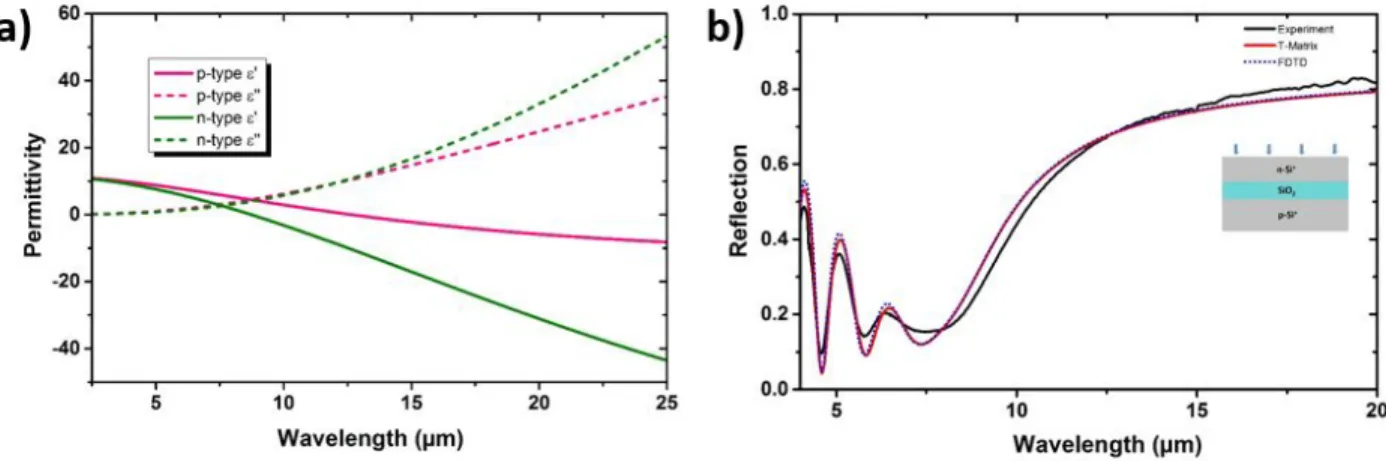
Figure 2.3: (a)Real and imaginary parts of the permittivity for heavily doped n-type and p-type silicon for top and bottom silicon layers of our struc-ture.(b)Measured, simulated and analytically calculated (T-matrix) reflection spectrum of the SOI structure. Inset illustrates the SOI structure.
One of our substrates is a procured SOI wafer has n-type silicon layer at the top and p-type silicon layer at the bottom. Resistivity values of these silicon layers correspond to the doping density on the order of N = 5 × 1019cm−3. In
order to extract optical properties of the both n-type and p-type silicon layers we consider plasma frequency and relaxation time as our fitting parameters and we start calculations with N = 5 × 1019cm−3 and 1/τ = 0.037 (eV) [19]. We optimized these parameters by fitting FDTD calculations to our experimental results. Eventually we obtained best fit for Nn = 5.2 × 1019cm−3. and, Np =
5.5 × 1019cm−3. for n-type and p-type silicon layers, respectively. These carrier
concentration values correspond to plasma wavelengths of λn = 8.28µm and
λp = 9.42µm for n-type and p-type silicon layers, respectively. Figure 2.3a shows
the modeled real and imaginary permittivity values of our n-type and p-type silicon layers. Figure 2.3b shows the measured, simulated and also analytically calculated (T-matrix formalism) reflection results of the SOI structure without patterning. In numerical calculations optical constants of silicon dioxide have taken from the literature [20]. As seen in this figure the numerical and the analytical reflection spectra fit very well to the experimental reflection spectrum indicating validity of our model.
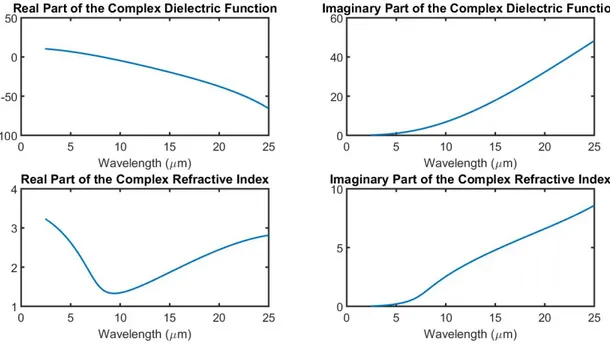
Here we tried to extract optical properties by given approximate resistivity values (or approximate doping densities) and using a normal incidence reflec-tion result. Even if we get a relatively consistent fitting results for this, there is more accurate method for this extraction, ellipsometry. Ellipsometry is a tech-nique that is used to extract the optical constants of a material by measuring the change in the polarization of a light beam reflected from the material. In spectroscopic ellipsometry technique multiple measurements are taken for differ-ent incidence angles to increase accuracy. Figure 2.4 shows optical constants of a plain silicon wafer with a carrier concentration of 7×10¹⁹fitted with spectroscopic ellipsometry.
Figure 2.4: (a) Optical constants of a plain silicon wafer with a carrier concen-tration of 7 × 10¹⁹ fitted with spectroscopic ellipsometry.
Chapter 3
Ultra-Broadband infrared light
absorption with patterned
silicon-on-insulator (SOI)
substrate
This chapter will be based on the publication “All-Silicon Ultra-Broadband In-frared Light Absorbers” K. Gorgulu et al., Scientific Reports, 6, (2016): 38589. Reproduced (or Reproduced in part) with permission from Nature Publishing Group. Copyright 2016 Nature Scientific Reports.
3.1
Introduction
By exploiting plasmonic structures, electromagnetic energy can be localized into a very small volume and efficient conversion between photons and plasmons can be controlled at sub-wavelength scale [21, 22]. Noble metals such as gold and silver are commonly used plasmonic materials at visible (VIS) and near-infrared (NIR) ranges. In order to exploit plasmonic enhancement in the mid-wave and
long-wave infrared regions, materials with plasma frequencies in this range are required. Common metals have plasma frequencies in VIS and NIR regions. On the other hand, plasma frequency of semiconductors can be modulated by either changing charge carrier concentration (doping) or applying potential gat-ing [14, 23]. Therefore, highly doped semiconductors emerge as favorable alterna-tives of metals in plasmonics, especially in the infrared region. The performance of various semiconductor materials has been evaluated in a number of theoreti-cal and experimental studies [24–27]. Among these semiconductors, silicon has attracted great interest due to silicon integrated photonic devices including sub-wavelength interconnects, modulators, and emission sources [23, 28]. Silicon also enables chip scale integration at mid-infrared (MID-IR) band where many po-tential applications arise including chemical and biological sensors, imagers, light sources and spectroscopy [29].
Demonstration of plasmonic effects by silicon in the infrared region is car-ried out by others [17, 18]. Several groups have studied silicon based surface plasmon resonances for bio-chemical sensing applications [30–32]. Frequency selective infrared absorbers have been proposed based on low-resistivity silicon gratings [33, 34]. For spectroscopy and imaging applications, it is highly desir-able to have wideband absorbers. Most of the resonant absorbers suffer from narrow operating absorption waveband. Much of the work in this direction fo-cuses on multi-resonance or tapered metamaterial structures to increase band-width [35–37]. One way of increasing absorption band is to use multilayered structures composed of lossy materials absorbing the light gradually. Recently, two studies were reported as in the form of a geometric transition absorber based on metal-dielectric slabs [36, 37]. Another approach is to combine different res-onators to obtain wideband or multiband response [35, 38, 39]. However, as the number of resonators increases, so does the size of a unit cell, the fill factor and the absorption efficiency decrease. Therefore, highly efficient and ultra-wideband ab-sorbers have not previously been proposed or implemented in the MID-IR region. In this study, we theoretically and experimentally demonstrate an ultra-wideband MID-IR absorber. Furthermore, we show that the absorption is related to the free carrier absorption, and vibrational and plasmonic resonances supported by
the structure simultaneously. The absorber demonstrated in this study has an enhanced bandwidth without compromising absorption performance by allevi-ating the issues encountered in the previous studies presented in the literature. More importantly, proposed absorber is based on silicon and it extends silicon photonics to the mid-infrared wavelengths for optoelectronic systems. Such an absorber paves the way to the realization of all-silicon based sensors, imagers and spectroscopy applications, and provides chip-scale integration compatible with CMOS technology [40].
3.2
Methods
3.2.1
Device fabrication and measurement
Fabrication of our structures starts with commercial SOI wafers consisting of 500 µm thick highly doped handle layer silicon substrate at the bottom with resistivity range of ρ = 0.002 − 0.005Ω − cm, 800 nm thick silicon dioxide in the middle and 2 µm thick highly doped device layer silicon at the top with resistivity range of ρ = 0.001 − 0.0015Ω − cm. We first thinned the device layer silicon from 2 µm to 1.2 µm by using an SF6 based isotropic RIE process. After
thinning the device layer of the SOI to the desired thickness of 1.2 µm, we used standard photolithography procedures to define the desired patterns. First, we spun a positive photoresist (AZ 5214E) at 4000 r.p.m. and baked the photoresist at 110 ◦C for 50 seconds. Then, we exposed the photoresist with a contact aligner and developed the photoresist with DI water diluted AZ 400K developer. Using a BOSCH process recipe that is SF6 based RIE at the etch step, and C4F8
based deposition at the passivation step, the 1.2 µm thick Si is patterned till the 800 nm silicon dioxide surface is reached. Then, the remaining photoresist is removed by an oxygen plasma cleaning recipe. Simple fabrication process shown in Figure 3.1. In order to measure the reflection of the fabricated structures, Bruker HYPERION 2000 IR microscope and Bruker Vertex 70v Fourier transform infrared (FTIR) spectrometer are used. The measurements are referenced to a
gold-coated flat silicon mirror.
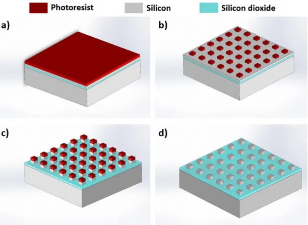
Figure 3.1: (a) Process flow for fabrication of silicon based 2D gratings utilizing SOI structure. First, 2.0 µm thick Si is thinned down to 1.2 µm Si. For simplicity, this step is not shown in the figure. After thinning the device Si layer, the rest of the patterning steps are explained in this illustration. (a) Spin coating of photoresist, (b) photolithography patterning, (c) etching of silicon by BOSCH process, (d) removal of photoresist with oxygen plasma.
3.2.2
Simulations
Electromagnetic wave simulations are performed using FDTD Solutions by Lumerical Inc, a commercially available FDTD simulation software package. For 3D simulation setup; on the x and y axes periodic boundary conditions are used, and on the z-axis (propagation direction) a perfectly matched layer (PML) is used. For 2D simulation setup; on the x-axis periodic boundary condition is used, and on the y-axis (propagation direction) PML is used. In all of the simulations, we employed cubic mesh with a mesh size of 10nm.
3.3
Results and discussions
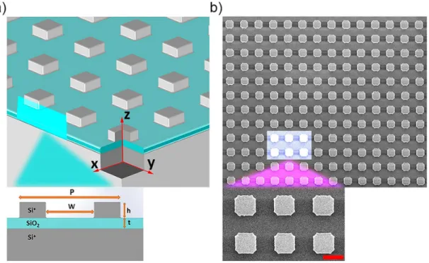
Figure 3.2a presents the schematic diagram of the wideband absorber. The ab-sorber is composed of a three-layer-stack of silicon-silicon dioxide-silicon struc-ture. Only the top silicon layer is patterned periodically along both x and y directions. For the fabrication of the structures, a commercially available silicon-on-insulator (SOI) wafer is utilized. Conventional optical lithography and deep reactive ion etching (DRIE) techniques are used for the microfabrication of the structures. The thicknesses of the silicon grating and the silicon dioxide layer are h=1.2 µm and t=0.8 µm, respectively. Two structures with different periodici-ties, P=7 µm and P=8 µm, and different widths, W=3 µm and W=4.2 µm, are implemented. Figure 3.2b shows the scanning electron microscope (SEM) image of the sample with periodicity, P=8 µm.
Figure 3.2: (a) Schematic representation of a three layer silicon-silicon dioxide-silicon structure with the top dioxide-silicon layer patterned as 2D gratings of periodicity P, (b) SEM image of one of the fabricated samples with periodicity, P=8 µm. Scale bar is 4 µm.
In order to conduct numerical analysis of these structures, we used finite differ-ence time domain (FDTD) method. Optical properties of highly-doped semicon-ductors are dominated by electron plasma of the material, and can be modeled us-ing Drude formalism [17,18]. The optical properties of the top and bottom silicon layers are extracted using Drude formalism. Our model is confirmed by means of an experimental setup. Doping concentrations of the top (n-type) and bottom (p-type) silicon layers are found to be Nn= 5.2×1019cm−3and Np = 5.5×1019cm−3,
respectively; and the relaxation frequencies are ωn = 0.04eV and ωp = 0.07eV ,
respectively. A characteristic frequency of semiconductors is called plasma fre-quency, which is defined as the frequency at which the real part of the permittivity vanishes. Plasma wavelengths of the top and bottom silicon layers are extracted to be λn = 8.28µm and λp = 9.42µm, respectively. In FDTD simulations
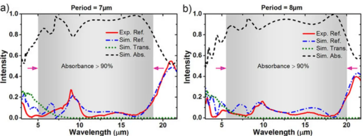
op-tical constants of silicon layers are taken from Drude formalism results and the optical constants of silicon dioxide are received from the literature [20]. The ab-sorption in the simulations is defined as A(λ) = 1 − R(λ) − T (λ), where T (λ) is the transmitted power and R(λ) is the reflected power. Figure 3.3 shows the simulated reflection, transmission, and absorption spectra at normal incidence for arbitrarily polarized light. In these computational analyses, transmitted power is calculated at 2.5 µm below the interface between silicon dioxide and bottom sili-con layer. Highly-doped silisili-con has a very high attenuation coefficient (1.61µm−1 at plasma wavelength, λ = 9.42µm), therefore almost no power is transmitted through the structure beyond plasma wavelength and only a weak transmission is observed at shorter wavelengths from simulation results. Plasma wavelength of the bottom silicon layer can be shifted to shorter wavelengths by increasing the doping density which will further decrease the transmitted power. Two different samples with periodicities of 7 µm and 8 µm provide absorption waveband of 5-18.8 µm and 5.4-20 µm, respectively; yielding excellent absorption performance that is more than 90 % in average. Red lines in Fig. 3.3a-b show the correspond-ing experimental reflection results of these wideband absorber structures and the measured reflection spectra agree well with the simulated ones.
The effect of multiple resonances can be identified from the absorption peaks in the spectra. In order to understand the nature of absorption processes we
Figure 3.3: (a,b) Simulated reflection (Sim. Ref.), transmission (Sim. Trans.) and absorption (Sim. Abs.) spectra and measured reflection (Exp. Ref.) spec-trum for the samples with periodicities of P=7 µm and P=8 µm.
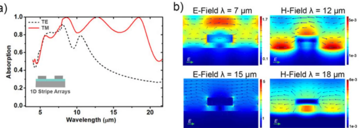
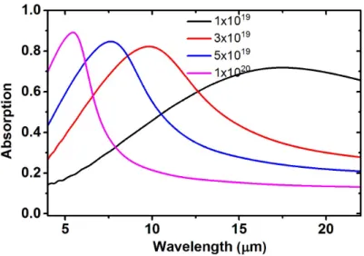
first investigated the absorption properties of one dimensional (1D) 1.2 µm-thick silicon stripes on 0.8 µm-thick silicon dioxide spacer on silicon substrate. The pe-riodicity and the fill ratio of the silicon stripe array are 8 µm and 0.5, respectively. Figure 3.4a shows the simulated normal incidence absorption spectra of this 1D structure for both TE (E-field is parallel to the silicon grating direction) and TM (E-field is perpendicular to the silicon grating direction) polarization configura-tions. For TE polarization, absorption between 6 µm and 9 µm is dominated by free carrier absorption in heavily doped silicon layers. This is the classical Drude absorption by free carriers and can be spectrally tuned by controlling the carrier concentration of silicon layers. Since the real part of the permittivity is very low around the plasma frequency, light can easily penetrate into the material. There-fore, reflection minimum and absorption maximum of a non-corrugated highly doped silicon occurs near the plasma frequency. Figure 3.5 shows the bulk ab-sorption of the 4 m thick silicon with different doping concentrations. As it seen in the graph, absorption peak blueshifts as the concentration increases.
Around 10 µm, silicon dioxide exhibits molecular resonance due to Si-O-Si vibrations. Asymmetric stretching vibration of Si-O-Si bridges contributes to the absorption in this region [41]. At longer wavelengths, free carrier conduction dominates, thus the reflectivity increases and the absorption decreases. For TM polarization, absorption spectrum gives the evidence for the excitation of surface
Figure 3.4: (a) Simulated absorption spectra of the 1D structure with periodicity 8 µm and fill ratio of 0.5 for TE and TM polarizations. Inset shows the schematic of 1D silicon silicon dioxide silicon structure (b) Calculated spatial field distri-butions for the same structure with periodicity of 8 µm at λ=7 µm, λ=12 µm, λ=15 µm, and λ=18 µm. The arrows represent the electric field vector.
plasmon modes. Two additional absorption peaks are observed at longer wave-lengths (at 12.7 µm and 18 µm) in addition to the absorption bands at shorter wavelengths.
Additional information can be obtained from spatial field distributions. Figure 3.4b shows the calculated field distributions at four major points in the absorption spectrum of the structure with periodicity, P=8 µm using the FDTD method. The electric field at 7 µm is mainly concentrated on the top of the silicon grat-ing, where incident field constructively interferes with the reflected field. At this range, field also penetrates through the silicon layers and is absorbed by free carriers. At wavelengths longer than the plasma wavelength, highly doped silicon layers behave like metals and the structure exhibits the properties of the common metal/insulator/metal (MIM) structures. Similar MIM structures consisting of a metal structure and a metal film separated by a dielectric layer were reported by several groups. These studies have shown the coupling between different plas-monic modes and investigated the effects of the structure periodicity, the fill ratio and the dielectric thickness on these plasmonic modes. When the periodicity of the structure is on the order of the wavelength, propagating surface plasmon res-onances can be generated. The magnetic field distribution at 12 µm shows strong confinement at the top of the silicon gratings and between two adjacent gratings.
Figure 3.5: Simulated absorption spectra of 4 µm thick silicon with different doping concentrations.
The field distribution at this range confirms that the absorption at this point arises from grating induced silica-side propagating surface plasmons (PSP). On the other hand, magnetic field at 18 µm is concentrated below the silicon grat-ings, in the gap filled by silicon dioxide. The absorption peak at this point is due to the gap-plasmon (GP) modes supported by the cavity between silicon layers as reported for similar MIM structures [42–48]. Electric field distribution at 15 µm shows strong confinement at the top and bottom of the silicon grating. Both PSP and GP modes have broad absorption bands (more than 5 µm), hence both of these modes have partial effects on the absorption at 15 µm.
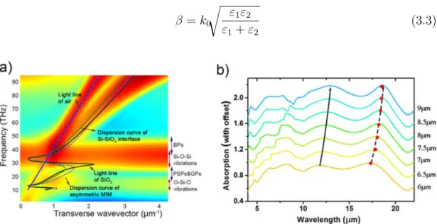
Dispersion relation of the surface waves supported by unpatterned Si-SiO2-Si-Air structure is calculated by using a bandstructure technique of the FDTD method. In this bandstructure technique we do a parameter sweep over the trans-verse wavevector and look for frequencies with strong resonances. Simulated dis-persion relation of this multilayer system is shown in Fig. 3.6a. Two vibrational bands of silicon dioxide, located at 13.6 THz (22 µm) and 30 THz (10 µm) [41], can be observed. Analytical dispersion relation of Metal/Insulator/Metal like structures are reported previously [49, 50]. The transverse magnetic plasmon dispersion relation for an asymmetric MIM structure is given by,
e−2k2t= k2/ε2+ k1/ε1
k2/ε2− k1/ε1
k2/ε2+ k3/ε3
k2/ε2− k3/ε3
(3.1)
where ε1, ε2, and ε3 represent the permittivities of the layers; bottom Si+,
SiO2, and top Si+, respectively. t is the gap thickness. k1, k2, and k3 are the
wavevectors perpendicular to the interfaces defined by momentum conservation:
ki2 = kspp2− k02εi (3.2)
for i=1, 2, and 3. kspp is the wavevector of the surface plasmons. Surface
plasmon polariton dispersion relation at a single interface is given by [51]:
β = k0
r ε1ε2
ε1+ ε2
(3.3)
Figure 3.6: (a) Simulated and analytical dispersion relation for the silicon-silicon dioxide-silicon-air structure. Abbr: BPs (Bulk Plasmons), PSPs (Propagating Surface Plasmons), GPs (Gap Plasmons). (b) Dependence of the absorption spectrum on the structure periodicity. Fill ratio is kept constant as 0.5 and the periodicity is varied from 6 µm to 9 µm.
Dispersion relation of MIM systems are implicit functions and can be solved numerically. Dashed blue line in Fig. 3.6a show the theoretical result for the
dispersion relation of silicon-silicon dioxide-silicon structure. Solid green line in the same figure represents the dispersion relation of propagating surface plasmons between silicon and silica. The plasmonic resonances, PSPs and GPs, are excited in the frequency range between the two vibrational bands of the silicon dioxide.
Figure 3.6b shows the simulated absorption spectra for various grating period-icities. In these simulations the fill ratio is kept constant as 0.5 and the periodicity is varied from 6µm to 9µm. Both of the plasmonic resonances show redshift with increasing periodicity. PSP mode (solid black line) is excited by periodic nature of the structure, so the resonance wavelength redshifts with increasing periodicity as expected. However, the resonance shift of GP mode essentially depends on the width of the silicon gratings rather than the periodicity. The constructive inter-ferences of GP mode, reflected back and forth at the edges of the cube, create a cavity resonance as in a Fabry-Perot interferometer. Therefore, the width of the silicon grating plays an essential role for the resonance shift as being a parameter of this cavity [42, 45, 47, 48]. GP resonance wavelength is related to the width of the silicon grating, w, by [42, 47, 49].
w2π
λ nef f = mπ − ϕ (3.4) where nef f is the effective index of the gap and can be calculated from
disper-sion relation, m is the mode order and ϕ is the phase of the reflection coefficient of the mode at the end of the gap. The reflection phase ϕ, zero for a perfect Fabry-Perot cavity, is nonzero for a finite waveguide and depends on the struc-ture and material properties [43, 48]. There is no analytical solution for reflection phase, hence it can be computed numerically or it is estimated as an average value minimizing the error of resonance wavelengths [42, 43, 47, 48]. In our structure we observe that the change in the reflection phase is nonsignificant when the fill ratio is kept constant. In order to determine reflection phase, we used one of the simulation results and we extracted the reflection phase as 63◦ according to the resonance wavelength in the simulation result. Since the reflection phase does not change significantly, all the other resonance wavelengths can be estimated
accurately by Eq. 3.4 for the first order resonance (m=1). As shown in Fig. 3.6b the simulated resonance wavelengths (dashed black line) almost match up with semi-analytically calculated (red circles) ones with an error less than 0.5%.
We also investigated the performance of the structure with periodicity 8µm and fill ratio 0.5 for different doping concentrations. Figure 3.7a shows absorp-tion spectrum as a funcabsorp-tion of doping density and wavelength. Dotted black line in the figure shows how plasma frequency shifts with increasing doping density. Due to the high penetration of field near the plasma frequency there exists an ab-sorption band following the plasma frequency line. Plasmonic abab-sorption bands (dashed white and dashed yellow lines) also shift to shorter wavelengths with increasing doping density. Blueshift of plasmonic absorption bands can be con-firmed by dispersion relations. Increasing doping concentration shifts dispersion curves to higher frequencies, thus excitation of plasmonic resonances occurs at shorter wavelengths. The blue rectangle shows the doping concentration range where ultra-broad absorption band can be obtained for this structure. Doping concentrations of silicon layers in the experimental part fall into this region.
In order to enrich our study and investigate further the origin of the plasmonic resonances we conducted angle-dependent simulations using the FDTD method. Figure 3.7b shows the evolution of the absorption spectra with increasing inci-dence angle. As shown in the figure, one of the plasmonic modes redshifts with the increasing incidence angle. The dependence of the plasmonic mode on the angle of incidence indicates that this is a propagating mode. As this resonance point shifts to longer wavelengths, vibrational absorption band of silicon dioxide becomes discernable around 10 µm. On the other hand, the other plasmonic mode around 18 µm as being a GP mode is almost independent of the incidence angle of the light. This is in agreement with previous studies done on similar systems by other groups [42, 45, 48]. Nearly all broadband absorbers are designed to absorb light independent of polarization and angle of incidence. In order to achieve a polarization-independent electromagnetic response we design our struc-ture to be symmetric in both x and y directions. Figure 3.7c shows the average absorption as a function of incidence angle for both TM (x-polarized, θ is in x-z plane) and TE (y-polarized, θ is in x-z plane) polarizations. At normal incidence,
Figure 3.7: (a) Absorption spectrum as a function of wavelength and doping density. (b) Absorption spectrum of the structure with periodicity 8 µm and fill ratio 0.5 for three different incidence angles. The structure is illuminated by a TM polarized plane wave. (c) Average absorption as a function of angle of incidence for TM and TE polarizations. (d) Absorption spectrum as a function of wavelength and angle of incidence.
the absorption spectra for both polarizations are the same because of the symme-try in the structure. For TM polarization average absorption is above 80% even at 70◦ angle of incidence and then it decreases dramatically. For TE polarization absorption is maintained around 80% at up to 50◦ angle of incidence. Figure 3.7d shows the extinction spectra as a function of wavelength and angle of incidence for the light composed of both TM and TE polarization components. As it is seen in the figure, the broadband response is maintained when the incidence angle smaller than 50◦, which is a significant achievement for resonant absorbers.
3.4
Conclusion
In conclusion, we have demonstrated ultra-broadband MID-IR absorbers on low-resistivity silicon. Periodically arranged silicon gratings are fabricated by using standard optical lithography and DRIE of silicon allowing for a cost-effective fab-rication of micro-scale structures. Two different structures with periodicities of 7 µm and 8 µm provide average absorptivity of more than 90% in the waveband of 5-18.8 µm and 5.4-20 µm, respectively, with a total thickness less than the quarter of the wavelength. The structures also exhibit broadband absorption performance even at high angles of incidence (θ=50◦) independent of the polarization. Our detailed analysis indicates that ultra-broadband light absorption originates from superposition of the free carrier absorption, and vibrational and plasmonic res-onances excited at different portions of the MID-IR range. Silicon-based strong and ultra-broadband absorption of light at MID-IR region is very promising for realization of silicon based infrared imagers, sensors, and enhanced spectroscopy. Combined with extensive processing and device design knowledge base of silicon, presented absorbers yield fabrication simplicity and CMOS compatible optoelec-tronic integration.
Chapter 4
Silicon based plasmonic surfaces
for sensing
This chapter will be based on the publication “High-conductivity silicon based spectrally selective plasmonic surfaces for sensing in the infrared region” K. Gorgulu et al., Journal of Optics, 19.2, (2016): 025002. Reproduced (or Re-produced in part) with permission from IOP Publishing. Copyright 2017 IOP Publishing.
4.1
Introduction
Plasmonic and metamaterial electromagnetic absorbers have attracted extensive attention not only for their fascinating electromagnetic properties, but also for their potential for various photonic applications. A perfect absorber absorbs all incident radiation at the frequency of operation by suppressing reflection, transmission and scattering in the structure. The first studies on metamaterial absorbers were in the microwave and THz regimes, utilizing two metallic layers separated by a dielectric layer [52–54]. Perfect absorption has been demonstrated with different types of unit cell structures such as patches, stripes and discs at
these wavelengths. A downscaling of unit cell dimensions allowed practical perfect absorbers at mid-infrared, near infrared and visible wavelengths with very high absorption efficiencies [55–57].
Carefully designed sub-wavelength metallic structures provide excitation of plasmonic and photonic resonances that show narrow absorption bands. Re-searchers tried to increase the absorption waveband by exploiting multiple res-onances simultaneously, for applications where broadband absorption is desir-able [4, 58]. However, some other applications, such as selective thermal emitters and detectors, and bio-chemical and refractive index sensors, require narrow ab-sorption bands [9,10]. Plasmonic absorbers typically have narrow resonance bands and therefore they can be utilized in spectrally selective detection schemes such as uncooled microbolometers [4]. According to Kirchhoff’s law of thermal radia-tion, a perfect absorber is equivalent to a good thermal emitter. In order to get a sharp emissivity peak, a narrowband absorber is required. Narrow resonance bands are also highly desirable in sensing applications in order to detect minute changes in the environment. Plasmonic resonances, confined to a metal dielec-tric surface, are extremely sensitive to the refractive index of the surrounding dielectric medium. Such strong dependency on the refractive index of the sur-rounding dielectric medium paves the way for ultra-sensitive label-free refractive index sensing applications [11, 12].
All examples mentioned above utilize conventional metallic components, such as gold and silver, as their material building blocks. In commonly used metals, the magnitude of the real part of the permittivity is very large at mid-infrared wavelengths. This feature of metals significantly limits their plasmonic mode confinement in the mid-infrared regime [13]. Conventional metals such as Ag also pose fabrication challenges and have degradation problems on exposure to air or humidity, limiting fabrication and integration of devices [14]. On the other hand, highly doped semiconductors are shown to exhibit plasmonic behavior in the mid-infrared regime [17, 24, 26, 59]. Compared to their metallic counterparts, highly doped semiconductors provide enhanced device performance, and fabrica-tion and CMOS integrafabrica-tion feasibility. Due to silicon’s prevailing manufacturing knowledge base, silicon plasmonics has received great attention. Localized surface
plasmon resonances excited on silicon nanowires synthesized via the vaporliquid-solid technique have been demonstrated [30]. Infrared absorption performance of a one-dimensional (1D) silicon grating and its possible application as a biological sensor have been studied computationally [32, 33]. Also, surface plasmon based thermal emission from patterned silicon has been studied experimentally [60].
In this paper we numerically and experimentally demonstrate frequency selec-tive infrared absorbers based on highly conducselec-tive silicon (p-type, ρ = 0.001 − 0.002Ω − cm). Furthermore, we demonstrate that the designed plasmonic devices are promising as efficient refractive index based sensing surfaces. We also study the dependence of sensing performance of our structure on the doping concentra-tion of silicon [61].
4.2
Structure and methods
Figure 4.1a presents a schematic representation of the proposed structures. Two-dimensional (2D) grating structures were patterned on a highly conductive silicon wafer using standard photolithography and reactive ion etching (RIE) techniques. First, we spun a photoresist, AZ 5214E at 4000 rpm, and baked it at 110 ◦C for 50 s. Then, we exposed the photoresist to a contact aligner and developed the photoresist with a deionized water diluted AZ 400 K developer. Silicon was patterned using a BOSCH process recipe that is SF6 based RIE at the etch
step, and C4F8 based deposition at the passivation step. Then, the remaining
photoresist was removed by an oxygen plasma cleaning recipe. Two structures with different periodicities, P = 8 µm and P = 9 µm, and different widths, W = 5.2 µm and W = 5.85 µm, were made. The height of the gratings is 1.4 µm. A top view scanning electron microscope (SEM) image of the 2D silicon absorber with periodicity P = 8 µm is shown in figure 4.1b. Reflection spectra from the fabricated samples were obtained using a Bruker HYPERION IR microscope and Bruker Vertex 70v Fourier transform infrared (FTIR) spectrometer with a gold mirror as the calibration reference.
Figure 4.1: (a) Schematic illustration of 2D grating structures. (b) Top-view scanning electron microscope image of the 2D plasmonic absorber structure with periodicity of P = 8 µm and fill ratio of 0.65. Scale bar is 10 µm. (c) Measured and simulated reflection from the flat silicon surface.
Optical properties of the highly conductive silicon can be modeled using the Drude formalism considering carrier density and mobility as the fitting parame-ters of the material [19, 27]. According to the model, carrier density and mobility of highly doped silicon used in this study were 7.5 × 1019cm−3 and 51cm2V−1s−1,
respectively. There is a characteristic transition wavelength called plasma wave-length which is defined as the wavewave-length at which the real part of the permittivity vanishes. The plasma wavelength of highly doped silicon substrates used in this study was calculated to be λpl = 8.2µm. At wavelengths longer than the plasma
wavelength, the real part of permittivity becomes negative and highly doped sil-icon behaves like a metal. Therefore, surface plasmons can be excited in this regime.
Electromagnetic wave simulations were performed using the finite difference time domain (FDTD) method by Lumerical Inc., a commercially available FDTD simulation software package. A three dimensional (3D) simulation setup is used;
on the x and y axes periodic boundary conditions are used. On the z-axis (prop-agation direction) a perfectly matched layer (PML) is used. In all of the simula-tions, we employ a cubic mesh with a mesh size of 10 nm.
We performed simulations and experiments for the reflection behavior of a flat silicon surface. The reflectance results from the simulation and experiment for a flat surface are given in figure 1(c). The simulation result and experimental measurement are in good agreement. The reflection results presented in figure 4.1c are also confirmed by analytical reflection calculations obtained by Fresnel’s equation.
4.3
Results and discussions
3D structures used in the FDTD simulations were imported from digitized SEM images of experimentally obtained 2D gratings. Figure 4.2a shows the calcu-lated and measured reflection spectra of the 2D plasmonic absorber structures for arbitrarily polarized light at normal incidence in the wavelength range from 7 µm to 20 µm. The 2D surface pattern gives a polarization insensitive optical response. The measured reflection spectrum for the 2D grating with period P = 8 µm shows approximately 98% absorption at the resonance wavelength. Such a near perfect absorption can be ascribed to efficient coupling of incident light into surface plasmon modes through momentum matching by diffraction. Considering normal incidence, in such grating structures the plasmon wavevector, is generally determined by the Bragg vectors associated with the grating periodicities. How-ever, because the structure dimensions are close to the wavelength of operation, resonance wavelength can be modified by the height and width of the gratings. As reported in a previous study, increasing the height of the grating leads to redshift in the resonance wavelength [60]. Structures with grating periodicities of 8 µm and 9 µm have reflection dips at 11.5 µm and 12.5 µm, respectively. Figure 4.2b shows a time-averaged magnetic field map for the structure with periodic-ity P = 9 µm at the resonance wavelength. As shown in the figure, magnetic field is strongly concentrated within the air trench surrounded by three highly
doped siliconair interfaces. Figure 4.2c shows the time-averaged power flow dis-tribution. The excitation of plasmonic resonance allows penetration of light into highly doped silicon and leads to strong optical absorption.
Figure 4.2: (a) Simulated and measured reflection spectra for structures with periodicities of P = 8 µm and P = 9 µm, and fill ratio of 0.65 for both struc-tures. (b) Cross section of the time-averaged magnetic field for the structure with periodicity P = 9 µm at the resonance wavelength. (c) Cross section of the time-averaged optical power flow vector distribution.
Angular reflection measurements were obtained using a J A Woollam IR-Vase spectroscopic ellipsometer. The optical response of the plasmonic absorbers for different angles of incidence were also calculated with the FDTD technique. Fig-ure 4.3 shows the reflection spectra for a 1D periodic sample in the case of three different angles of incidence. Simulated (dashed lines) reflectance spectra for the structures are in spectral agreement with experimental results (solid lines), but there are amplitude variations between measurement and experiment. For the simple 1D grating of grooves, phase-matching takes place whenever the condition β = ksinθ + νkx is fulfilled, where k is the wavevector of the light incident at an
angle θ, and ν = (1, 2, 3...). Therefore, increasing the angle of incidence redshifts the resonance wavelength. When the period increases, the effect of the recipro-cal vector reduces. Hence, angular sensitivity increases with increasing structure period.
Figure 4.3: Simulated and measured reflection spectra at three different incidence angles for the structure with P = 12 µm, fill ratio of 0.45 and height of 1.4 µm. The inset shows the fabricated 1D device structure.
We investigated the refractive index sensitivity of our plasmonic absorber structures by immersing the structure with periodicity P = 9 µm in acetone and measuring the reflection spectrum. In the sensing experiments, the liquid film thickness of acetone is about 200 µm (which is much greater than the penetration depth of surface plasmons into the material above the silicon surface [17]). The sensitivity of a surface plasmon resonance based sensor is defined as the change in resonant wavelength as a function of change in refractive index, S = ∆λ/∆n nm/RIU. Since it is easier to detect resonance changes with narrow lines, the sensitivity is divided into full-width at half-maximum (FWHM) to determine the figure of merit, FOM = S/FWHM. Figure 4.4a shows reflection spectra for the same structure in two different media, air and acetone, and the infrared reflec-tion spectrum of acetone. The refractive index of acetone is taken as 1.35 [62]. However, acetone has several molecular resonances over the entire mid-infrared region and the refractive index of acetone is modified in the vicinity of these resonance regions. In order to eliminate the effect of these resonances, reflection measurements of the plasmonic absorber under acetone are normalized to the infrared reflection spectrum of pure acetone. After normalization, molecular res-onances of acetone are alleviated but they are still discernable in the spectrum.
However, line-widths of these resonances are much smaller than the line-widths of the plasmonic resonances. Therefore, plasmonic (indicated by blue arrows) and molecular (indicated by red arrows) resonances can be distinguished eas-ily. We also simulated the reflection spectra for different refractive indices of the surrounding medium (Figure 4.4b). As depicted in figure 4.4b, the reflec-tion spectrum shows a gradual redshift with increasing refractive index values. Both measured and simulated resonance wavelengths as a function of refractive index of the surrounding medium are given in figure 4.4c. According to the linear fitting of the resonance frequencies, the sensitivity value is found to be approxi-mately 11 000 nm/RIU. Using this sensitivity value, the FOM value is calculated as 2.5. In general, the sensitivity of refractive index sensors is proportional to the operation wavelength. Therefore, the sensitivity of our absorber is very high compared to previous studies presenting their results at visible or near infrared regions [10, 12, 63–65]. However, in order to have a high FOM, the line-width of the resonance should be as small as possible. Even if our absorber has im-proved sensitivity, it has relatively low FOM values compared to the literature. It is important to note that reports of refractive index sensing applications on using conventional metals typically utilize either e-beam lithography or focused ion beam patterning. These techniques are costly and time-consuming for the fabrication of large-scale structures. Therefore, 1X contact photolithography and reduction photolithography based wafer scale fabrication of our silicon based sen-sors are promising for cost-effective applications.
The real and imaginary parts of dielectric permittivity of a semiconductor increase with doping concentration. Therefore, optical properties of a semicon-ductor become similar to those of traditional metals as the impurity concentration increases. We extracted optical properties of doped silicon using the Drude for-malism for doping values from 4 × 1019cm3 to 5 × 1020cm3. We considered the dependence of mobility on the carrier concentration in calculations of the opti-cal constants [66]. We investigated the dependence of the sensing performance on the doping density of silicon. We performed FDTD simulations for the same structure with different doping densities and two different refractive indices of the surrounding medium, n = 1 and n = 1.2. Figure 4.5a shows the simulated