Plasmonically Enhanced ZnO Thin-Film-Photo-Transistor with
Dynamic Responsivity Control
Ayşe Özcan1,*, Enes Battal1,2, Fatih Bilge Atar1,2 and Ali Kemal Okyay1,2 1
UNAM - Institute of Materials Science and Nanotechnology, Bilkent University, TR-06800, Ankara, Turkey
2
Bilkent University, Department of Electrical and Electronics Engineering, Bilkent, TR-06800, Ankara, Turkey
*Tel: +90 (312) 290 1557, e-mail: [email protected] Abstract- We fabricated an ZnO based thin-film
photo-transistor with electrically tunable photo-responsivity operating in the UV and visible spectra and designed plasmonic structures enhancing the device performance up to 6 folds below the band-gap of ZnO.
I. INTRODUCTION
Recently, Zinc-Oxide (ZnO) based thin film transistors (TFTs) attracted much attention due to their potential of replacing amorphous Silicon (ɑ-Si) which is used widely for conventional TFTs [1]. Especially, higher mobility of ZnO compared to ɑ-Si makes it more plausible for TFT applications [2]. Several techniques are used to deposit ZnO channel layer of transistors including RF magnetron sputtering [3], chemical vapor deposition [4], molecular beam epitaxy (MBE) [5], laser ablation [6] and atomic layer deposition (ALD) [7] techniques. Among these techniques, ALD comes forward with high quality film growth, high-precision thickness control and large area application advantages [7].
Along with its supreme electrical properties, ZnO has been started to use as an active layer for optoelectronic applications. ZnO has a strong absorption up to the wavelength of about 375nm [8] due to its band-gap of 3.31eV. However, ALD grown ZnO has considerable amount of traps that give rise absorption in the visible spectrum observed in the previous photoluminescence studies [8]. ZnO based light emitting diodes[9], detectors [4], solar cells [10] and photo-transistors [11] have been realized in this spectrum. Yet, the performance of such devices has been limited to bulk absorption properties of ZnO layers.
In recent years, many methods have been developed to improve the performance of photodetectors and photo-voltaic devices. Surface plasmons, collective oscillations of electrons coupled with electromagnetic waves, have been proven to be very useful at ultra-violet and visible spectrum for increasing device absorption [12]. In order to maximize absorption, localized and propagating surface plasmons excited by nanoparticles or gratings are very useful due to their immense subwavelength scaling properties.
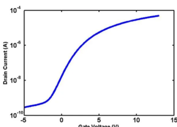
Figure 2 – At 0.5V of drain to source voltage (VDS), contrast ratio of about 104 and turn on voltage of -2V is observed in drain-source current to gate voltage (IDS-VGS) relation of the fabricated device.
In this work, we demonstrate a plasmonically enhanced ZnO based thin film photo-transistor (TFPT). We fabricated and characterized an ALD grown ZnO based TFPT operating at ultraviolet and visible wavelengths. We electrically characterized transistor characteristics of the fabricated device and we performed optical responsivity measurements. We designed metallic gratings enhancing overall photo-response of the fabricated device up to 6 fold in the wavelength range of 400 - 600nm.
II. EXPERIMENT
The device fabrication by deposition of a SiO2 contact isolation layer with plasma enhanced chemical vapor deposition on a p-type highly doped Si substrate. This layer is patterned with optical lithography and etched with buffered oxide etchant (BOE). Then, an Al2O3 gate oxide layer is deposited at 250°C for 200 cycles with Cambridge Savannah 100 ALD System using tri-methyl-aluminum and water precursor. A 100cycles of ZnO channel layer is deposited at 250°C using diethyl-zinc and water. The ZnO layer is patterned with optical lithography and etched with dilute H2SO4 solution.
After an optical lithography process, a 100nm thick Al drain and source layer is deposited followed by lift-off. The finalized structure is depicted in Figure 1.
The fabricated transistors are electrically characterized by Keithley 4200-SCS semiconductor parameter analyzer system. The drain-source current to gate voltage (IDS-VGS) is plotted in Figure 2 for 0.5V drain to source (VDS) bias. The turn on gate voltage, VON, andthe ON/OFF ratio, ION/IOFF are determined to be -2V and 104, respectively. Threshold voltage of this device
is extracted from the √ -VGS relation as 1V. From the log IDS
-VGS curve, the sub-threshold slope of the device is determined to be 1.17 V/dec.
Figure 1 a) 3-dimensional depiction of the plasmonically enhanced ZnO based photo-transistor device structure
343
WA1.2 (Contributed)
9:00 AM – 11:30 AM
Under a modulated illumination with a mechanical chopper at a frequency of about 375Hz and a lock-in amplifier, we measured the responsivity, defined as ratio of the photocurrent
(IDS) to incident optical power. Figure 3 shows the responsivity
of the photo-transistor under different gate bias voltages. Applying reverse bias from the gate depletes the trapped carriers and allows more absorption in the visible region. In this way, the photo-response from the photo-transistor can be controlled by applying different gate-bias. Yet, the responsivity in the spectral region below the band-gap remains low comparing to the region above band-gap.
III. SIMULATION RESULTS
In order to increase the responsivity of the device in the visible region, we integrate rectangular plasmonic structures on top of the active ZnO layer as shown in Figure 1. We performed 2-dimensional finite difference time domain simulations using FDTD solutions from Lumerical Inc. The rectangular gratings are assumed to be placed periodically. The height of the rectangular grating is kept constant at 100nm, whereas, width (w) and distance (d) parameters are swept for optimization. The refractive index of ZnO and Al2O3 layers are obtained using a spectroscopic ellipsometer (JaWoollam V-Vase). For Al and Si layers, optical constants from literature data [] are used. We compared the absorption inside the active ZnO layer for the case with and without plasmonic gratings assuming a light polarization suitable for plasmon excitation i.e. electric field vector is normal to the gratings. We also investigated the effect of metallic gratings, experimentally.
In Figure 4a, overall absorption enhancement integrated over 400-600nm spectrum is depicted. The optimum structure parameters are found to be w=90nm and d=125nm with an overall enhancement of about 7 times. Spectral absorption enhancement for the optimum structure is depicted in Figure 4b. The highest enhancement is observed at the wavelength where the plasmon resonance is much stronger near the
ZnO/Al interface as can be seen from the electric field intensity profile in Figure 5a. Absorption enhancement is attributed to localized surface plasmon (LSP) resonance excited at the ZnO/Al interface which is weakly coupled to the LSP mode excited at air/Al interface. H field intensity profile in Figure 5b indicates that the plasmonic structure acts like a strong forward scatterer.
IV. CONCLUSION
We fabricated an ALD grown ZnO based thin film photo-transistor (TFPT) and designed plasmonic grating structure exhibiting overall performance enhancements up to 6 fold in the overall spectrum of 400-600nm. We predicted that the responsivity in the spectral region below the band-gap can be increased up to the values of the responsivity in the region above band-gap. This study paves the way of realizing efficient photo-transistors operating in the UV and visible region.
ACKNOWLEDGEMENTS
This work was supported in part by European Union Framework Program 7 Marie Curie IRG Grant 239444, COST NanoTP, TUBITAK Grants 109E044, 112M004 and 112E052. The authors acknowledge support from TUBITAK-BIDEB.
REFERENCES
[1] R. L. Hoffman, B. J. Norris, and J. F. Wager, Applied Physics Letters, vol. 82, pp. 733-735, 2003.
[2] E. Fortunato, P. Barquinha, and R. Martins, Advanced Materials, vol. 24, pp. 2945-2986, 2012.
[3] P. F. Carcia, R. S. McLean, M. H. Reilly, and J. G. Nunes, Applied Physics
Letters, vol. 82, pp. 1117-1119, 2003.
[4] Y. Liu, C. R. Gorla, S. Liang, N. Emanetoglu, Y. Lu, H. Shen, et al.,
Journal of Elec Materi, vol. 29, pp. 69-74, 2000/01/01 2000.
[5] Y. Chen, D. M. Bagnall, H.-j. Koh, K.-t. Park, K. Hiraga, Z. Zhu, et al.,
Journal of Applied Physics, vol. 84, pp. 3912-3918, 1998.
[6] M. Hiramatsu, K. Imaeda, N. Horio, and M. Nawata, Journal of Vacuum
Science & Technology A: Vacuum, Surfaces, and Films, vol. 16, pp. 669-673,
1998.
[7] S. Lee, Y. Im, and Y.-B. Hahn, Korean J. Chem. Eng., vol. 22, pp. 334-338, 2005/03/01 2005.
[8] L. E. Aygun, F. B. Oruc, F. B. Atar, and A. K. Okyay, Photonics Journal,
IEEE, vol. 5, pp. 2200707-2200707, 2013.
[9] Y. Ryu, T.-S. Lee, J. A. Lubguban, H. W. White, B.-J. Kim, Y.-S. Park, et
al., Applied Physics Letters, vol. 88, p. 241108, 2006.
[10] I. Repins, M. A. Contreras, B. Egaas, C. DeHart, J. Scharf, C. L. Perkins,
et al., Progress in Photovoltaics: Research and Applications, vol. 16, pp.
235-239, 2008.
[11] H. S. Bae, M. H. Yoon, J. H. Kim, and S. Im, Applied Physics Letters, vol. 83, pp. 5313-5315, 2003.
[12] D. K. Gramotnev and S. I. Bozhevolnyi, Nat Photon, vol. 4, pp. 83-91, 2010.
Figure 3 - The responsivity of the device is controlled by applying different gate bias voltages. The responsivity for the region below the band-gap is much lower than that of the region above band-gap.
Figure 4 - a) Dependence of overall enhancement for 400-600nm spectrum on the structure parameters, distance (d) and width (w). b) For the optimum structure, spectral absorption enhancement is depicted
Figure 5 – Electric and magnetic field intensity profiles at the wavelength of highest absorption ehnancement (600nm).