A MEMS T/R Switch Embedded in CMUT
Structure for Ultrasound Imaging Frontends
Xiao Zhang
∗, Arooba Zeshan
†, Oluwafemi J. Adelegan
∗F. Yalcin Yamaner
†, and ¨
Omer Oralkan
∗ ∗Department of Electrical and Computer Engineering, North Carolina State University, Raleigh, NC, USA †Department of Electrical and Electronics Engineering, Istanbul Medipol University, Istanbul, TURKEYEmail: [email protected]
Abstract—This paper describes a novel MEMS trans-mit/receive (T/R) switch that could be embedded in the general structure of a capacitive micromachined ultrasonic transducer (CMUT). A MEMS switch and a CMUT element were fabricated side by side using an anodic-bonding-based fabrication process. The plates of the CMUT and the membrane-type switch were formed at the same step by anodic bonding. A single switch was tested in air for preliminary characterization. Vacuum-sealing of the switch cell was confirmed by an atmospheric deflection measurement. The switch was then biased at 59-V DC voltage and turned on and off by applying a 1-kHz, 5-Vppsquare wave to the
control terminal while a 1-MHz, 300-mVppsinusoidal signal was
applied at the RF input. The signal measured at the RF output demonstrates the basic switching behavior with a switch series resistance of 124 Ω. This work is important for the ultrasound imaging system efficiency and could significantly ease the high-voltage requirements of frontend circuits.
Index Terms—CMUT; MEMS switch; Anodic bonding; Ultra-sound system; Glass.
I. INTRODUCTION
Transmit/receive (T/R) switches are critical components in an ultrasound imaging system, which is switched back and forth between the transmission and reception modes during imaging. A T/R switch connects the transducer to the trans-mitter while isolating the receiver during the transmission cycle. Similarly, the T/R switch connects the transducer to the receiver while isolating the output of the transmitter during the receiving cycle. For ultrasound frontends the switching time of a few hundreds of nanoseconds is desired so that the dead zone in front of the transducer can be minimized. The current switch implementations are based on electronic components such as diodes and field-effect transistors [1]. A common implementation is based on using a diode bridge or cross-coupled diode pair [2]. This implementation deviates from the ideal switching behavior as it introduces noise and distortion in the receive path and fails to completely isolate the receiver input from the transmit pulse causing some extended dead zone in the near field.
A MEMS switch has the potential to provide high isola-tion in the open state and low inserisola-tion loss in the closed state. However, MEMS switches are often designed for RF applications, where fast switching speed is not a requirement,
This work was supported by the National Institutes of Health under grant EB021010.
and therefore are not suitable for an ultrasound frontend [3]. CMUTs and MEMS switches are both electrostatically actuated capacitors with a moving plate and share similar fabrication technologies. Although the integration of these two components seems a natural decision, there has been no demonstration of CMUTs with embedded MEMS T/R switches. This work investigates a fast-switching, low-control-voltage, DC-contact-mode series MEMS switch that can be integrated and co-fabricated with CMUTs using our previously reported anodic-bonding-based process [4].
In the following section, we first present the design and the fabrication process flow. In Section III, a fabricated switch test structure is characterized.
II. DESIGN ANDFABRICATION
Since the basic building block of a CMUT is a parallel plate capacitor that pulls in due to mechanical instability at a certain electrical field, an electro-mechanical switch can be easily embedded in the CMUT structure. The electrostatic force that pulls down CMUT plate is also what makes a MEMS switch work.
It has been reported that the switching time is mainly deter-mined by the device mechanical resonant frequency f0[5]. For
an inertia-limited system (with a small damping coefficient and Q>2), the switching time ts depends on the device resonant
frequency f0, pull-in voltage Vp, and actuation voltage Vs, as
shown in Eq. 1.
ts≈ 3.67
Vp
Vs2πf0
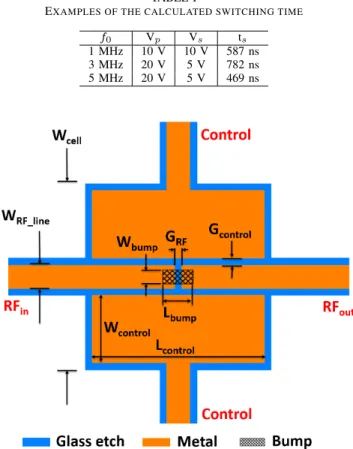
(1) The vacuum-backed membrane structure with small di-mensions gives CMUTs the ability to make devices with MHz resonant frequencies which translate to fast switching. Considering that the CMUT resonant frequency for medical applications is usually in the range of several MHz, pull-in voltage is in the range of tens of volts, Table I presents several examples of fast switching time assuming typical CMUT operation parameters.
The design of the presented MEMS switch here is based on a single CMUT cell. Fig. 1 shows the layout design of a switch cell. When a DC voltage is applied on the control electrodes, the electrostatic force pulls the membrane down and a metal protuberance on the bottom surface of the plate of the switch cell connects the RF line.
978-1-4673-9897-8/16/$31.00 ©2016 IEEE 2016 IEEE International Ultrasonics Symposium Proceedings
TABLE I
EXAMPLES OF THE CALCULATED SWITCHING TIME
f0 Vp Vs ts
1 MHz 10 V 10 V 587 ns 3 MHz 20 V 5 V 782 ns 5 MHz 20 V 5 V 469 ns
Fig. 1. The layout design of the switch.
The fabrication process flow is shown in Fig. 2. The first cell on the left represents the switch. The other three cells represent the co-fabricated CMUT element. The initial glass substrate was a 0.7-mm thick, 100-mm diameter borosilicate glass wafer (Borofloat R33, Schott AG, Jena, Germany) (Fig.
2a). First, the substrate was cleaned using a piranha solution for removal of organics and other contaminants. Then the cavities of the switch and the CMUT were patterned at the same time. We performed reactive ion etching to define a cavity depth of 350 nm (Fig. 2b). The photoresist was then removed and the bottom metal pattern was defined by a second photolithography step using a 2-µm-thick negative photoresist. A stacked metal that consists of 20-nm chromium and 100-nm gold was formed in the etched cavities by evaporation and lift-off (Fig. 2c). The metal layer serves as the bottom electrode for the CMUT and also control electrodes and RF line for the switch. Fig. 3a shows the optical image of the switch and the CMUT after the completion of process on the glass substrate. The CMUT bottom electrode is connected to the switch RF line. Fig. 4a shows the AFM image depicting the center region of the switch cell.
Next, we deposited a 200-nm PECVD silicon nitride insula-tion layer on the device layer of the SOI wafer. The insulainsula-tion layer prevents the short circuit when the CMUT pulls in. The insulation layer is also needed for the switch because the bump should be insulated from the top plate electrode. The bump
(a) (b) (c) (d) (e) (f) (g) (h)
Fig. 2. Fabrication process flow: (a) Initial glass substrate; (b) Photolithog-raphy and glass etch; (c) Metal deposition and lift-off; (d) Silicon nitride deposition and metal bump formation on the SOI wafer and anodic bonding with alignment; (e) Handle wafer and BOX removal; (f) Silicon/silicon nitride etch for gas evacuation, top electrode separation, reaching bottom electrode, and device separation; (g) Silicon nitride deposition for sealing; (h) Silicon nitride etch and metallization.
(a) (b)
(c) (d)
Fig. 3. Optical images of the switch and CMUT combination. (a) After glass etch, bottom electrode deposition, and lift-off; (b) After anodic bonding and handle/BOX removal. A close-up view shows the metal bump aligned to the RF line gap; (c) After plate etch and gas evacuation; Switch and CMUT top electrodes are isolated; (d) After silicon nitride sealing, sealing nitride etching, and metalization.
can then be formed on the insulation layer by evaporating and lifting off a stacked metal layer of 20-nm chromium and 50-nm gold (Fig. 4b). The processed glass and SOI wafers were first aligned and then anodically bonded at 350◦C under 2.5-kN down force in vacuum (10−4 Torr) using an in-situ aligned wafer bonding system (Model AML-AWB-04, Applied Microengineering Ltd, Oxfordshire, United Kingdom) (Fig. 2d). The handle layer of the SOI wafer was ground down to 100 µm. The remaining handle layer and the BOX layer were removed using a heated tetramethylammonium hydroxide solution (10% TMAH at 80◦C) and a 10:1 BOE solution, respectively (Fig. 2e). Fig.3b displays the optical image that shows the bonded SOI device layer as the plate and a close-up view of the aligned metal bump over the RF line.
In the next step, we dry-etched the silicon/silicon nitride plate (Fig. 2f). This step serves the following purposes. First, it evacuates the generated gas during anodic bonding in the switch and CMUT cells, so that the cells could be later sealed in vacuum. Second, it isolates the top electrode plate of the switch and the CMUTs to enable independent biasing of the CMUT and the switch cell. Third, it allows to access the bottom pads of the switch and CMUTs. Additionally, this step defines the dicing lines for device separation. After the etching, the photoresist was removed using oxygen plasma. Fig. 3c shows the optical image after this step.
We deposited 800-nm conformal PECVD silicon nitride on the entire wafer surface to seal the cavities (Fig. 2g). After that, the silicon nitride needs to be etched in order to access the bottom electrodes. The sealing silicon nitride was only left
(a) (b)
Fig. 4. (a) AFM image showing the center region of the switch bottom metal. (b) AFM image showing the metal bump defined on the silicon nitride insulation layer on top of the SOI device layer.
at the places where sealing is needed. Then we transferred the wafer to the evaporation chamber without removing the photoresist. Finally, a stacked layer of 20-nm chromium and 180-nm gold was evaporated and lifted off to form electrical contacts (Fig. 2h). Fig. 3d shows the optical image of the final device.
III. CHARACTERIZATION
The physical parameters of the fabricated switch is shown in Table II. The success of the sealing process was confirmed by measuring the atmospheric deflection of the switch top plate after the completion of the entire process (Fig. 5). The deflection was measured as 43 nm.
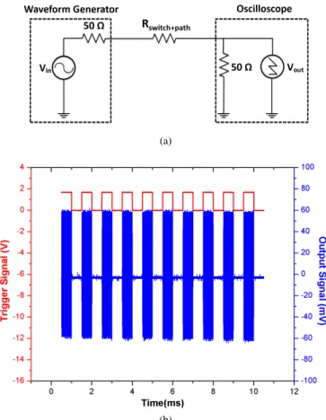
A switch test structure was tested in air under a probe station (Fig. 6). A DC power supply was used to apply a bias voltage of 59 V to the control electrodes. Then a 5-Vpp, 1-kHz
square wave was superimposed on the DC bias to control the switch. A 1-MHz, 300-mVpp sinusoidal wave was applied by
a function generator to the RF input. The RF output signal was recorded by an oscilloscope. Fig. 7a shows the diagram of the experimental setup. Fig. 7b shows the measured output signal. The switch resistance in series with the metal path resistance is calculated as 149 Ω. Given the RFin to RFout
metal path resistance is 25 Ω, the switch series resistance
TABLE II
PHYSICAL PARAMETERS OF THE TESTED SWITCH
Horizontal dimensions
Shape of the cell Square Cell width, Wcell 80 µm
Control electrode width, Wcontrol 29 µm
Control electrode length, Lcontrol 74 µm
Bump width, Wbump 6 µm
Bump length, Lbump 13 µm
RF line width, WRF line 10 µm
Ctrl electrode to RFlinegap, Gcontrol 3 µm
RF line gap, GRF 3 µm
Vertical dimensions
Substrate thickness, 700 µm Glass etching depth, 0.35 µm Bottom metal thickness, 0.15 µm Bump thickness, 0.07 µm Insulation layer thickness, 0.2 µm
Silicon plate thickness, 2 µm Top metal thickness, 0.2 µm
Fig. 5. The atmospheric deflection of the switch cell.
(a) (b)
Fig. 6. (a) Fabricated switch test structure. (b) Connection setup under a probe station.
is 124 Ω, which could be reduced by optimizing the switch geometry. The results demonstrate that the fabricated switch is promising for ultrasound imaging applications.
IV. CONCLUSION
We presented a MEMS T/R switch that is co-fabricated with a CMUT element on the same substrate using anodic bonding. A switch test structure was characterized. The atmospheric deflection measurement confirmed that fabricated switch is vacuum-sealed. A preliminary measurement shows the switch could be turned on and off by a 5-V, 1-kHz control signal to conduct and block a 1-MHz sinusoidal input signal. The series switch resistance is measured as 124 Ω, which could be reduced by optimizing the switch geometry. This work demonstrates that the co-fabricated MEMS T/R switch in a CMUT element has a great potential to impact ultrasound imaging frontends.
ACKNOWLEDGMENT
The fabrication was performed in part at the NCSU Nanofabrication Facility (NNF), a member of the North Car-olina Research Triangle Nanotechnology Network (RTNN), which is supported by the National Science Foundation (Grant ECCS-1542015) as part of the National Nanotechnology Coor-dinated Infrastructure (NNCI). The device characterization was
(a)
(b)
Fig. 7. (a) Diagram of the experiment setup. (b) 1-MHz input signal turned on and off by a 1-kHz control signal.
performed in part at the Analytical Instrumentation Facility (AIF) at North Carolina State University, which is supported by the State of North Carolina and the National Science Foundation (award number ECCS-1542015). The AIF is a member of the North Carolina Research Triangle Nanotechnol-ogy Network (RTNN), a site in the National NanotechnolNanotechnol-ogy Coordinated Infrastructure (NNCI).
REFERENCES
[1] J. Camacho and C. Fritsch, “Protection circuits for ultrasound applica-tions,” IEEE Trans. Ultrason., Ferroelect., Freq. Contr., vol. 55, no. 5, pp. 1160–1164, 2008.
[2] A. Nikoozadeh, ¨O. Oralkan, M. Gencel, D. N. Stephens, A. de la Rama, P. Chen, K. Thomenius, A. Dentinger, D. Wildes, K. Shivkumar, A. Mahajan, M. O’Donnell, D. Sahn, and P. T. Khuri-Yakub, “Forward-looking volumetric intracardiac imaging using a fully integrated CMUT ring array,” in Proc. IEEE Ultrason. Symp., 2009, pp. 511–514. [3] G. M. Rebeiz and J. B. Muldavin, “RF MEMS switches and switch
circuits,” IEEE Microwave Magazine, vol. 2, no. 4, pp. 59–71, 2001. [4] F. Y. Yamaner, X. Zhang, and ¨O. Oralkan, “A three-mask process for
fab-ricating vacuum-sealed capacitive micromachined ultrasonic transducers using anodic bonding,” IEEE Trans. Ultrason., Ferroelect., Freq. Contr., vol. 62, no. 5, pp. 972–982, 2015.
[5] G. M. Rebeiz, RF MEMS : theory, design, and technology. J. Wiley, 2003.