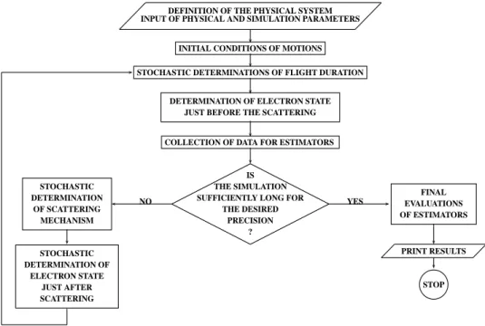
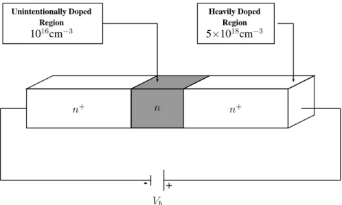
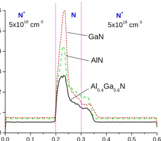
High field transport phenomena in wide bandgap semiconductors
Tam metin
Şekil


Benzer Belgeler
Interior architecture students’ attitude toward the use of computers in the design phase of architectural design process is positive4. Male students’ attitude toward the use
This paper describes the control of gas generator pressure in throttleable ducted rockets using nonlinear adaptive control as well as classical control approachesI. Simulation
Kaplan’a göre Türk milletinin kültürel değerleri şunlardır: Türk Dili, Türk Ede- biyatı, Türk Tarihi, Türk Mûsikîsi, Türk Plâstik Sanatları, Türk Şehirleri
In summary, based on average percent deviations from optimality, move based heuristics (M/I and M) perform better than the pairwise interchange method (I)... In
Bu yaz›da, meddah anlat›lar›ndan biri olarak kabul edilen T›flî Efendi’nin estetik özelliklerinin ön plana ç›kar›lmas› ve onun tikel bir metin olarak
As well as the sympathy we have for others’ physical sufferings which is defined by Grouchy as the sympathy we are naturally inclined to show because the physical suffering is
Marmara Üniversitesi’nde lisans programında Genel Jeoloji, Mineral ve Kayaçlar, Hidrografya, Yapısal Jeomorfoloji, Coğrafya Araştırmaları, Türkiye Hidrografyası,
widespread defects in cutaneous epithelium, and also affects the epithelial lining of the oral cavity, especially the tongue... The condition is characterized by
