PROCEEDINGS OF SPIE
SPIEDigitalLibrary.org/conference-proceedings-of-spieMIMIM photodetectors using
plasmonically enhanced MIM
absorbers
S. Abedini Dereshgi, A. K. Okyay
S. Abedini Dereshgi, A. K. Okyay, "MIMIM photodetectors using plasmonically
enhanced MIM absorbers," Proc. SPIE 10099, Physics, Simulation, and
Photonic Engineering of Photovoltaic Devices VI, 100991C (23 February
2017); doi: 10.1117/12.2253026
Event: SPIE OPTO, 2017, San Francisco, California, United States
Downloaded From: https://www.spiedigitallibrary.org/conference-proceedings-of-spie on 12/16/2018 Terms of Use: https://www.spiedigitallibrary.org/terms-of-useillumination Ag nanoparticles
+
1
-0
AI203(40nm)
o
MIMIM Photodetectors Using Plasmonically Enhanced MIM
Absorbers
S. Abedini Dereshgi
a,b, A. K. Okyay
*a,b,ca
Department of Electrical and Electronics Engineering, Bilkent University, Bilkent, Ankara, Turkey;
bNational Nanotechnology Research Center (UNAM), Bilkent University, Bilkent, Ankara, Turkey;
c
Institute of Materials Science and Nanotechnology, Bilkent University, Bilkent, Ankara, Turkey
ABSTRACT
We demonstrate super absorbing metal-insulator-metal (MIM) stacks and MIMIM photosensitive devices operating at visible and near-infrared (VIS-NIR) spectrum, where absorbing (top) MIM and photocollecting (bottom) MIM can be optimized separately. We investigate different bottom metals in absorbing MIM with nanoparticles realized by dewetting of silver thin film on top. While gold and silver have conventionally been considered the most appropriate plasmonic absorbers, we demonstrate different absorbing metals like aluminum and specifically chromium, with its plasma frequency happening at 850 nm, as more efficient layers for absorption. Absorption in chromium hits 82 percent around 1000 nm. We provide convincing evidences by doing reflection experiment and computational simulations for absorbing MIM part. We also suggest for the first time investigating electric loss tangent of metal or coherently, surface plasmon quality factor of absorbing metals which are reliable tools for engineering different metal layers. They reveal that despite the fact that gold and silver are good plasmonic scatterers in VIS-NIR and reliable absorbers in VIS region, they are not proper choices as absorbers for NIR applications. Once the most optimum absorbing design is pointed out, we integrate it on top of another metal-insulator to form an MIMIM photodetector with tunneling photocurrent path. The final optimized sample consisting of silver – hafnium oxide – chromium – aluminum oxide – silver nanoparticles (from bottom to top) has a dark current of 7nA and a photoresponsivity peak of 0.962 mA/W at 1000 nm and a full width at half maximum of 300 nm, while applied bias is 50 mV and device areas are 300 μm x 600 μm. This photoresponse shows 70 times enhancement compared to former reported spin coated rare nanoparticle MIMIMs.
Keywords: Plasmonic absorber, MIMIM, photovoltaic, photodetectors, photoresponsivity, tunneling, dewetting.
1. INTRODUCTION
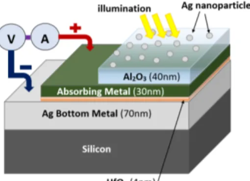
With an increasing trend of mobile photovoltaics (PV), plasmonic structures are potential candidates in providing low cost ultra-thin PV devices. Dewetting method for producing nanoparticles has numerous advantages like its low cost, easy fabrication and broader absorption spectrum compared to other common expensive methods like electron beam lithography and focused ion beam writing. Metal-insulator-metal (MIM) absorbers have attracted attention in recent years [1, 2]. Some MIM stacks are reported which carry the burden of both good absorption and efficient photocurrent generation [3]. This would put restrictions on engineering such stacks to be optically and electrically well-performing. Metal-insulator-metal-insulator-metal (MIMIM) stacks, on the other hand, facilitate integrating the absorbing top MIM part with the electrical photocarrier collection part to form a complete photodetector [4] (Fig. 1).
Figure 1.Schematic of MIMIM photodetector.
Physics, Simulation, and Photonic Engineering of Photovoltaic Devices VI, edited by Alexandre Freundlich, Laurent Lombez, Masakazu Sugiyama, Proc. of SPIE Vol. 10099, 100991C · © 2017 SPIE
CCC code: 0277-786X/17/$18 · doi: 10.1117/12.2253026 Proc. of SPIE Vol. 10099 100991C-1
Downloaded From: https://www.spiedigitallibrary.org/conference-proceedings-of-spie on 12/16/2018 Terms of Use: https://www.spiedigitallibrary.org/terms-of-use
In this work, first we focus on engineering broadband MIM absorbers followed by the design of tunneling MIM junctions to optimize the carrier collection. We are interested in functionality in NIR region due to the fact that for VIS region, there are industrialized highly efficient absorbers using silicon already.
Obviously, it is crucial to have absorption in the middle metal for a photovoltaic MIMIM device. Chromium and aluminum are among the metals with highest absorptivity. While chromium has been neglected as a plasmonic absorber to the best of our knowledge, we prove that it is an eminent metal for NIR photovoltaic devices for the first time. This is quite contradictory to the status quo choices of plasmonic metals gold and silver as absorbers in VIS-NIR region.
2. RESULTS AND DISCUSSION
2.1 Dewetting
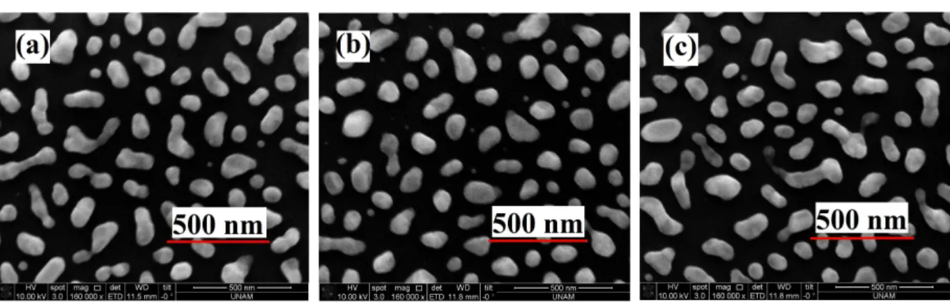
In some metals like gold and silver, when deposited thin enough, the metal-air interfaces will not be stable. If the thickness is in the order of 10 nm, the film is in thermodynamically metastable state meaning that under some excitation, the film will agglomerate in islands to minimize the surface with air, called the dewetting process. The excitation for dewetting to take place is applied using rapid thermal annealing (RTA) system. In order to obtain optimized recipe for desirable distribution of nanoparticles, heating and cooling rates are studied for silver thin films. Silver films formed more uniform particles in our experiments compared to gold. Our initial simulations indicated that particles of 100 nm in size and intermediate distance of 200 nm will result in acceptable absorption in the middle (absorbing) metal. After initial examination, we recognized 10 nm thin silver film is a reasonable choice. We applied three different recipes using Eurotherm RTA system to roughly attain the mentioned distribution, the SEM images of which are represented in Fig. 2.
Figure 2. SEM image of silver nanoparticles after applying 500◦C heat for 20min with (a) heating rate of 100 ◦C/min and cooling rate of 100 ◦C/min, (b) heating rate of 100 ◦C/min and cooling rate of 500◦C/min and (c) heating rate of 500 ◦C/min and cooling rate of 500◦C/min respectively.
Comparing Figs. 2. (a), (b) and (c) it can be deduced that the most detrimental effect comes from rapid heating of film. Therefore, rapid heating and rapid cooling (Fig. 2 (c)) result is dropped out. Besides, comparing the remaining SEM images, we conclude that rapid cooling results in small residues that add up to non-uniformity. However, overall uniformity is higher in Fig. 2 (b) and it is preferable to neglect small residues in favor of more uniformity. Thus, the optimized recipe is deposition of 10 nm silver using Thermal evaporator and then, using RTA at 500C for 20 min, with 5 min rise time and 5 sec fall time to obtain most possible uniform silver nanoparticles (Fig. 2 (b)).
2.2 MIM absorber
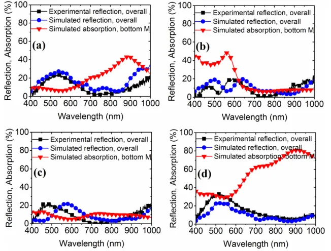
First, we investigate simulation and experimental results of fabricated absorbing MIM structures. Quartz substrate is cleaned by sonicating in acetone and isopropanol which is then rinsed with deionized water. Afterwards, 70 nm absorbing metal has been deposited using thermal evaporator, followed by a 40 nm aluminum oxide deposition in Savannah S100 atomic layer deposition system (ALD). This thickness is optimized in simulations to get high absorption in VIS-NIR region. Finally, the plasmonic layer of nanoparticles has been added as mentioned in the previous section. Fig. 3 depicts normal reflection measurement and reflection simulation with reference to aluminum mirror as well as percentage of absorption in different top metal – aluminum oxide – silver nanoparticles (from bottom to top) structure using Lumerical FDTD between 400 and 1000 nm wavelengths. The simulations are carried out in 3D by importing SEM images into Lumerical FDTD software with a given height of 40 nm for particles estimated from the fill ratio of
Proc. of SPIE Vol. 10099 100991C-2
Downloaded From: https://www.spiedigitallibrary.org/conference-proceedings-of-spie on 12/16/2018 Terms of Use: https://www.spiedigitallibrary.org/terms-of-use
Experimental reflection, overall Simulated reflection, overall Simulated absorption, bottom M
100
ó 80
Experimental reflection, overall Simulated reflection, overall Simulated absorption, bottom M
ó 60
á
40
0
wvi,""vo./
'5 (b) )<
40
c-o
á
20-t
20-a
re-
a)-,,
0 r 0400 500 600 700 800 900 1000
400 500 600 700 800 900 1000
Wavelength (nm) Wavelength (nm):;'100
ô 100
Experimental reflection, overall °\. Experimental reflection, overall
ó 80
Simulated reflection, overall _2- Simulated absorption, bottom M
L
ó 60 (c)
ó 80
Simulated reflection, overall Simulated absorption, bottom ML ó 60
d
2
` )
Q
40
oá
20PrZele%
LT) o1
o400 500 600 700 800 900 1000
400 500 600 700 800 900 1000
Wavelength (nm) Wavelength (nm) (a) (b) (C) (d)particles. The reflection simulation results are consistent with the experimental ones, which opens our path to estimate the amount of absorption in the absorbing metal (bottom metal of absorbing MIM) using simulations. It should be pointed out that since we measure normal reflection and incorporate it into absorption, bottom metal is chosen thick enough to eradicate possibility of transmission. Thus, A = 1 – R [5].
Figure 3. Experimental and simulated reflection, simulated absorption for bottom (absorbing) metal of MIM structures from top to bottom: silver nanoparticles – aluminum oxide - (a) aluminum, (b) gold, (c) silver, (d) chromium absorbing metals.
While there is negligible absorption in silver and gold bottom metal cases in NIR, we observe an absorption peak of 40% at 850 nm and 82% at 980 nm for aluminum and chromium top metals, respectively. Yet, gold is a proper absorber in VIS. The photographs taken from these four samples are illustrated in Fig. 4 which are congruent with their reflection results in Fig. 3.
Figure 4. Sample photos for MIMs of previous figure with (a) al, (b) Au, (c) Ag and (d) Cr absorbing metals.
Proc. of SPIE Vol. 10099 100991C-3
Downloaded From: https://www.spiedigitallibrary.org/conference-proceedings-of-spie on 12/16/2018 Terms of Use: https://www.spiedigitallibrary.org/terms-of-use
A 1,11111) A k11111)
...A.St -
-
-
.I
t Aluminum
- 0-Gold
' -A- Silver
400
660
860
1000
400
á
200
c
03
-200-
(b)
-400-
1-400
660
800
1000
Wavelength (nm)
Wavelength (nm)
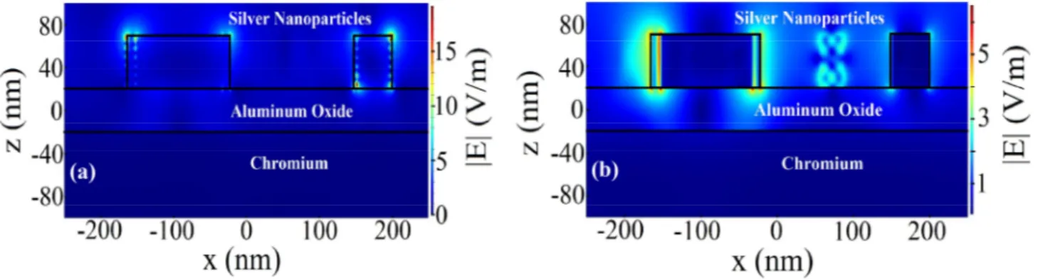
Figs. 5 (a) and (b) illustrate electric field simulations at starting (400 nm) and ending (1000 nm) wavelengths for chromium bottom metal – aluminum oxide – silver nanoparticle structure in a randomly selected cross section with two nanoparticles. The E-field distribution results for other absorbing metal MIMs are analogous with little intensity change.
Figure 5. Electric field simulation in a randomly selected cross section of an MIM device with chromium absorbing metal at (a) 400nm and (b) 1000nm.
At 400 nm, lower order plasmonic mode is excited and fields are mainly confined in silver nanoparticle - air interface resulting in localized surface plasmon resonance excitation in nanoparticles while higher order modes exist at 1000 nm confining light between the silver nanoparticles - aluminum oxide interface giving rise to absorption probability through excitation of surface plasmons in top metal. In order to further vindicate our simulation and reasoning and elucidating on the physics of absorption phenomena we can investigate the loss tangent or quality factor of SPPs for top metals. These methods have been neglected in plasmonic device designs. To the contrary, they shed light on proper choices of metals for each layer. The electric loss tangent is defined as the ratio of the ratio of the imaginary part of the refractive index to the real part of it and it is depicted for four different metals in Fig. 6. We have used Palik [6] model for aluminum, silver and chromium and Johnson and Christy [7] model for gold. The lower the quality factor (or equivalently, the higher the loss tangent) of metal, the higher the absorption.
Figure 6. Electric loss tangent of (a) Al, Au and Ag and (b) Cr.
A metal is considered a good absorber in a wavelength of interest, when it has low real permittivity (to allow light penetration) and high complex permittivity (high absorption), which translates to loss tangent maxima and minima. Aluminum has a relative minimum at 800 nm while the situation is dramatic for chromium; plasma frequency of chromium is at 850 nm (sign change in real part of permittivity) making it an outstanding absorber for NIR wavelengths. It is also obvious from Fig. 6 that Au is a good absorber in VIS region. It can also be deduced from these data that if metals are not absorbing, they are more metallic, meaning that they are capable of scattering light better. Therefore, silver is indeed an accurate choice as plasmonic layer metal, because in this case we want maximum scattering in nanoparticle layer that can excite SPs in absorbing metal. Citing loss tangent and quality factor of SPP as favorable seems counterintuitive due to the fact that the opposite trend is always interesting in most of the designs trying to address
Proc. of SPIE Vol. 10099 100991C-4
Downloaded From: https://www.spiedigitallibrary.org/conference-proceedings-of-spie on 12/16/2018 Terms of Use: https://www.spiedigitallibrary.org/terms-of-use
VD,
pi
(DAat
1
OA
==as==
-0- Cr absorbing metal 1(dark) =7nA
1
Hot e. 0.1
Tr
11
Ë
I
I
LightJ
0.1-50 m
bias
T
r
a
{ i(a) -2.0 -1.5 -1.0 -0.5 0.0 0.5 1.0 1.5 2.00 0
Voltage (V)issues regarding plasmonic waveguides, which obviously require low-loss metals. Since we are interested in non-radiative decay of excited SPPs to generate energetic hot carriers, we are excavating the opposite high-loss property. 2.3 MIMIM photodetector
The best candidate for absorption is extended to form an MIMIM photodetector. MIMIM (from bottom to top, silver - hafnium oxide – chromium top metal – aluminum oxide – silver nanoparticles) device performance with chromium top (absorbing) metal is investigated due to its capability of high absorption. Hafnium oxide is a high-k insulator which is favorable for tunneling junctions. The device consists of silicon substrate, 70 nm bottom metal (negative contact), 4 nm tunneling hafnium oxide, 30 nm middle (absorbing) metal (positive contact), 40 nm aluminum oxide and finally silver nanoparticles. The depositions of metals and dielectrics are carried out using thermal evaporator at 2-5x10⁻⁶ Torr and
atomic layer deposition at 200◦C respectively. The photocollection bias is illustrated in Figs. 1 and 7 (a) and the photocollection phenomenon is depicted in Fig. 7 (a).
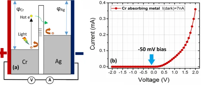
Figure 7. (a) Schematic of photocollection in the bottom MIM junction with chromium absorbing metal (30 nm Cr – 4 nm HfO2 – 70 nm Ag) and (b) Experimental IV characteristics of MIM junction of part (a) with indicated dark current at
-50mV bias.
The reason for choosing 30 nm thick absorbing metal (which is shared between two MIMs) is that the skin depth of metals in the wavelengths of interest are approximately 20 nm and another 10 nm is added to this value as a safety margin in order to block any possible penetration of light through the stack to bottom metal which would result in counteracting reverse photocurrent [8]. This counteracting photocurrent would be as a result of hot-hole generation in bottom metal where a negative bias already exists. It is worth pointing out that further increase in top metal thickness will result in ohmic loss of hot carriers which is highly disadvantageous. Moreover, 4 nm hafnium oxide is an optimum thickness as a compromise between obtaining a continuous film and lower loss of photocurrent.
In order to design effective hot carrier collection junction, we use tunneling method and propose silver as bottom metal. The reason for this selection is that we need a metal with a lower work function than that of chromium, so that we could only collect hot electrons generated in top metal with reverse bias and block the flow of dark current (one can design this junction the opposite way to collect hot holes). This design is successful as can be inferred from the I-V curve in Fig. 7 (b). We have a very low dark current at the negative bias. The device areas are 300 μm × 600 μm. Figs. 8 (a) and (b) represent photoresponsivity of MIMIM devices with and without silver nanoparticles for chromium, measured at a negative bias of 50 mV. Moreover, the simulated absorption in the absorbing metal is provided from Fig. 3 to facilitate comparison.
Gradually increasing the bias, we observe that we get higher photocurrent until we reach 50 mV and any further increase of bias results in the same photocurrent, and only dark current increases. This phenomenon also solidifies the fact that our measured current is photocurrent. Bias is 50 mV for all devices at which we have low dark currents of 7 nA. The photocurrent results are in agreement with the simulated absorption of Fig. 3 (d) as provided in Fig. 8. Even though,
Proc. of SPIE Vol. 10099 100991C-5
Downloaded From: https://www.spiedigitallibrary.org/conference-proceedings-of-spie on 12/16/2018 Terms of Use: https://www.spiedigitallibrary.org/terms-of-use
PR, MIMI device with Cr 80
0.0s
--'> 0.06
PR,MIMIMdevice with Cr
^
-- Simulated absorption in Cr 70ó
pit
60 C
/AL
)\
V50 Q
40 U.ULkipi9r)1,1
ó
0.00
A\&-A-AFA-A-A-A-A4,4,..,._ _cD30 Q
20 a_400
600 800 1000 1200 1400 16'00Wavelength (nm)
there is a red-shift in photoresponsivity compared to absorption results of, which is due to the tarnishing of silver nanoparticles. To justify this statement, the reflection experiments and simulations can be investigated. In Fig. 3 results, there is a blue-shift in experimental reflection compared to those of simulations (reflection trend is the opposite of absorption trend) due to tarnishing of silver nanoparticles that is inevitable in experiments. Thus, the same trend is recognized in photocurrent results.
Figure 8. Photoresponsivity at applied negative 50 mV bias and absorption for MIMI and MIMIM devices with chromium middle (absorbing) metals.
The photoresponsivity of MIMIM device with chromium middle (absorbing) metal exhibits a peak photoresponsivity of 96.24 μA/W at 980 nm which represents 3 times enhancement compared to MIMI device with chromium. Our broadband photocurrent also matches with absorption simulation results. We demonstrate nearly 70 times enhancement compared to former reported spin coated rare nanoparticle MIMIM devices [4].
3. CONCLUSION
We present a photodetector which consist of optimizing different parts of the devices including dewetting, plasmonic top MIM absorption and bottom MIM photocollection junction and put forth the most optimum results. Therefore, we successfully manage to decouple absorption and photocollection sections which facilitates efficient device engineering. We also point out Cr as an excellent metal for NIR plasmonic applications for the first time that is potential for more research. Our best obtained photoresponsivity for MIMIM device with Cr top metal is 96.24 μA/W with a dark current of only 7 nA with 300 μm × 600 μm device areas. Our broadband photocurrent also matches excellently with absorption simulation results. We demonstrate nearly 70 times enhancement compared to former reported spin coated rare nanoparticle MIMIM devices.
ACKNOWLEDGMENTS
This work was partially supported by the Scientific and Technological Research Council of Turkey (TUBITAK), grant nos. 112E052, and 113M815. A.K.O. acknowledges partial support from the Turkish Academy of Sciences Distinguished Young Scientist Award (TUBA GEBIP) and BAGEP and FABED awards.
REFERENCES
[1] Aydin, K., Ferry, V. E., Briggs, R. M., and Atwater, H. A., “Broadband polarization-independent resonant light absorption using ultrathin plasmonic super absorbers,” Nat. Commun. 2, 517 (2011).
[2] Kim, W., Simpkins, B. S., Long, J. P., Zhang, B., Hendrickson, J., and Guo, J., “Localized and nonlocalized plasmon resonance enhanced light absorption in metal-insulator-metal nanostructures,” J. Opt. Soc. Am. B, 32(8), 1686-1692 (2015).
Proc. of SPIE Vol. 10099 100991C-6
Downloaded From: https://www.spiedigitallibrary.org/conference-proceedings-of-spie on 12/16/2018 Terms of Use: https://www.spiedigitallibrary.org/terms-of-use
[3] Wang, F., and Melosh, N. A., “Plasmonic energy collection through hot carrier extraction,” Nano Lett., 11, 5426–5430 (2011).
[4] Atar, F. B., Battal, E., Aygun, L. E., Daglar, B., Bayindir, M., and Okyay, A. K., “Plasmonically enhanced hot electron based photovoltaic device,” Opt. Express, 21(6), 7196-7201 (2013).
[5] Abedini Dereshgi, S., Okyay, A. K., “Large area compatible broadband superabsorber surfaces in the VIS-NIR spectrum utilizing metal-insulator-metal stack and plasmonic nanoparticles,” Opt. Express, 24(16), 17644-17653 (2016).
[6] Palik, E., [Handbook of optical constants of solids], Academic, (1985).
[7] Johnson, P. B., and Christy, R. [Optical constants of the noble metals], Phys. Rev. B 6, 4370 (1972).
[8] Maier, S. A., [Plasmonics: fundamentals and applications], Springer Science & Business Media, 29-30 (2007).
Proc. of SPIE Vol. 10099 100991C-7
Downloaded From: https://www.spiedigitallibrary.org/conference-proceedings-of-spie on 12/16/2018 Terms of Use: https://www.spiedigitallibrary.org/terms-of-use