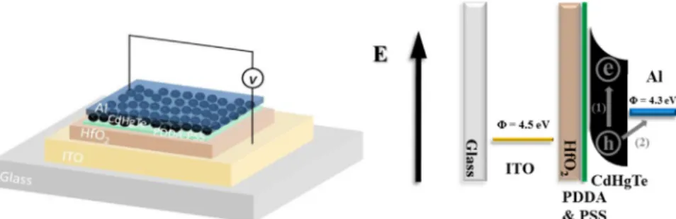
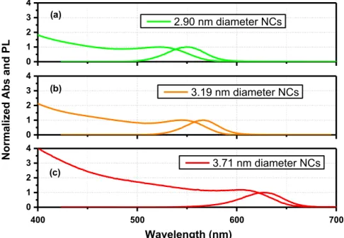
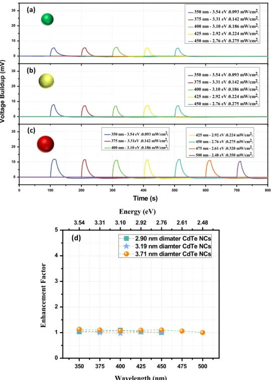
Multiexciton generation assisted highly photosensitive CdHgTe nanocrystal skins
Tam metin
Şekil
Benzer Belgeler
Prior to modeling of miniaturized square patch, the traditional patch is modeled using transmission line model of patch as shown in Figure 17 where the two radiating slots along
(1996): Increased expression of the insulin-like growth factor I (IGF-I) receptor gene in hepatocellular carcinoma cell lines: implications of IGF-I receptor gene activation
For staging of lung cancer, mediastinal lymph nodes were assessed based on the seventh edition of The International Association for the Study of Lung Cancer (IASLC)
C) Verilen kelimelerle aşağıdaki boşlukları doldurunuz.. I can look after
In this study, natural convection over three different geometries; isothermal horizontal duct, vertical plate and an isothermal horizontal flat plate subjected to heat transfer
in investments in the energy sector would not be to have control of the energy sector and to struggle against foreign capital at all; instead, the main objective of the government
1811 tarihli mubayaa hükmünde, zahire mubayaası Teke Mütesellimi Hacı Mehmed Ağa’nın uhdesine havale edildi. Zahire mubayaacısı olarak da İstanbul’dan Abdülfettah
Tedavi bitiminde FREMS ve TENS tedavisi grubundaki hastaların bel ve bacak ağrısı VAS, Oswestry Dizabilite Skoru, Roland-Morris Dizabilite Skoru, lateral fleksiyon ve el parmak-
