COMPUTATIONAL STUDY OF EXCITONS
AND BIEXCITONS IN SEMICONDUCTOR
CORE/SHELL NANOCRYSTALS OF TYPE I
AND TYPE II
a thesis
submitted to the department of physics
and the graduate school of engineering and science
of bilkent university
in partial fulfillment of the requirements
for the degree of
master of science
By
Ozan Yerli
ABSTRACT
COMPUTATIONAL STUDY OF EXCITONS AND
BIEXCITONS IN SEMICONDUCTOR CORE/SHELL
NANOCRYSTALS OF TYPE I AND TYPE II
Ozan Yerli M.S. in Physics
Supervisor: Assoc. Prof. Hilmi Volkan Demir July, 2013
In this thesis, we studied electronic structure and optical properties of Type-I, Type-II, and quasi Type-II semiconductor nanocrystals (also known as colloidal quantum dots). For a parametric study, we developed quantum mechanical mod-els and solved them using both analytical and numerical techniques. The simula-tion results were compared to the experimental findings. We showed that charge carrier localization at di↵erent spatial locations could be tuned by controlling size parameters of the core and shell.
While tuning charge localization, we also predicted photoluminescence peaks of these core/shell nanocrystals using our theoretical and numerical calculations. We demonstrated that Type-II nanocrystals exhibit di↵erent tuning trends com-pared to the Type-I ones.
We also investigated biexcitonic properties of nanocrystals using quantum mechanical simulations, which are important especially in lasing applications. We showed that two-photon absorption mechanism can be tuned by changing the core and shell size in quantum dots. We calculated at which core and shell sizes biexcitons in quantum dots show attractive or repulsive interaction. The computational studies presented in this thesis played an important role in the experimental demonstrations and understanding of controlling excitonic features of core/shell nanocrystals.
Keywords: Nanocrystals, quantum dots, two photon absorption, exciton, biexci-ton, amplified spontaneous emission.
¨
OZET
YARI ˙ILETKEN T˙IP I VE T˙IP II C
¸ EKIRDEK/KABUK
NANOKR˙ISTALLERDEK˙I EKS˙ITON VE
B˙IEKS˙ITONLARIN HESAPLAMALI ˙INCELEMES˙I
Ozan Yerli Fizik, Y¨uksek Lisans
Tez Y¨oneticisi: Do¸c. Dr. Hilmi Volkan Demir Temmuz 2013
Bu tezde, Tip-I, Tip-II ve Tip-II benzeri kuantum nokta nanokristallerin elek-tronik ve optik ¨ozelliklerini inceledik. Parametrik bir ¸calı¸sma i¸cin kuan-tum mekaniksel modeller geli¸stirildi, analitik ve numerik teknikler kullanılarak ¸c¨oz¨uld¨u. Simulasyon sonu¸cları deneysel sonu¸clarla kar¸sıla¸stırıldı. Y¨uk ta¸sıyıcıların farklı b¨olgelerdeki lokalizasyonunun ¸cekirdek ve kabuk yapılarının boyutlarını de˘gi¸stirerek ayarlanabilece˘gi g¨osterildi.
Y¨uk lokalizasyonunun ayarlanmasının yanında, ¸cekirdek/kabuk nanokristal-lerinin ı¸sıma tepe noktaları teorik ve numerik hesaplarla ¨ong¨or¨uld¨u. Ayrıca Tip-II nanokristallerin Tip-I nanokristallere g¨ore farklı ayar e˘gilimlerine sahip oldukları g¨osterildi.
Kuantum mekaniksel simulasyonları kullanarak nanokristallerin ¨ozellikle lazer uygulamalarında olduk¸ca ¨onemli olan bieksitonik ¨ozellikleri incelendi. ˙Iki fo-ton so˘gurma mekanizmasının kuantum noktaların ¸cekirdek ve kabuk boyutlarıyla ayarlanabilece˘gini g¨osterdik. Hangi ¸cekirdek ve kabuk boyutlarında bieksiton-ların ¸cekici veya itici etkile¸sim g¨osterdiklerini hesapladık. Bu tezde sunulan hesaplamalı ara¸stırmalar ¸cekirdek/kabuk nanokristallerin eksitonik ¨ozelliklerinin kontrol¨un¨un anla¸sılmasında ve deneysel olarak g¨osterilmesinde ¨onemli bir rol oy-namı¸stır.
Anahtar s¨ozc¨ukler : Nanokristaller, kuantum noktaları, iki foton so˘gurması, eksi-ton, bieksieksi-ton, artırılmı¸s kendili˘ginden ı¸sıma.
Acknowledgement
I would like to thank Assoc. Prof. Hilmi Volkan Demir for his invaluable support, suggestions, and guidance during my studies.
I would like to acknowledge Prof. O˘guz G¨ulseren and Assoc. Prof. Vakur B. Ert¨urk for reading the thesis and being in the thesis committee.
I would like to thank all my instructors and members of the Physics Depart-ment for helping me get a strong understanding of physics.
I would like to acknowledge Ahmet Fatih Cihan, Yusuf Kelestemur, and Burak Guzelturk for their valuable discussions about topics in this thesis. I also thank them for helping me to get the experimental results which I used to compare with my computational results in this thesis.
I would like to thank Kıvan¸c G¨ung¨or, Shahab Akhavan, Talha Erdem, Aydan Yeltik, Can Uran, and all other HVD Group members for their support and help during my master’s studies.
I would like to thank my colleagues, ˙Ismail Can O˘guz and Kutan G¨urel for making this 2 year of studies delightful and productive.
I would like to thank Elif Yıldız, Enis D¨onmez, Yurdakul G¨oksu Orhun for their moral support during this intensive period of mine.
I would like to thank Almıla for being in my life. She gave extensive support and motivation which helped me complete this thesis.
I would like acknowledge my family, my mother Hilal, my father Nusret, and my grandmother Y¨uksel. Without their help, support and love I would not be successful.
Contents
1 INTRODUCTION 1 2 NANOCRYSTAL OPTOELECTRONICS 5 2.1 Introduction . . . 5 2.2 Theoretical Model . . . 6 2.3 Optical Properties . . . 7 2.4 Classification of Nanocrystals . . . 8 2.4.1 Type-I . . . 8 2.4.2 Type-II . . . 93 QUANTUM MECHANICAL SIMULATIONS 11 3.1 Introduction . . . 11
3.2 Atomic Unit System . . . 12
3.3 E↵ective Mass Approximation . . . 12
3.4 Single Particle Simulations . . . 13
CONTENTS vii
3.6 Material Parameters . . . 16
4 MULTIGRID TECHNIQUE 17 4.1 Introduction . . . 17
4.2 Kronecker Tensor Product . . . 19
4.3 Poisson’s Equation in 1D . . . 19
4.4 Standard Ordering . . . 20
4.5 Poisson’s Equation in 2D and 3D . . . 21
4.6 Multigrid Algorithm . . . 21
5 RESULTS AND DISCUSSION 28 5.1 Electron and Hole Wavefunctions and Energies for Type I/Type II Spherical QDs . . . 28
5.2 Oscillator Strength of Excitons Confined in Type I/Type II Spher-ical QDs . . . 32
5.3 Biexciton Binding Energies for Type I/Type II Spherical QDs . . 34
6 CONCLUSION 40
List of Figures
1.1 Nanocrystals of di↵erent sizes illuminated with ultraviolet light after [2]. . . 2 1.2 Band structure of the CdTe/CdSe core-shell Type-II nanocrystal. 3
2.1 Schematic and potential diagram of a Type-I nanocrystal (CdSe / ZnS) after [28]. . . 10 2.2 Schematic and potential diagram of a Type-II nanocrystal (CdTe
/ CdSe) after [28]. . . 10
4.1 Multigrid schema after [41]. . . 18 4.2 Charge distribution of a single electron in the state (1,1,1) of a
quantum dot. . . 24 4.3 Potential of a single electron in the state (1,1,1) of a quantum dot. 24 4.4 Isopotential surface slice of a single electron in the state (1,1,1) of
a quantum dot. . . 25 4.5 Charge distribution of a single electron in the state (2,1,1) of a
quantum dot. . . 26 4.6 Potential of a single electron in the state (2,1,1) of a quantum dot. 26
LIST OF FIGURES ix
4.7 Isopotential surface slice of a single electron in the state (2,1,1) of a quantum dot. . . 27
5.1 Wavefunctions of electron and hole for CdSe/ZnS (Type-I) 1s-state. 29 5.2 Exciton energy of CdSe/ZnS (Type-I) with respect to d1 for
dif-ferent shell thicknesses. . . 30 5.3 Wavefunctions of electron and hole for CdTe/CdSe (Type-II)
1s-state with parameters d1 = 22A, d2 = 33A. . . 30
5.4 Wavefunctions of electron and hole for CdTe/CdSe (Type-II) 1s-state with parameters d1 = 22A, d2 = 25A. . . 31
5.5 Exciton energy of CdTe/CdSe (Type-II) with respect to d1 for
di↵erent shell thicknesses. . . 31 5.6 Oscillator strength of CdSe/ZnS (Type-I) with respect to d1 for
di↵erent shell thicknesses. . . 33 5.7 Oscillator strength of CdTe/CdSe (Type-II) with respect to d1 for
di↵erent shell thicknesses. . . 33 5.8 Schematics of the quantum dots synthesized. . . 35 5.9 ASE peak shift with respect to spontaneous emission for di↵erent
core/shell sizes of CdSe/CdS core/shell quantum dots. . . 36 5.10 Experimental ASE spectra of the quantum dots synthesized. . . . 37 5.11 Simulation results for ASE spectra of the quantum dots synthesized. 38 5.12 The calculated wavefunctions of electrons and holes for CQD1. . . 38
List of Tables
Chapter 1
INTRODUCTION
Semiconductor nanocrystals, or colloidal quantum dots, find many important applications including photovoltaics, lasers, and light-emitting diodes. They are subject of particular interest due to size dependence of their optical properties arising from quantum confinement e↵ects. This size dependence enables us to tune the optoelectronic properties of nanocrystals [1].
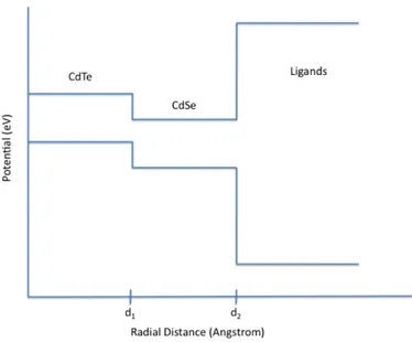
The materials used in nanocrystal heterostructures give rise to di↵erent spatial localization configurations for the electrons and holes in the semiconductor. If the bandgap of one material lies within the bandgap of the other material, the electrons and holes will be found at the same spatial location. This type of band alignment is called Type-I. If both of the bandgaps of the materials have non-overlapping energies, the electrons and holes will localize at the di↵erent spatial positions. This type of band alignment is called Type-II, which can be seen in Figure 1.2.
Figure 1.1: Nanocrystals of di↵erent sizes illuminated with ultraviolet light after [2].
In the Type-II band alignment we can control confinement locations of the charge carriers, which change their wavefunction overlap. We can localize one charge carrier into the core while the other carrier is delocalized over both core and shell. This opens up new possibilities for the usage of nanocrystals including low threshold lasers, fast optical switches, quantum information processors, infrared detectors, and fast access memories [3]. Since these devices require an accurate control on the optoelectronic properties, Type-II nanocrystals may o↵er flexibility. Type-II nanocrystals also have increased emission lifetimes [3].
It is shown that characteristics of Type-I nanocrystals can be obtained from theoretical and numerical calculations with a high degree of accuracy [1]. In order to understand optoelectronic properties of nanocrystals, understanding ex-citonic behaviour is crucial. Various simulation methods and techniques have been developed to investigate excitons in nanocrystals [4] [5] [6] [7] [8] [9].
In this study, we will analytically understand properties of the Type-II het-erostructures and use these to deduce photoluminescence peak of the nanocrys-tals. We will also examine the parameter dependence of the wavefunction localiza-tions and overlap of the electron/hole wavefunclocaliza-tions using numerical techniques.
Figure 1.2: Band structure of the CdTe/CdSe core-shell Type-II nanocrystal. This will allow us to optimize wavefunctions for the desired optoelectronic prop-erties.
Nanocrystals are also suitable for optical gain and lasing applications. Two-photon absorption mechanism has also been shown as a promising method for excitation of optical gain media. In this thesis, using quantum mechanical sim-ulations we show that the single material system of CdSe/CdS can be tuned to give blue or red-shifting behaviour of amplified spontaneous emission (ASE) in two-photon absorption mechanism. This is due to the exciton-exciton interac-tions becoming either attractive or repulsive by tuning the core and shell size. Here using quantum mechanical simulation techniques biexcitonic properties of nanocrystals are investigated.
The organization of the thesis is as follows. In the second chapter we introduce the basics of nanocrystal optoelectronics. We give brief background information on how to model nanocrystals theoretically and their optical properties. In the third chapter we introduce simulation techniques used for solving quantum me-chanical problems. E↵ective mass approximation and self-consistent solution of
multi-particle Schrodinger equations, which are the techniques we used for exci-ton and biexciexci-ton calculations in nanocrystals are explained in this chapter. In the fourth chapter multigrid technique is explained. We used multigrid technique to solve Poisson equation arising from Kohn-Sham equations. In the fifth chapter we present our research work on excitonic and biexcitonic properties of nanocrys-tals. Experimental and simulation results are given in this chapter. In the last chapter, we conclude by providing a summary of our findings and a comparative description of exciton and biexciton properties in di↵erent kinds of nanocrystals.
Chapter 2
NANOCRYSTAL
OPTOELECTRONICS
2.1
Introduction
Nanocrystal quantum dots are nanometer-sized, nearly spherical crystal struc-tures. Since the size of a nanocrystal is comparable with the Bohr radius of excitons in the nanocrystal, the nanocrystal size can a↵ect many properties of the excitons. Using various synthesis techniques the size of nanocrystals can be controlled. This allows us to tune excitonic properties of the nanocrystals very precisely. Due to their tunability, nanocrystal quantum dots are suitable for light-emitting diodes [10], [11], [12] and for lasing applications [13].
Beside tunability of their optoelectronic properties by controlling their size, it is also possible to engineer their shape (spherical, nanorod [14], and tetrapod [15]). Di↵erent shapes also allow for new possibilities for engineering distinct optoelectronic properties.
2.2
Theoretical Model
A spherically symmetric nanocrystal model is used as the theoretical model for the colloidal quantum dots here. As we investigate s-states (l=0 and m=0), the energy level only depends on the radial part of wavefunction, R(r). For s-states, radial part of the Schrodinger equation is:
⇢ 1 2m⇤r2 d dr ✓ r2 d dr ◆ + V (r) R(r) = ER(r) (2.1)
By making u(r) = rR(r) transformation, we can convert the problem into an one-dimensional square potential problem. After the transformation the radial Schrodinger equation becomes:
[ 1
2m⇤
@2
@r2 + V (r)]u(r) = Eu(r) (2.2)
Here we assume the core has radius of d1, and the shell has thickness of
(d2 d1). If we impose boundary conditions at the interface (r = d1), from the
continuity of the wavefunction, we obtain the condition:
uI(d1) = uII(d1) (2.3)
From the continuity of the probability currents, we get the condition [16]: 1 m1 @uI @r d1 = 1 m2 @uII @r d1 (2.4)
In Equations 2.3 and 2.4, uI and uII are the wavefunctions in the regions
0 < r < d1 and d1 < r < d2, respectively. In Equation 2.4, the m1 and m2 are the
e↵ective masses of the charge carriers in di↵erent semiconductors. These material parameters are taken from Table I of the reference [17].
Note that, in Equation 2.4 the first order derivatives of the wavefunction are not continuous because of the e↵ective mass mismatch across the two materials.
The discontinuity of the first order derivatives in di↵erent materials are propor-tional to the ratio of the e↵ective masses in these di↵erent materials. This is known as the BenDaniel-Duke boundary conditions [16].
Applying these boundary conditions, we obtain the following matrix, which should have zero determinant in order to have non-trivial solutions:
A = " e d1k1 + ed1k1 sin(d 1k1) + cos(d1k2)tan(d2k2) k1 m1(e d1k1 + ed1k1) k2
m2[cos(d1k2) + sin(d1k2)tan(d2k2)]
#
(2.5)
We calculated the determinant of the matrix analytically and using Mathe-matica found the solutions for the equation:
detA = 0 (2.6)
We calculated maximum photoluminescence (PL) should occur at 802.4 nm wavelength for a CdTe/CdSe nanocrystal heterostructure with d1 = 32˚A and d2 =
43˚A. These values are lower than the photoluminescence peak of the experimental result in Figure 2 of the reference [18]. Since we assumed an infinite barrier at the ligand interface, we increase the quantum confinement e↵ect, which leads to higher energy elevels. That is the reason why we obtain blue-shifted results for the PL peak compared to the experimental results.
In order to obtain more accurate results for the PL peak calculations, we need to assign a finite potential value to the ligand interface of the heterostructure. In order to solve this problem analytically we need to increase the dimension of the matrix in Equation 2.5. Also, we intend to investigate multi-particle quantum dot systems, which is not possible with the pure analytical model. To address these problems we used numerical techniques that are more efficient than the analytical approach.
2.3
Optical Properties
Since nanocrystals have size comparable to the excitonic Bohr radius, their op-tical properies are di↵ent from the bulk materials. Their opop-tical properties can
be controlled by changing their size. This gives tunability to the emission and absorption spectra of nanocrystals.
There is a shift between the absorption and emission peaks of nanocrystals. Since this shift suppresses reabsorption, it increases luminiscence. In order to further enhance luminiscence, core/shell quantum structures are used. The shell structure passivates the surface and decreases the nonradiative recombination.
Quantum dots are also a good candidate for a gain medium due to their relatively low optical gain thresholds, temperature stability, and narrow emission bandwidth [19]. Using various photonic structures, quantum dot lasers using optical pumping have been developed [20] [21] [22] [23]. However, in these studies single-photon absorption mechanism has been used for optical pumping. As an alternative to single-photon absorption, two-photon absorption (TPA) mechanism can be used. TPA has an advantage of reducing the risk of photo-damaging [24] [25] [26] [27].
As a result of TPA mechanism, two excitons are created. Since two exci-tons are created, the resulting amplified spontaneous emission due to decay of these excitons are related to the biexciton binding energy. Hence, it is important to investigate biexciton energy using simulations in order to create structures optimized for TPA.
2.4
Classification of Nanocrystals
2.4.1
Type-I
In Type-I nanocrystals, the minimum energy region of electrons and holes coin-cide. This causes electrons and holes localize very closely at the same location. A sample potential diagram for a Type-I nanocrystal can be seen in figure 2.1
2.4.2
Type-II
In Type-II nanocrystals, the minimum energy region of electrons is di↵erent from the minimum energy region of holes. For this reason, electrons and holes localize in di↵erent spatial regions. A sample potential diagram for a Type-II nanocrystal can be seen in Figure 2.2.
Type-II nanocrystals have increased optical gain lifetime compared to Type-I nanocrystals because in Type-II nanocrystals Auger recombination is suppressed due to electrons and holes being seperated in di↵erent regions [29], [30].
Figure 2.1: Schematic and potential diagram of a Type-I nanocrystal (CdSe / ZnS) after [28].
Figure 2.2: Schematic and potential diagram of a Type-II nanocrystal (CdTe / CdSe) after [28].
Chapter 3
QUANTUM MECHANICAL
SIMULATIONS
3.1
Introduction
Embedded semiconductor quantum dots have been investigated by Laheld and co-workers theoretically [31]. They used e↵ective-mass approximation and finite-band o↵set between two materials. An average dielectric constant is assumed between both materials. They showed Type-I, Type-II and quasi Type-II prop-erties theoretically.
Colloidal core/shell quantum dots have been investigated using similar tech-niques [32] [33] [34] [35]. The main di↵erence comes from the fact that the outer-most semiconductor is not infinite, it has a finite thickness. This causes electrons and holes to localize in the shell structure. Klimov and co-workers have used e↵ective mass approximation and perturbation theory, which includes interface polarization e↵ects to investigate colloidal quantum dots [35]. Colloidal quantum dots have also been modeled using k.p method, tight-binding, and pseudopoten-tial methods [36] [32].
3.2
Atomic Unit System
In order to make simulations simpler we used the atomic unit system in our calculations. In the atomic unit system ¯h = me= e = 1, where me is the mass of
the electron and e is the charge of the electron [37].
Lengths are expressed in the units of classical Bohr radius which is a0 =
9.5292˚A.
One atomic unit of energy is 27.2116 eV, which is used to convert calculated energies to eV.
3.3
E↵ective Mass Approximation
Group velocity of a free electron wave packet is given by: v = dw
dk (3.1)
We also have the relation between the frequency and the energy: w = E
¯h (3.2)
Hence, the group velocity can be expressed as: v = 1
¯h dE
dk (3.3)
Since the momentum of electron is ¯hk, if we take its derivative, we can write it in the form of Newton’s second law:
dp dt = ¯h dk dt = m ⇤dv dt (3.4)
In Equation 3.4, m⇤ is called the e↵ective mass. If we use the expression for
the group velocity given in Equation 3.3, we obtain the relation: ¯hdk = m⇤1d
2Edk
dk
dt cancels from both sides and we finally arrive at:
1 m⇤ = 1 ¯h2 d2E dk2 (3.6)
Equation 3.6 gives the definition of the e↵ective mass [38]. It shows that in crystalline solids we can calculate e↵ective mass from the dispersion relation. Once we obtain the e↵ective mass we can reduce the problem into a free electron problem. The electron moves in the solid as if it was a free electron with the mass m⇤.
3.4
Single Particle Simulations
In our computational study we first made the transformation u(r) = rR(r) in order to convert the problem into an one-dimensional Schrodinger equation prob-lem. After that transformation and using the atomic units, we need to solve the equation:
[ 1
2m⇤
@2
@r2 + V (r)]u(r) = Eu(r) (3.7)
In Equation 3.7, m⇤ is the ratio of the e↵ective mass of the particle to the free electron mass.
In order to solve this one-dimensional system numerically, we need to discretise radial space, Hamiltonian operator, and wavefunction [39]. We used h = 0.01 as our discretization parameter and meshed the space into equally separated discrete parts, which are h˚A apart.
We can write the second order derivative operator as a finite di↵erence: f00(x) = f (x + h) 2f (x) + f (x h)
h2 (3.8)
Assume we try to solve the following eigenvalue equation: @2
For each point in our discretized space, we can write the Equation 3.8. Hence we obtain the following set of equations (assuming the boundary conditions, f (x0 h) = 0 and f (xn+ h) = 0): 8 > > > > > > > > > > < > > > > > > > > > > : 1 h2[ 2f (x0) + f (x0 + h)] = Ef (x0) 1 h2[f (x1 h) 2f (x1) + f (x1+ h)] = Ef (x1) 1 h2[f (x2 h) 2f (x2) + f (x2+ h)] = Ef (x2) ... 1 h2[f (x2 h) 2f (x2)] = Ef (xn) (3.10)
We can write these set of equations as a matrix equation:
1 h2 2 6 6 6 6 6 6 6 4 2 1 0 · · · 0 1 2 1 · · · 0 0 1 2 1 · · · ... ... ... ... ... 0 0 · · · 1 2 3 7 7 7 7 7 7 7 5 2 6 6 6 6 6 6 6 4 f (x0) f (x1) f (x2) · · · f (xn) 3 7 7 7 7 7 7 7 5 = E 2 6 6 6 6 6 6 6 4 f (x0) f (x1) f (x2) · · · f (xn) 3 7 7 7 7 7 7 7 5 (3.11)
If we solve the matrix equation in Equation 3.11, we obtain values of the eigenfunction f (x) at our discretized space points (x0, x1, x2, ..., xn).
For n space points, the matrix in Equation 3.11 becomes an n-by-n tridiagonal matrix.
Hence, the Hamiltonian operator can be written as a matrix. For example, for three space points, the Hamiltonian operator can be expressed as:
H = 1 2h2 2 6 6 4 2/m⇤1 1/m⇤2 0 1/m⇤ 1 2/m⇤2 1/m⇤3 0 1/m⇤ 2 2/m⇤3 3 7 7 5 + 2 6 6 4 V1 0 0 0 V2 0 0 0 V3 3 7 7 5 (3.12) In Equation 3.12, m⇤
1, m⇤2, and m⇤3 are the e↵ective masses of the particle
and V1, V2, and V3 are the potential energies in the space points 1, 2, and 3,
By writing the Hamiltonian of the system using finite di↵erence method and finding its eigenvectors using computational techniques, we can obtain energies and wavefunctions of single particles.
3.5
Multi-Particle Simulations
For a multi-particle system, we can write the following set of Schrodinger
equa-tions [40]: ✓ ¯h2 2m⇤r 2+ V ef f(~r) ◆ i(~r) = ✏i i(~r) (3.13)
where ¯h is the reduced Planck constant, m⇤ is the e↵ective electron (or hole)
mass, Vef f is the e↵ective potential, i is the wavefunction of the ith electron (or
hole), ✏i is the energy of the ith electron (or hole).
Here we use e↵ective mass approximation to calculate the energy eigenvalue and wavefunction of the first electron. Then we calculate the charge density using the equation: ⇢(~r) = N X i | i(~r)|2 (3.14)
where N is the total number of charge carriers.
We use the charge density in our multigrid Poisson equation solver to calculate the new e↵ective potential:
r2Vef f =
⇢
✏ (3.15)
Using this new e↵ective potential we repeat the calculations including the first hole, the second electron, and the second hole until we obtain a self-consistent set of charge densities and wavefunctions.
3.6
Material Parameters
The material parameters for CdSe/CdS quantum dots used in this thesis are taken from the supplementary information of the reference [19]:
Parameter CdSe CdS
Electron E↵ective Mass 0.13 m0 0.21 m0
Hole E↵ective Mass 0.45 m0 0.68 m0
Bandgap Energy 1.75 eV 2.50 eV
Table 3.1: Material parameters for CdSe/CdS quantum dots.
For the CdSe/ZnS Type-I core/shell structure, for electrons, we assigned zero potential energy inside the CdSe core and used a barrier of 1.05 eV for the ZnS shell. The ligand barrier for the electrons is 4 eV. For holes, we assigned zero potential energy inside the CdSe core and used a barrier of 0.95 eV for the ZnS shell. The ligand barrier for the holes is 10 eV.
For the CdTe/CdSe Type-II core/shell structure, for electrons, we again as-signed zero potential energy inside the CdSe shell and used a barrier of 0.67 eV for the CdTe core. The ligand barrier for the electrons is 4 eV. For holes, we used zero potential energy inside the CdTe core and took a barrier of 0.97 eV for the CdSe shell. The ligand barrier for the holes is 10 eV.
Chapter 4
MULTIGRID TECHNIQUE
4.1
Introduction
In 1D, Poisson’s equation can be easily solved by writing Laplacian operator as a matrix, and since we already have our potential and charge density vectors as 1D vectors, we can write the system in the form of Ax = b, and solve it either directly by taking inverse or using iterative methods (Jacobi, Gauss-Seidel, Successive Over-Relaxation, Multigrid) [41].
In higher dimensions, since we still have a linear operator (Laplacian), we can still write the problem as a linear algebra problem but this time the matrix A and b are not self-evident. We need to develop a technique to map n⇥ n ⇥ n 3D arrays of potential and charge density into column vectors.
Figure 4.1: Multigrid schema after [41].
Matrix representation of the Laplacian operator in 3D has very large dimen-sions. Using standard techniques it takes a large amount of time to solve this matrix system. Using the multigrid technique we can solve very large matrix systems efficiently. In the multigrid technique using the restriction operator we map the system into a coarser grid which can be seen in Figure 4.1. Then in this new grid, we recursively call our multigrid procedure. In the coarsest grid, we solve the problem directly. After we solve the problem in the coarsest grid, we interpolate the solution back into to the original grid. This operation takes less time compared to the direct solution of the original problem [41].
In this thesis, we used Kronecker tensor product to create 2D and 3D Lapla-cian matrices and interpolation/restriction matrices for the multigrid technique. We created these matrices from their analogous 1D matrices. We obtain the po-tential and solution vectors using the technique “standard ordering”, which will be explained later.
4.2
Kronecker Tensor Product
The Kronecker tensor product of two matrices creates a higher dimensional block matrix in the following way [42]:
Let A be an m⇥ n matrix and B be a p ⇥ q matrix. Their Kronecker tensor product is an mp⇥ nq matrix given by:
A⌦ B = 2 6 6 4 a11B · · · a1nB ... . .. ... am1B · · · amnB 3 7 7 5 (4.1)
We write the matrix B, by multiplying with elements of A and obtain a large block matrix.
4.3
Poisson’s Equation in 1D
Poisson’s equation in 1D can be expressed in the matrix form by using the second order finite di↵erence formula. The result is (for 3 points in 1D):
2 6 6 4 2 1 0 1 2 1 0 1 2 3 7 7 5 2 6 6 4 x1 x2 x3 3 7 7 5 = 2 6 6 4 b1 b2 b3 3 7 7 5 (4.2)
In this point of view, we can easily see the averaging property of the Laplacian operator. Here, b1, b2, b3 are the charge densities divided by the permittivity in
the corresponding points. If we want to add the boundary conditions, we add the potential at the two boundaries to b1 and b3. Hence, this matrix system fully
4.4
Standard Ordering
Let M be an m⇥ m ⇥ m 3D array in MATLAB, then the command v=M(:) gives a vector that has formed by applying standard ordering to the array M. In the graphical representation, the vector v is created in this way:
2 6 6 6 6 6 6 6 6 6 6 6 6 6 6 6 6 6 6 6 6 6 6 6 6 6 6 6 6 6 6 6 6 6 6 6 6 6 6 6 6 6 6 6 6 6 6 4 M (1, 1, 1) M (2, 1, 1) M (3, 1, 1) ... ... M (1, 2, 1) M (2, 2, 1) ... ... M (1, 3, 1) M (2, 3, 1) ... ... ... M (1, 1, 3) M (2, 1, 3) ... ... ... M (3, 3, 3) 3 7 7 7 7 7 7 7 7 7 7 7 7 7 7 7 7 7 7 7 7 7 7 7 7 7 7 7 7 7 7 7 7 7 7 7 7 7 7 7 7 7 7 7 7 7 7 5 (4.3)
So this vector has exactly m3 elements, created by first iterating the first
4.5
Poisson’s Equation in 2D and 3D
If we use standard ordering in our vectors, x and b, the corresponding Laplacian matrices can be easily obtained by the Kronecker tensor product [42].
A2D= A1D⌦ I1D+ I1D⌦ A1D (4.4)
A3D= A2D⌦ I2D+ I2D⌦ A2D (4.5)
As expected in 2D we obtain a matrix that averages 4 points neighboring the middle point. In 3D matrix we have 6 points between the middle point averaged. So, the problem in 3D is reduced into a sparse linear system solution, which is very convenient, since we can use all techniques developed for linear algebra, and even we can solve the matrix system exactly (by spending a lot of time).
Here we used the solution obtained using MATLAB’s sparse matrix solver sub-routines to find the optimal values for multigrid pre-smoothing/post-smoothing parameters.
4.6
Multigrid Algorithm
In order to implement the multigrid method, we need two new matrices: re-striction and interpolation. The rere-striction matrix takes a vector from a finer grid and maps it into a vector in a coarser grid. The interpolation grid does the vice-versa. Since the dimension of linear space changes, the restriction and interpolation matrices are rectangular.
for n=7 we can write the restriction matrix as: R1D = 2 6 6 4 1/4 1/2 1/4 0 0 0 0 0 0 1/4 1/2 1/4 0 0 0 0 0 0 1/4 1/2 1/4 3 7 7 5 (4.6)
As we can see, R1D takes weighted averages of the neighboring points and
writes them into the coarser grid. The interpolation operator in 1D is just the transpose of R1D multiplied by 2 (to ensure normalization).
We can obtain the restriction and interpolation matrices for 2D and 3D using the Kronecker Tensor Product:
R2D = R1D⌦ R1D (4.7)
R3D = R2D⌦ R1D (4.8)
Once we have the restriction and interpolation matrices at hand, we can use the multigrid algorithm as follows [41]:
1. Make an initial guess for the solution: xh
2. Calculate the residual: rh = bh Axh
3. Restrict the residual to a coarser grid: r2h= Rrh
4. “Solve” the system A2hE2h= r2hand get a correction term (E2h). Here, A2h
is obtained from the formula: A2h= RAI (It is equivalent to interpolating
a vector, applying A to it, and then restricting it back.) In this step, for “solving” this new system, we again recursively call our multigrid procedure to solve it again using the multigrid. In the coarsest level, we solve the system directly. If we iterate this step more than once, we get W-cycle and Full Multigrid.
5. Interpolate back the correction term Eh = IE2h and add the interpolated
6. Using the new approximate solution return to step 1. If the residual becomes “negligible” (in our case ⇠ 10 5), terminate iteration.
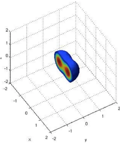
In Figures 4.2, 4.3, 4.4, 4.5, 4.6, 4.7 we present some sample results of our multigrid Poisson solver.
Figure 4.2: Charge distribution of a single electron in the state (1,1,1) of a quan-tum dot.
Figure 4.4: Isopotential surface slice of a single electron in the state (1,1,1) of a quantum dot.
Figure 4.5: Charge distribution of a single electron in the state (2,1,1) of a quan-tum dot.
Figure 4.7: Isopotential surface slice of a single electron in the state (2,1,1) of a quantum dot.
Chapter 5
RESULTS AND DISCUSSION
5.1
Electron and Hole Wavefunctions and
En-ergies for Type I/Type II Spherical QDs
As observed in Figure 5.2 exciton energy decreases by increasing core radius since this decreases the quantum confinement e↵ect. The increasing shell thickness slightly decrease energy for small cores but does not alter the energy very much. This can be understood when we look at the wavefunction distribution in Figure 5.1. Since both wavefunctions are mostly confined to the core, varying the shell thickness does not a↵ect the exciton energy much.
We calculated that the wavefunctions of electron and hole can be localized at di↵erent spatial locations in Type-II heterostructures as seen in Figure 5.3. Also, by changing the shell thickness, we can confine the electron and hole to the same spatial location as observed in Figure 5.4. This shows that Type-II heterostructures give us more control on the charge carrier localizations.
When we consider the PL peak energies of di↵erent Type-II structures, we observe that both the core and shell size a↵ect the exciton energy since one of the charge carrier is confined in the core while the other in the shell. This leads to separated energy curves presented in Figure 5.5. These curves coincide when
Figure 5.1: Wavefunctions of electron and hole for CdSe/ZnS (Type-I) 1s-state. the structure is Type I as observed in Figure 5.2.
Figure 5.2: Exciton energy of CdSe/ZnS (Type-I) with respect to d1 for di↵erent
shell thicknesses.
Figure 5.3: Wavefunctions of electron and hole for CdTe/CdSe (Type-II) 1s-state with parameters d1 = 22A, d2 = 33A.
Figure 5.4: Wavefunctions of electron and hole for CdTe/CdSe (Type-II) 1s-state with parameters d1 = 22A, d2 = 25A.
Figure 5.5: Exciton energy of CdTe/CdSe (Type-II) with respect to d1 for
5.2
Oscillator Strength of Excitons Confined in
Type I/Type II Spherical QDs
Oscillator strength is proportional to the interaction strength of the quantum dot with the external electromagnetic field. It is very important to have a high os-cillator strength for the applications that utilize spontaneous emission. In cavity applications, oscillator strength determines the strength of interaction between the cavity field and the quantum dot [43].
In theoretical calculations, the oscillator strength is proportional to the over-lap integral of the charge carriers [44]:
f = Ep 2Eexc |
Z
d3r e(r) h(r)|2 (5.1)
where Ep is the Kane energy; Eexc is the exciton energy; e and h are the
wavefunctions of the electron and hole, respectively.
The oscillator strength of the Type-I heterostructure increases with increasing core radius for all shell thicknesses as we see in Figure 5.6. However, in the Type-II heterostructure, when the shell thickness is high, increasing the core radius decreases the oscillator strength. For small shell thicknesses of Type-II structure, increasing the core radius increases the oscillator strength. These di↵erent regimes can be seen in Figure 5.7. This can be explained by the above discussion that small shell thicknesses cause electron and hole to localize in the same spatial location like in the Type-I structure. That is why the oscillator strength behaves as in the Type-I structure for small shell thicknesses of the Type-II structure.
Figure 5.6: Oscillator strength of CdSe/ZnS (Type-I) with respect to d1 for
dif-ferent shell thicknesses.
Figure 5.7: Oscillator strength of CdTe/CdSe (Type-II) with respect to d1 for
5.3
Biexciton Binding Energies for Type
I/-Type II Spherical QDs
Since electron and hole energies of the second exciton are higher than the first exciton, if exciton-exciton interaction is not strong, amplified spontaneous emis-sion peak (i.e., energy of the second exciton in the biexction) will be blue-shifted with respect to the spontaneous emission peak (i.e., energy of a single exciton).
Since exciton-exciton interaction is attractive, it decreases the total energy of the biexciton. Hence, as exciton-exciton interaction gets stronger amount of blue-shift decreases. When there are very strong exciton-exciton interaction, amplified spontaneous emission peak may become red-shifted.
In Type-I quantum dots, since excitons and holes confine in the same spa-tial region, there are very strong exciton-exciton interaction. Hence, ASE peak become red-shifted due to decrease in the total biexciton energy.
In Type-II quantum dots, excitons and holes may be confined in di↵erent spatial regions. This causes weak exciton-exciton interaction. Hence, in large Type-II quantum dots, ASE peak will be blue-shifted. As the quantum dot size decreases, since electrons and holes get closer, the amount of blue-shift in ASE peak decreases.
If the core and shell sizes of a quantum dot is tuned appropriately, electrons and holes might localize very closely. In this situation, ASE peak may become red-shifted. These kind of quantum dots are called quasi Type-II since they may exhibit both Type-I-like and Type-II-like quantum dot behaviour.
In this thesis, we calculated for which core and shell sizes quantum dots show Type-I or Type-II behaviour. This tunability is also confirmed with the experi-mental results.
In Figure 5.9 we show our simulation results for CdSe/CdS core/shell quantum dots. Experimentally we verified these results in our group by synthesizing three
Figure 5.8: Schematics of the quantum dots synthesized.
di↵erent sizes of CdSe/CdS quantum dots. These dots are shown in Figure 5.8. Sizes of these quantum dots are marked using red-stars in Figure 5.9. These core/shell sizes are selected such that they give blue-shift, red-shift and no-shift in their ASE spectra. Their spectra under intense two-photon optical excitation and spectra obtained from the simulation results are given in Figures 5.10 and 5.11, respectively. Simulation results are in good agreement with the experimental results.
The calculated electron and hole wavefunctions for the two colloidal quan-tum dot (CQD) sizes of CQD1 and CQD3 samples exhibiting quasi Type-II and
Type-II behaviors, respectively, are provided in Figures 5.12 and 5.13. The clear delocalization di↵erence of electrons for these two samples is a very good example of the Type-tunability feature of CdSe/CdS CQDs.
Figure 5.9: ASE peak shift with respect to spontaneous emission for di↵erent core/shell sizes of CdSe/CdS core/shell quantum dots.
Figure 5.11: Simulation results for ASE spectra of the quantum dots synthesized.
Chapter 6
CONCLUSION
In this thesis, we developed quantum mechanical models necessary for simulating various nanocrystal quantum dot-quantum well heterostructures and solved them using analytical and numerical techniques. These results are consistent with experimental findings.
We implemented quantum mechanical simulation techniques to solve the Schrodinger equation of multi-particle systems self-consistently. In order to solve the Poisson equations arising from the multi-particle Schrodinger equation, we used the multigrid technique. Multigrid technique allowed us to solve Poisson equation very efficiently. This efficiency allowed us to make a large scale para-metrical study.
We demonstrated the e↵ects of the di↵erent spatial carrier localizations arising from Type-II heterostructures. In Type-II heterostructures, we observed charge carrier localization at di↵erent spatial locations. This allows us to tune wavefunc-tions of electrons and holes by changing size parameters of the core and shell.
We showed that we do not have that much control on the individual wave-functions in Type-I structures.
Also, we found the core/shell dimensions necessary for the I and Type-II biexcitonic behaviors of CdSe/CdS nanocrystal quantum dots by numerical
calculations.
Using quantum mechanical simulations we demonstrated that it is possible to get attractive or repulsive biexcitonic interaction by changing the core and shell size in the same material system. We confirmed these results by amplified spontaneous emission experiments.
Contributions
[1] M. S¸ahin, S. Nizamoglu, O. Yerli, and H. V. Demir, “Reordering orbitals of semiconductor multi-shell quantum dot-quantum well heteronanocrystals,” Jour-nal of Applied Physics, vol. 111, no. 2, pp. 023713–023713–6, Jan. 2012.
[2] A. F. Cihan, Y. Kelestemur, B. Guzelturk, O. Yerli, U. Kurum, H. G. Yagli-oglu, A. Elmali, and H. V. Demir, “Attractive versus repulsive excitonic inter-actions of colloidal quantum dots control blue- to red-shifting (and non-shifting) amplified spontaneous emission”, submitted.
Bibliography
[1] S. Nizamoglu and H. V. Demir, “Onion-like (CdSe)ZnS/CdSe/ZnS quantum-dot-quantum-well heteronanocrystals for investigation of multi-color emis-sion,” Optics Express, vol. 16, pp. 3515–3526, Mar. 2008. PMID: 18542444. [2] “http://www.felicefrankel.com/wp-content/uploads/2012/01/nanocrystals2
.jpg.”
[3] C. de Mello Doneg´a, “Formation of nanoscale spatially indirect excitons: Evolution of the type-II optical character of CdTe/CdSe heteronanocrys-tals,” Physical Review B, vol. 81, p. 165303, Apr. 2010.
[4] T. Takagahara, “Biexciton states in semiconductor quantum dots and their nonlinear optical properties,” Physical Review B, vol. 39, pp. 10206–10231, May 1989.
[5] U. E. H. Laheld and G. T. Einevoll, “Excitons in CdSe quantum dots,” Physical Review B, vol. 55, pp. 5184–5204, Feb. 1997.
[6] L.-W. Wang and A. Zunger, “Pseudopotential calculations of nanoscale CdSe quantum dots,” Physical Review B, vol. 53, pp. 9579–9582, Apr. 1996. [7] V. Shuvayev, L. Deych, I. Ponomarev, and A. Lisyansky, “Self-consistent
hartree method for calculations of exciton binding energy in quantum wells,” Superlattices and Microstructures, vol. 40, pp. 77–92, Aug. 2006.
[8] L. Banyai, Y. Z. Hu, M. Lindberg, and S. W. Koch, “Third-order optical nonlinearities in semiconductor microstructures,” Physical Review B, vol. 38, pp. 8142–8153, Oct. 1988.
[9] Y. Kayanuma, “Wannier exciton in microcrystals,” Solid State Communica-tions, vol. 59, pp. 405–408, Aug. 1986.
[10] S. Nizamoglu, G. Zengin, and H. V. Demir, “Color-converting combinations of nanocrystal emitters for warm-white light generation with high color ren-dering index,” Applied Physics Letters, vol. 92, pp. 031102–031102–3, Jan. 2008.
[11] S. Coe, W.-K. Woo, M. Bawendi, and V. Bulovi´c, “Electroluminescence from single monolayers of nanocrystals in molecular organic devices,” Nature, vol. 420, pp. 800–803, Dec. 2002.
[12] Y. Shirasaki, G. J. Supran, M. G. Bawendi, and V. Bulovi´c, “Emergence of colloidal quantum-dot light-emitting technologies,” Nature Photonics, vol. 7, pp. 13–23, Jan. 2013.
[13] V. I. Klimov, A. A. Mikhailovsky, S. Xu, A. Malko, J. A. Hollingsworth, C. A. Leatherdale, H.-J. Eisler, and M. G. Bawendi, “Optical gain and stimulated emission in nanocrystal quantum dots,” Science, vol. 290, pp. 314–317, Oct. 2000. PMID: 11030645.
[14] R. Krahne, M. Zavelani-Rossi, M. G. Lupo, L. Manna, and G. Lanzani, “Am-plified spontaneous emission from core and shell transitions in CdSe/CdS nanorods fabricated by seeded growth,” Applied Physics Letters, vol. 98, pp. 063105–063105–3, Feb. 2011.
[15] Y. Liao, G. Xing, N. Mishra, T. C. Sum, and Y. Chan, “Low threshold, am-plified spontaneous emission from core-seeded semiconductor nanotetrapods incorporated into a Sol–Gel matrix,” Advanced Materials, vol. 24, no. 23, p. OP159–OP164, 2012.
[16] D. BenDaniel and C. Duke, “Space-charge e↵ects on electron tunneling,” Physical Review, vol. 152, pp. 683–692, Dec. 1966.
[17] S. Baskoutas and A. F. Terzis, “Size-dependent band gap of colloidal quan-tum dots,” Journal of Applied Physics, vol. 99, pp. 013708–013708–4, Jan. 2006.
[18] S. Kim, B. Fisher, H.-J. Eisler, and M. Bawendi, “Type-II quantum dots: CdTe / CdSe (Core / Shell) and CdSe / ZnTe (Core / Shell) heterostruc-tures,” Journal of the American Chemical Society, vol. 125, pp. 11466–11467, Sept. 2003.
[19] F. Garcia-Santamaria, Y. Chen, J. Vela, R. D. Schaller, J. A. Hollingsworth, and V. I. Klimov, “Suppressed auger recombination in ”Giant” nanocrystals boosts optical gain performance,” Nano Letters, vol. 9, pp. 3482–3488, Oct. 2009. PMID: 19505082 PMCID: PMC2897714.
[20] Y. Chan, J. S. Steckel, P. T. Snee, J.-M. Caruge, J. M. Hodgkiss, D. G. No-cera, and M. G. Bawendi, “Blue semiconductor nanocrystal laser,” Applied Physics Letters, vol. 86, pp. 073102–073102–3, Feb. 2005.
[21] Y. Chen, B. Guilhabert, J. Herrnsdorf, Y. Zhang, A. R. Mackintosh, R. A. Pethrick, E. Gu, N. Laurand, and M. D. Dawson, “Flexible distributed-feedback colloidal quantum dot laser,” Applied Physics Letters, vol. 99, pp. 241103–241103–3, Dec. 2011.
[22] Y. Chan, J.-M. Caruge, P. T. Snee, and M. G. Bawendi, “Multiexcitonic two-state lasing in a CdSe nanocrystal laser,” Applied Physics Letters, vol. 85, pp. 2460–2462, Sept. 2004.
[23] C. Dang, J. Lee, C. Breen, J. S. Steckel, S. Coe-Sullivan, and A. Nurmikko, “Red, green and blue lasing enabled by single-exciton gain in colloidal quan-tum dot films,” Nature Nanotechnology, vol. 7, pp. 335–339, May 2012. [24] R. Signorini, I. Fortunati, F. Todescato, S. Gardin, R. Bozio, J. J. Jasieniak,
A. Martucci, G. Della Giustina, G. Brusatin, and M. Guglielmi, “Facile production of up-converted quantum dot lasers,” Nanoscale, vol. 3, pp. 4109– 4113, Oct. 2011. PMID: 21912805.
[25] J. J. Jasieniak, I. Fortunati, S. Gardin, R. Signorini, R. Bozio, A. Martucci, and P. Mulvaney, “Highly efficient amplified stimulated emission from CdSe-CdS-ZnS quantum dot doped waveguides with two-photon infrared optical pumping,” Advanced Materials, vol. 20, no. 1, p. 69–73, 2008.
[26] F. Todescato, I. Fortunati, S. Gardin, E. Garbin, E. Collini, R. Bozio, J. J. Jasieniak, G. Della Giustina, G. Brusatin, S. To↵anin, and R. Signorini, “Soft-lithographed up-converted distributed feedback visible lasers based on CdSe–CdZnS–ZnS quantum dots,” Advanced Functional Materials, vol. 22, no. 2, p. 337–344, 2012.
[27] C. Zhang, F. Zhang, T. Zhu, A. Cheng, J. Xu, Q. Zhang, S. E. Mohney, R. H. Henderson, and Y. A. Wang, “Two-photon-pumped lasing from colloidal nanocrystal quantum dots,” Optics Letters, vol. 33, pp. 2437–2439, Nov. 2008.
[28] “http://nanocluster.mit.edu/research.php.”
[29] J. Nanda, S. A. Ivanov, M. Achermann, I. Bezel, A. Piryatinski, and V. I. Klimov, “Light amplification in the single-exciton regime using Exciton-Exciton repulsion in type-II nanocrystal quantum dots,” The Journal of Physical Chemistry C, vol. 111, pp. 15382–15390, Oct. 2007.
[30] J. Nanda, S. A. Ivanov, H. Htoon, I. Bezel, A. Piryatinski, S. Tretiak, and V. I. Klimov, “Absorption cross sections and auger recombination lifetimes in inverted core-shell nanocrystals: Implications for lasing performance,” Journal of Applied Physics, vol. 99, pp. 034309–034309–7, Feb. 2006.
[31] U. E. H. Laheld, F. B. Pedersen, and P. C. Hemmer, “Excitons in type-II quantum dots: Finite o↵sets,” Physical Review B, vol. 52, pp. 2697–2703, July 1995.
[32] A. Pandey and P. Guyot-Sionnest, “Intraband spectroscopy and band o↵sets of colloidal II-VI core/shell structures,” The Journal of Chemical Physics, vol. 127, pp. 104710–104710–10, Sept. 2007.
[33] D. Oron, M. Kazes, and U. Banin, “Multiexcitons in type-II colloidal semi-conductor quantum dots,” Physical Review B, vol. 75, p. 035330, Jan. 2007. [34] J. E. Halpert, V. J. Porter, J. P. Zimmer, and M. G. Bawendi, “Synthesis of CdSe/CdTe nanobarbells,” Journal of the American Chemical Society, vol. 128, pp. 12590–12591, Oct. 2006.
[35] S. A. Ivanov, A. Piryatinski, J. Nanda, S. Tretiak, K. R. Zavadil, W. O. Wal-lace, D. Werder, and V. I. Klimov, “Type-II Core/Shell CdS/ZnSe nanocrys-tals: Synthesis, electronic structures, and spectroscopic properties,” Journal of the American Chemical Society, vol. 129, pp. 11708–11719, Sept. 2007. [36] A. Franceschetti, L. W. Wang, G. Bester, and A. Zunger,
“Confinement-induced versus correlation-“Confinement-induced electron localization and wave function entanglement in semiconductor nano dumbbells,” Nano Letters, vol. 6, pp. 1069–1074, May 2006.
[37] E. R. Cohen, Quantities, Units and Symbols in Physical Chemistry. Royal Society of Chemistry, 2007.
[38] S. Glutsch, Excitons in Low-Dimensional Semiconductors: Theory, Numer-ical Methods, Applications. Springer, Mar. 2004.
[39] J. Strikwerda, Finite Di↵erence Schemes and Partial Di↵erential Equations. SIAM, Sept. 2007.
[40] K. Barnham and D. Vvedensky, Low-Dimensional Semiconductor Structures: Fundamentals and Device Applications. Cambridge University Press, Dec. 2008.
[41] W. L. Briggs, V. E. Henson, and S. S. F. McCormick, A Multigrid Tutorial. SIAM, 2000.
[42] W.-H. Steeb and Y. Hardy, Matrix Calculus and Kronecker Product: A Prac-tical Approach to Linear and Multilinear Algebra. World Scientific, 2011. [43] M. D. Leistikow, J. Johansen, A. J. Kettelarij, P. Lodahl, and W. L. Vos,
“Size-dependent oscillator strength and quantum efficiency of CdSe quantum dots controlled via the local density of states,” Physical Review B, vol. 79, p. 045301, Jan. 2009.
[44] J. H. Davies, The physics of low-dimensional semiconductors: an introduc-tion. Cambridge: Cambridge Univ. Press, 1998.
Appendix A
Codes
==> 1 T y p e I C o r e S h e l l / e n e r g y E l e c t r o n .m <== function e n e r g y=e n e r g y E l e c t r o n ( dd1 , dd2 ) % Parameter d1=dd1 / ( 0 . 5 2 9 2 ) ; d2=dd2 / ( 0 . 5 2 9 2 ) ; % Problem domain l a s t =(dd1+dd2 +100) / ( 0 . 5 2 9 2 ) ; h = 0 . 0 8 ; % d i s c r e t i z a t i o n x=h : h : l a s t ; % c o o r d i n a t e v e c t o r n=length ( x ) ; % number o f d i s c r e t e p o i n t s V=zeros ( n , 1 ) ; for i =1:n i f x ( i )<d1 V( i ) =0; e l s e i f x ( i )<d2 V( i ) = 1 . 0 5 ; e l s eV( i ) =4; end
end
% Convert from eV t o atomic u n i t s V=V. / 2 7 . 2 1 1 6 ;
% P l o t p o t e n t i a l
%p l o t ( x⇤ ( 0 . 5 2 9 2 ) ,V, ’ b l a c k ’ , ’ LineWidth ’ , 2 ) ; %h o l d on ;
A1D = spdiags ( ones ( n , 1 )⇤ [ 1 2 1 ] , 1 : 1 , n , n ) ; % 1d L a p l a c i a n m a t r i x
H= (A1D. / ( 2⇤ 0 . 2 0 ) ) . / hˆ2 + sparse ( diag (V) ) ;
[ U, E ] = e i g s (H, 5 , ’sm ’ ) ; % c a l c u l a t e 5 s m a l l e s t e i g e n v a l u e s / e i g e n v e c t o r s e n e r g y=E( 5 , 5 )⇤ 2 7 . 2 1 1 6 ; ==> 1 T y p e I C o r e S h e l l / e n e r g y H o l e .m <== function e n e r g y=e n e r g y H o l e ( dd1 , dd2 ) % Parameter d1=dd1 / ( 0 . 5 2 9 2 ) ; d2=dd2 / ( 0 . 5 2 9 2 ) ; % Problem domain l a s t =(dd1+dd2 +100) / ( 0 . 5 2 9 2 ) ; h = 0 . 0 8 ; % d i s c r e t i z a t i o n x=h : h : l a s t ; % c o o r d i n a t e v e c t o r n=length ( x ) ; % number o f d i s c r e t e p o i n t s V=zeros ( n , 1 ) ;
for i =1:n i f x ( i )<d1 V( i ) =0; e l s e i f x ( i )<d2 V( i ) = 0 . 9 5 ; e l s e V( i ) =10; end end
% Convert from eV t o atomic u n i t s V=V. / 2 7 . 2 1 1 6 ;
% P l o t p o t e n t i a l
%p l o t ( x⇤ ( 0 . 5 2 9 2 ) ,V, ’ b l a c k ’ , ’ LineWidth ’ , 2 ) ; %h o l d on ;
A1D = spdiags ( ones ( n , 1 )⇤ [ 1 2 1 ] , 1 : 1 , n , n ) ; % 1d L a p l a c i a n m a t r i x
H= (A1D. / ( 2⇤ 0 . 4 7 ) ) . / hˆ2 + sparse ( diag (V) ) ;
[ U, E ] = e i g s (H, 5 , ’sm ’ ) ; % c a l c u l a t e 5 s m a l l e s t e i g e n v a l u e s / e i g e n v e c t o r s e n e r g y=E( 5 , 5 )⇤ 2 7 . 2 1 1 6 ; ==> 1 T y p e I C o r e S h e l l / e n e r g y P l o t .m <== c l e a r ; d1 = 2 0 : 5 0 ; s h e l l = 7 : 1 2 ; for j =1: length ( s h e l l ) for i =1: length ( d1 )
e n e r g y ( j , i )=e n e r g y E l e c t r o n ( d1 ( i ) , d1 ( i )+s h e l l ( j ) )+ e n e r g y H o l e ( d1 ( i ) , d1 ( i )+s h e l l ( j ) ) + 0 . 7 7 ; j end end % p l o t s c a t t e r ( d1 , e n e r g y ( 1 , : ) , ’ DisplayName ’ , ’ 7 A ’ ) ; hold on s c a t t e r ( d1 , e n e r g y ( 2 , : ) , ’ DisplayName ’ , ’ 8 A ’ ) ; s c a t t e r ( d1 , e n e r g y ( 3 , : ) , ’ DisplayName ’ , ’ 9 A ’ ) ; s c a t t e r ( d1 , e n e r g y ( 4 , : ) , ’ DisplayName ’ , ’ 10 A ’ ) ; s c a t t e r ( d1 , e n e r g y ( 5 , : ) , ’ DisplayName ’ , ’ 11 A ’ ) ; s c a t t e r ( d1 , e n e r g y ( 6 , : ) , ’ DisplayName ’ , ’ 12 A ’ ) ; % Create x l a b e l xlabel ({ ’ d 1 ( Angstrom ) ’ }) ; % Create y l a b e l
ylabel ({ ’PL Peak Energy (eV) ’ }) ;
==> 1 T y p e I C o r e S h e l l / o s c i l l a t o r .m <== function s t r e n g t h=o s c i l l a t o r ( dd1 , dd2 ) c l f ; hold on ; waveE=o s c i l l a t o r E l e c t r o n ( dd1 , dd2 ) ; waveH=o s c i l l a t o r H o l e ( dd1 , dd2 ) ; wave=abs ( waveE ) .⇤ abs (waveH) ; s t r e n g t h=trapz ( wave ) ;
==> 1 T y p e I C o r e S h e l l / o s c i l l a t o r E l e c t r o n .m <== function wavefx=o s c i l l a t o r E l e c t r o n ( dd1 , dd2 )
d1=dd1 / ( 0 . 5 2 9 2 ) ; d2=dd2 / ( 0 . 5 2 9 2 ) ; % Problem domain l a s t =(dd1+dd2 +100) / ( 0 . 5 2 9 2 ) ; h = 0 . 0 8 ; % d i s c r e t i z a t i o n x=h : h : l a s t ; % c o o r d i n a t e v e c t o r n=length ( x ) ; % number o f d i s c r e t e p o i n t s V=zeros ( n , 1 ) ; for i =1:n i f x ( i )<d1 V( i ) =0; e l s e i f x ( i )<d2 V( i ) = 1 . 0 5 ; e l s e V( i ) =4; end end
% Convert from eV t o atomic u n i t s V=V. / 2 7 . 2 1 1 6 ;
% P l o t p o t e n t i a l
%p l o t ( x⇤ ( 0 . 5 2 9 2 ) ,V, ’ b l a c k ’ , ’ LineWidth ’ , 2 ) ; %h o l d on ;
A1D = spdiags ( ones ( n , 1 )⇤ [ 1 2 1 ] , 1 : 1 , n , n ) ; % 1d L a p l a c i a n m a t r i x
[ U, E ] = e i g s (H, 5 , ’sm ’ ) ; % c a l c u l a t e 5 s m a l l e s t e i g e n v a l u e s / e i g e n v e c t o r s
% Take w a v e f u n c t i o n wavefx=U( : , 5 ) ;
% I n t e g r a t e
A=trapz ( wavefx .⇤ wavefx ) ; % Normalize
wavefx=wavefx . / (A) ;
%w a v e f x=w a v e f x . / ( x ( : ) .⇤ ( 0 . 5 2 9 2 ) ) ; % c o n v e r t to r a d i a l w a v e f u n c t i o n by d i v i d i n g c o o r d i n a t e
% P l o t
%p l o t ( x⇤ ( 0 . 5 2 9 2 ) , abs ( wavefx ) , ’ red ’ , ’ LineWidth ’ , 2 ) ; % p l o t %x l i m ( [ 0 8 0 ] ) ; %y l i m ( [ 0 0 . 1 8 ] ) ; % t i t l e ( s p r i n t f ( ’ d 1=%d A, d 2=%d A ( E l e c t r o n CdSe/ZnSe ) ’ , dd1 , dd2 ) ) ; %x l a b e l ( ’ r ( Angstrom ) ’ ) ; %s e t ( gca , ’ YTick ’ , z e r o s ( 1 , 0 ) ) ; ==> 1 T y p e I C o r e S h e l l / o s c i l l a t o r H o l e .m <== function wavefx=o s c i l l a t o r H o l e ( dd1 , dd2 ) % Parameter d1=dd1 / ( 0 . 5 2 9 2 ) ; d2=dd2 / ( 0 . 5 2 9 2 ) ; % Problem domain l a s t =(dd1+dd2 +100) / ( 0 . 5 2 9 2 ) ;
h = 0 . 0 8 ; % d i s c r e t i z a t i o n x=h : h : l a s t ; % c o o r d i n a t e v e c t o r n=length ( x ) ; % number o f d i s c r e t e p o i n t s V=zeros ( n , 1 ) ; for i =1:n i f x ( i )<d1 V( i ) =0; e l s e i f x ( i )<d2 V( i ) = 0 . 9 5 ; e l s e V( i ) =10; end end
% Convert from eV t o atomic u n i t s V=V. / 2 7 . 2 1 1 6 ;
% P l o t p o t e n t i a l
%p l o t ( x⇤ ( 0 . 5 2 9 2 ) ,V, ’ b l a c k ’ , ’ LineWidth ’ , 2 ) ; %h o l d on ;
A1D = spdiags ( ones ( n , 1 )⇤ [ 1 2 1 ] , 1 : 1 , n , n ) ; % 1d L a p l a c i a n m a t r i x
H= (A1D. / ( 2⇤ 0 . 4 7 ) ) . / hˆ2 + sparse ( diag (V) ) ;
[ U, E ] = e i g s (H, 5 , ’sm ’ ) ; % c a l c u l a t e 5 s m a l l e s t e i g e n v a l u e s / e i g e n v e c t o r s
% Take w a v e f u n c t i o n wavefx=U( : , 5 ) ;
% I n t e g r a t e
A=trapz ( wavefx .⇤ wavefx ) ; % Normalize
wavefx=wavefx . / (A) ;
%w a v e f x=w a v e f x . / ( x ( : ) .⇤ ( 0 . 5 2 9 2 ) ) ; % c o n v e r t to r a d i a l w a v e f u n c t i o n by d i v i d i n g c o o r d i n a t e
% P l o t
%p l o t ( x⇤ ( 0 . 5 2 9 2 ) , abs ( wavefx ) , ’ LineWidth ’ , 2 ) ; % p l o t %x l i m ( [ 0 8 0 ] ) ; %y l i m ( [ 0 0 . 1 8 ] ) ; % t i t l e ( s p r i n t f ( ’ d 1=%d A, d 2=%d A ( Hole CdSe/ZnSe ) ’ , dd1 , dd2 ) ) ; %x l a b e l ( ’ r ( Angstrom ) ’ ) ; %s e t ( gca , ’ YTick ’ , z e r o s ( 1 , 0 ) ) ; ==> 1 T y p e I C o r e S h e l l / o s c i l l a t o r P l o t .m <== c l e a r ; d1 = 2 0 : 5 0 ; s h e l l = 7 : 1 2 ; for j =1: length ( s h e l l ) for i =1: length ( d1 ) o s c i l l a t o r s ( j , i )=o s c i l l a t o r ( d1 ( i ) , d1 ( i )+s h e l l ( j ) ) ; j end end % p l o t c l f ;
hold on ; s c a t t e r ( d1 , o s c i l l a t o r s ( 1 , : ) , ’ DisplayName ’ , ’ 7 A ’ ) ; s c a t t e r ( d1 , o s c i l l a t o r s ( 2 , : ) , ’ DisplayName ’ , ’ 8 A ’ ) ; s c a t t e r ( d1 , o s c i l l a t o r s ( 3 , : ) , ’ DisplayName ’ , ’ 9 A ’ ) ; s c a t t e r ( d1 , o s c i l l a t o r s ( 4 , : ) , ’ DisplayName ’ , ’ 10 A ’ ) ; s c a t t e r ( d1 , o s c i l l a t o r s ( 5 , : ) , ’ DisplayName ’ , ’ 11 A ’ ) ; s c a t t e r ( d1 , o s c i l l a t o r s ( 6 , : ) , ’ DisplayName ’ , ’ 12 A ’ ) ; % Create x l a b e l xlabel ({ ’ d 1 ( Angstrom ) ’ }) ; % Create y l a b e l ylabel ({ ’ O s c i l l a t o r Strength ’ }) ; ==> 1 T y p e I C o r e S h e l l / p l o t E l e c t r o n .m <== function p l o t E l e c t r o n ( dd1 , dd2 ) % Parameter d1=dd1 / ( 0 . 5 2 9 2 ) ; d2=dd2 / ( 0 . 5 2 9 2 ) ; % Problem domain l a s t =(dd1+dd2 +100) / ( 0 . 5 2 9 2 ) ; h = 0 . 0 8 ; % d i s c r e t i z a t i o n x=h : h : l a s t ; % c o o r d i n a t e v e c t o r n=length ( x ) ; % number o f d i s c r e t e p o i n t s V=zeros ( n , 1 ) ; for i =1:n i f x ( i )<d1 V( i ) =0; e l s e i f x ( i )<d2 V( i ) = 1 . 0 5 ;
e l s e
V( i ) =4; end
end
% Convert from eV t o atomic u n i t s V=V. / 2 7 . 2 1 1 6 ;
% P l o t p o t e n t i a l
plot ( x⇤ ( 0 . 5 2 9 2 ) ,V, ’ black ’ , ’ LineWidth ’ , 2 ) ; hold on ;
A1D = spdiags ( ones ( n , 1 )⇤ [ 1 2 1 ] , 1 : 1 , n , n ) ; % 1d L a p l a c i a n m a t r i x
H= (A1D. / ( 2⇤ 0 . 2 0 ) ) . / hˆ2 + sparse ( diag (V) ) ;
[ U, E ] = e i g s (H, 5 , ’sm ’ ) ; % c a l c u l a t e 5 s m a l l e s t e i g e n v a l u e s / e i g e n v e c t o r s
% Take w a v e f u n c t i o n wavefx=U( : , 5 ) ;
% I n t e g r a t e
A=trapz ( wavefx .⇤ wavefx ) ; % Normalize
wavefx=wavefx . / (A) ;
%w a v e f x=w a v e f x . / ( x ( : ) .⇤ ( 0 . 5 2 9 2 ) ) ; % c o n v e r t to r a d i a l w a v e f u n c t i o n by d i v i d i n g c o o r d i n a t e
% P l o t
xlim ( [ 0 8 0 ] ) ; ylim ( [ 0 0 . 1 8 ] ) ;
t i t l e ( s p r i n t f ( ’ d 1=%d A, d 2=%d A ( E l e c t r o n CdSe/ZnS ) ’ , dd1 , dd2 ) ) ;
xlabel ( ’ r ( Angstrom ) ’ ) ;
set ( gca , ’ YTick ’ , zeros ( 1 , 0 ) ) ;
==> 1 T y p e I C o r e S h e l l / p l o t H o l e .m <== function p l o t H o l e ( dd1 , dd2 ) % Parameter d1=dd1 / ( 0 . 5 2 9 2 ) ; d2=dd2 / ( 0 . 5 2 9 2 ) ; % Problem domain l a s t =(dd1+dd2 +100) / ( 0 . 5 2 9 2 ) ; h = 0 . 0 8 ; % d i s c r e t i z a t i o n x=h : h : l a s t ; % c o o r d i n a t e v e c t o r n=length ( x ) ; % number o f d i s c r e t e p o i n t s V=zeros ( n , 1 ) ; for i =1:n i f x ( i )<d1 V( i ) =0; e l s e i f x ( i )<d2 V( i ) = 0 . 9 5 ; e l s e V( i ) =10; end end
V=V. / 2 7 . 2 1 1 6 ; % P l o t p o t e n t i a l
plot ( x⇤ ( 0 . 5 2 9 2 ) ,V, ’ black ’ , ’ LineWidth ’ , 2 ) ; hold on ;
A1D = spdiags ( ones ( n , 1 )⇤ [ 1 2 1 ] , 1 : 1 , n , n ) ; % 1d L a p l a c i a n m a t r i x
H= (A1D. / ( 2⇤ 0 . 4 7 ) ) . / hˆ2 + sparse ( diag (V) ) ;
[ U, E ] = e i g s (H, 5 , ’sm ’ ) ; % c a l c u l a t e 5 s m a l l e s t e i g e n v a l u e s / e i g e n v e c t o r s
% Take w a v e f u n c t i o n wavefx=U( : , 5 ) ;
% I n t e g r a t e
A=trapz ( wavefx .⇤ wavefx ) ; % Normalize
wavefx=wavefx . / (A) ;
%w a v e f x=w a v e f x . / ( x ( : ) .⇤ ( 0 . 5 2 9 2 ) ) ; % c o n v e r t to r a d i a l w a v e f u n c t i o n by d i v i d i n g c o o r d i n a t e
% P l o t
plot ( x⇤ ( 0 . 5 2 9 2 ) , abs ( wavefx ) , ’ LineWidth ’ , 2 ) ; % p l o t xlim ( [ 0 8 0 ] ) ;
ylim ( [ 0 0 . 1 8 ] ) ;
t i t l e ( s p r i n t f ( ’ d 1=%d A, d 2=%d A ( Hole CdSe/ZnS ) ’ , dd1 , dd2 ) ) ;
set ( gca , ’ YTick ’ , zeros ( 1 , 0 ) ) ; ==> 1 T y p e I C o r e S h e l l / plotWave .m <== function plotWave ( dd1 , dd2 ) subplot ( 2 , 1 , 1 ) ; p l o t E l e c t r o n ( dd1 , dd2 ) ; subplot ( 2 , 1 , 2 ) ; p l o t H o l e ( dd1 , dd2 ) ; ==> 2 T y p e I I C o r e S h e l l / e n e r g y E l e c t r o n .m <== function e n e r g y=e n e r g y E l e c t r o n ( dd1 , dd2 ) % Parameter d1=dd1 / ( 0 . 5 2 9 2 ) ; d2=dd2 / ( 0 . 5 2 9 2 ) ; % Problem domain l a s t =(dd1+dd2 +100) / ( 0 . 5 2 9 2 ) ; h = 0 . 0 8 ; % d i s c r e t i z a t i o n x=h : h : l a s t ; % c o o r d i n a t e v e c t o r n=length ( x ) ; % number o f d i s c r e t e p o i n t s V=zeros ( n , 1 ) ; for i =1:n i f x ( i )<d1 V( i ) = 0 . 6 7 ; e l s e i f x ( i )<d2 V( i ) =0; e l s e V( i ) =4; end end
V=V. / 2 7 . 2 1 1 6 ; % P l o t p o t e n t i a l
%p l o t ( x⇤ ( 0 . 5 2 9 2 ) ,V, ’ b l a c k ’ , ’ LineWidth ’ , 2 ) ; %h o l d on ;
A1D = spdiags ( ones ( n , 1 )⇤ [ 1 2 1 ] , 1 : 1 , n , n ) ; % 1d L a p l a c i a n m a t r i x
H= (A1D. / ( 2⇤ 0 . 1 2 ) ) . / hˆ2 + sparse ( diag (V) ) ;
[ U, E ] = e i g s (H, 5 , ’sm ’ ) ; % c a l c u l a t e 5 s m a l l e s t e i g e n v a l u e s / e i g e n v e c t o r s e n e r g y=E( 5 , 5 )⇤ 2 7 . 2 1 1 6 ; ==> 2 T y p e I I C o r e S h e l l / e n e r g y H o l e .m <== function e n e r g y=e n e r g y H o l e ( dd1 , dd2 ) % Parameter d1=dd1 / ( 0 . 5 2 9 2 ) ; d2=dd2 / ( 0 . 5 2 9 2 ) ; % Problem domain l a s t =(dd1+dd2 +100) / ( 0 . 5 2 9 2 ) ; h = 0 . 0 8 ; % d i s c r e t i z a t i o n x=h : h : l a s t ; % c o o r d i n a t e v e c t o r n=length ( x ) ; % number o f d i s c r e t e p o i n t s V=zeros ( n , 1 ) ; for i =1:n i f x ( i )<d1 V( i ) =0; e l s e i f x ( i )<d2 V( i ) = 0 . 9 7 ;
e l s e
V( i ) =10; end
end
% Convert from eV t o atomic u n i t s V=V. / 2 7 . 2 1 1 6 ;
% P l o t p o t e n t i a l
%p l o t ( x⇤ ( 0 . 5 2 9 2 ) ,V, ’ b l a c k ’ , ’ LineWidth ’ , 2 ) ; %h o l d on ;
A1D = spdiags ( ones ( n , 1 )⇤ [ 1 2 1 ] , 1 : 1 , n , n ) ; % 1d L a p l a c i a n m a t r i x
H= (A1D. / ( 2⇤ 0 . 3 2 ) ) . / hˆ2 + sparse ( diag (V) ) ;
[ U, E ] = e i g s (H, 5 , ’sm ’ ) ; % c a l c u l a t e 5 s m a l l e s t e i g e n v a l u e s / e i g e n v e c t o r s e n e r g y=E( 5 , 5 )⇤ 2 7 . 2 1 1 6 ; ==> 2 T y p e I I C o r e S h e l l / e n e r g y P l o t .m <== c l e a r ; d1 = 2 0 : 5 0 ; s h e l l = 7 : 1 2 ; for j =1: length ( s h e l l ) for i =1: length ( d1 ) e n e r g y ( j , i )=e n e r g y E l e c t r o n ( d1 ( i ) , d1 ( i )+s h e l l ( j ) )+ e n e r g y H o l e ( d1 ( i ) , d1 ( i )+s h e l l ( j ) ) + 0 . 7 7 ; j end end
% p l o t s c a t t e r ( d1 , e n e r g y ( 1 , : ) , ’ DisplayName ’ , ’ 7 A ’ ) ; hold on s c a t t e r ( d1 , e n e r g y ( 2 , : ) , ’ DisplayName ’ , ’ 8 A ’ ) ; s c a t t e r ( d1 , e n e r g y ( 3 , : ) , ’ DisplayName ’ , ’ 9 A ’ ) ; s c a t t e r ( d1 , e n e r g y ( 4 , : ) , ’ DisplayName ’ , ’ 10 A ’ ) ; s c a t t e r ( d1 , e n e r g y ( 5 , : ) , ’ DisplayName ’ , ’ 11 A ’ ) ; s c a t t e r ( d1 , e n e r g y ( 6 , : ) , ’ DisplayName ’ , ’ 12 A ’ ) ; % Create x l a b e l xlabel ({ ’ d 1 ( Angstrom ) ’ }) ; % Create y l a b e l
ylabel ({ ’PL Peak Energy (eV) ’ }) ;
==> 2 T y p e I I C o r e S h e l l / o s c i l l a t o r .m <== function s t r e n g t h=o s c i l l a t o r ( dd1 , dd2 ) c l f ; hold on ; waveE=o s c i l l a t o r E l e c t r o n ( dd1 , dd2 ) ; waveH=o s c i l l a t o r H o l e ( dd1 , dd2 ) ; wave=abs ( waveE ) .⇤ abs (waveH) ; s t r e n g t h=trapz ( wave ) ; ==> 2 T y p e I I C o r e S h e l l / o s c i l l a t o r E l e c t r o n .m <== function wavefx=o s c i l l a t o r E l e c t r o n ( dd1 , dd2 ) % Parameter d1=dd1 / ( 0 . 5 2 9 2 ) ; d2=dd2 / ( 0 . 5 2 9 2 ) ; % Problem domain l a s t =(dd1+dd2 +100) / ( 0 . 5 2 9 2 ) ;
h = 0 . 0 8 ; % d i s c r e t i z a t i o n x=h : h : l a s t ; % c o o r d i n a t e v e c t o r n=length ( x ) ; % number o f d i s c r e t e p o i n t s V=zeros ( n , 1 ) ; for i =1:n i f x ( i )<d1 V( i ) = 0 . 6 7 ; e l s e i f x ( i )<d2 V( i ) =0; e l s e V( i ) =4; end end
% Convert from eV t o atomic u n i t s V=V. / 2 7 . 2 1 1 6 ;
% P l o t p o t e n t i a l
%p l o t ( x⇤ ( 0 . 5 2 9 2 ) ,V, ’ b l a c k ’ , ’ LineWidth ’ , 2 ) ; %h o l d on ;
A1D = spdiags ( ones ( n , 1 )⇤ [ 1 2 1 ] , 1 : 1 , n , n ) ; % 1d L a p l a c i a n m a t r i x
H= (A1D. / ( 2⇤ 0 . 1 2 ) ) . / hˆ2 + sparse ( diag (V) ) ;
[ U, E ] = e i g s (H, 5 , ’sm ’ ) ; % c a l c u l a t e 5 s m a l l e s t e i g e n v a l u e s / e i g e n v e c t o r s
% Take w a v e f u n c t i o n wavefx=U( : , 5 ) ;
A=trapz ( wavefx .⇤ wavefx ) ; % Normalize wavefx=wavefx . / (A) ; %w a v e f x=w a v e f x . / ( x ( : ) .⇤ ( 0 . 5 2 9 2 ) ) ; % c o n v e r t to r a d i a l w a v e f u n c t i o n by d i v i d i n g c o o r d i n a t e % P l o t
%p l o t ( x⇤ ( 0 . 5 2 9 2 ) , abs ( wavefx ) , ’ red ’ , ’ LineWidth ’ , 2 ) ; % p l o t %x l i m ( [ 0 8 0 ] ) ; %y l i m ( [ 0 0 . 2 4 ] ) ; % t i t l e ( s p r i n t f ( ’ d 1=%d A, d 2=%d A ( E l e c t r o n CdSe/ZnSe ) ’ , dd1 , dd2 ) ) ; %x l a b e l ( ’ r ( Angstrom ) ’ ) ; %s e t ( gca , ’ YTick ’ , z e r o s ( 1 , 0 ) ) ; ==> 2 T y p e I I C o r e S h e l l / o s c i l l a t o r H o l e .m <== function wavefx=o s c i l l a t o r H o l e ( dd1 , dd2 ) % Parameter d1=dd1 / ( 0 . 5 2 9 2 ) ; d2=dd2 / ( 0 . 5 2 9 2 ) ; % Problem domain l a s t =(dd1+dd2 +100) / ( 0 . 5 2 9 2 ) ; h = 0 . 0 8 ; % d i s c r e t i z a t i o n x=h : h : l a s t ; % c o o r d i n a t e v e c t o r n=length ( x ) ; % number o f d i s c r e t e p o i n t s V=zeros ( n , 1 ) ; for i =1:n
i f x ( i )<d1 V( i ) =0; e l s e i f x ( i )<d2 V( i ) = 0 . 9 7 ; e l s e V( i ) =10; end end
% Convert from eV t o atomic u n i t s V=V. / 2 7 . 2 1 1 6 ;
% P l o t p o t e n t i a l
%p l o t ( x⇤ ( 0 . 5 2 9 2 ) ,V, ’ b l a c k ’ , ’ LineWidth ’ , 2 ) ; %h o l d on ;
A1D = spdiags ( ones ( n , 1 )⇤ [ 1 2 1 ] , 1 : 1 , n , n ) ; % 1d L a p l a c i a n m a t r i x
H= (A1D. / ( 2⇤ 0 . 3 2 ) ) . / hˆ2 + sparse ( diag (V) ) ;
[ U, E ] = e i g s (H, 5 , ’sm ’ ) ; % c a l c u l a t e 5 s m a l l e s t e i g e n v a l u e s / e i g e n v e c t o r s
% Take w a v e f u n c t i o n wavefx=U( : , 5 ) ;
% I n t e g r a t e
A=trapz ( wavefx .⇤ wavefx ) ; % Normalize
![Figure 1.1: Nanocrystals of di↵erent sizes illuminated with ultraviolet light after [2].](https://thumb-eu.123doks.com/thumbv2/9libnet/5643210.112292/12.918.232.732.165.491/figure-nanocrystals-di-erent-sizes-illuminated-ultraviolet-light.webp)
![Figure 2.2: Schematic and potential diagram of a Type-II nanocrystal (CdTe / CdSe) after [28].](https://thumb-eu.123doks.com/thumbv2/9libnet/5643210.112292/20.918.349.629.732.941/figure-schematic-potential-diagram-type-nanocrystal-cdte-cdse.webp)
![Figure 4.1: Multigrid schema after [41].](https://thumb-eu.123doks.com/thumbv2/9libnet/5643210.112292/28.918.247.694.174.503/figure-multigrid-schema-after.webp)


![Evaluation of microleakage and the degree of conversion of three composite resins polymerized at different power densities [Avaliação da microinfiltração e do grau de conversão de três resinas compostas polimerizadas em diferentes densidades de potência]](data:image/gif;base64,R0lGODlhAQABAIAAAP///wAAACH5BAEAAAAALAAAAAABAAEAAAICRAEAOw==)