i
FABRICATION OF NOVEL CORE-SHELL
NANOSTRUCTURES FOR PHOTONICS
APPLICATIONS
A DISSERTATION SUBMITTED TO
MATERIALS SCIENCE AND NANOTECHNOLOGY PROGRAM OF THE GRADUATE SCHOOL OF ENGINEERING AND SCIENCE
OF BILKENT UNIVERSITY
IN PARTIAL FULFILLMENT OF THE REQUIREMENTS FOR THE DEGREE OF
DOCTOR OF PHILOSOPHY
By
Tural Khudiyev
July, 2013
ii
I certify that I have read this thesis and that in my opinion it is fully adequate, in scope and in quality, as a thesis of the degree of Doctor of Philosophy.
………. Assoc. Prof. Dr. Mehmet Bayındır (Advisor)
I certify that I have read this thesis and that in my opinion it is fully adequate, in scope and in quality, as a thesis of the degree of Doctor of Philosophy.
………. Prof. Dr. Salim Çıracı
I certify that I have read this thesis and that in my opinion it is fully adequate, in scope and in quality, as a thesis of the degree of Doctor of Philosophy.
………. Prof. Dr. Adnan Akay
iii
I certify that I have read this thesis and that in my opinion it is fully adequate, in scope and in quality, as a thesis of the degree of Doctor of Philosophy.
………. Prof. Dr. Adil Denizli
I certify that I have read this thesis and that in my opinion it is fully adequate, in scope and in quality, as a thesis of the degree of Doctor of Philosophy.
………. Assoc. Prof. Dr. Hamza Kurt
Approved for the Institute of Engineering and Science:
………. Prof. Dr. Levent Onural Director of the Graduate School
iv
ABSTRACT
FABRICATION OF NOVEL CORE-SHELL NANOSTRUCTURES
FOR PHOTONICS APPLICATIONS
Tural Khudiyev
Ph.D. in Materials Science and Nanotechnology Supervisor: Assoc. Prof. Dr. Mehmet Bayındır
July, 2013
Developments in nanoscale fabrication and characterization techniques have led to fundamental changes in the scientific understanding of many fields, and novel nanostructures have been utilized to investigate the conceptual underpinnings behind a diverse array of natural phenomena. However, nanofabrication methods are frequently hindered by issues such as misalignment, small batch sizes, high production costs and constraints in material choice or nanostructure diversity, which decrease their potential utility and prevent their widespread application in nanoscale optics and photonics.
In this work, a new top-down nanofabrication method is described, which is called Iterative Size Reduction (ISR), where step-by-step reduction is utilized to decrease structure dimensions from macro- to nanosizes and produce indefinitely long one-dimensional core-shell nanostructures with properties highly suitable for use in optical applications. Plateau-Rayleigh instabilities are then utilized to thermally degrade ISR-produced nanowire arrays into complex core-shell schemes, which are ISR-produced successively in a hitherto-undescribed transitory region between core-shell nanowires and core-shell nanospheres.
A diverse array of optical phenomena have been observed on fabricated novel core-shell nano-platforms, which are utilized in the design of novel nanostructures for emerging photonics applications. Briefly, (a) the resonant Mie scattering behavior is characterized on glass-polymer nanostructures and these nanostructures are designed
v
for large-area structural coloration, (b) a novel non-resonant Mie scattering regime responsible for the scattering characteristics exhibited by all-polymer core-shell nanowires is described, (c) a nanoscale analogue to the thin film interference phenomenon is demonstrated that occurs on the core-shell boundary of ISR-produced micro- and nanostructures, (d) an unusual photonic crystal structure observed in the neck feathers of mallard drakes is investigated and imitated, (e) a series of all-polymer core-shell nanowires to function as novel light-trapping platforms and sensors are engineered and (f) the generation of supercontinuum light in well-ordered arrays of As2Se3 nanowires is reported.
Keywords: Top-down nanofabrication technique, fiber drawing, thermal instability,
Mie scattering, core-shell nanostructures, nanoshell interference, photonic crystal, supercontinuum generation, light trapping, optical sensor
vi
ÖZET
FOTONİK UYGULAMALAR İÇİN YENİ ÇEKİRDEK-KABUK
NANOYAPILARININ ÜRETİLMESİ
Tural Khudiyev
Malzeme Bilimi ve Nanoteknoloji, Doktora Tez Yöneticisi: Doç. Dr. Mehmet Bayındır
Temmuz, 2013
Nano-üretim ve karakterizasyon tekniklerindeki ilerlemeler bilimin, birden fazla alanında sürdürülen araştırmaları hızlandırmış ve bu alanlardaki konuların daha iyi anlaşılmalarını sağlamıştır. Üretilen yeni nanoyapılar, bu araştırmalarda kolaylıklar sağlamış ve yeni olayların gözlemlenmesine yardımcı olmuştur. Bu nanoyapılar, nano-üretim tekniklerinden kaynaklanan hizalanma, nano-üretim miktarı, yüksek nano-üretim maliyetleri, kısıtlı malzeme seçeneği ve çeşitliliği gibi sorunlardan dolayı, olası uygulanabilirliklerini ve kolaylıklarını kaybetmektedirler. Özellikle nano-optik ve fotonik uygulamalarında, bu nedenlerden kaynaklanan sorunlar öne çıkmaktadır.
Bu tez çalışmasında, yeni bir nano-üretim tekniği olarak ‘Tekrarlamalı Fiber Çekme (TFÇ)’ yöntemi tanımlanmıştır. Bu tekniği kullanarak, yapıların ölçüsü aşamalı şekilde makroboyutlardan nanoboyutlara indirilebilinir ve bu şekilde istenilen uzunlukta bir boyutlu çekirdek-kabuk nanoyapılar elde edilebilinir. Daha sonra ‘Plateau-Rayleigh’ kararsızlığını kullanarak TFÇ yöntemiyle elde edilen nanoteller, üretimi zor, farklı, çekirdek-kabuk yapılarına dönüştürebilinir ve bu şekilde nanotel-nanoküre arasında olan, daha önce farkedilmemiş bir geçiş bölgesinin olduğu gözlemlenebilinir.
Üretilen çekirdek-kabuk nano-platformları kullanarak değişik optik olaylar gözlemlenmiş ve bunlar yeni fotonik uygulamaları için tasarlanmıştır. Kısaca, (a) cam-polimer nanoyapılarında rezonant Mie saçılması incelenmiş ve geniş-alan renklenmesi için düzenlenmiştir, (b) üretilen tümü-polimer nanotellerin Mie saçılmasında rezonant
vii
olmayan bir bölgeye denk geldiğini ve bu bölgenin yeni özelliklere sahip olduğu gözlemlenmiştir, (c) ince-film girişimi olayının çekirdek-kabuk mikro- ve nanoyapılarındaki karşılığı olan nanokabuk girişimi incelenmiştir, (d) yaban ördeği tüyünde gözlemlenen alışılmadık bir fotonik kristal yapısı incelenmiş ve TFÇ yöntemi kullanılarak taklit edilmiştir, (e) tümü-polimer çekirdek-kabuk nanoyapılarının ışığı toplama potansiyelini incelenmiş ve emilimi ciddi bir şekilde arttırdığı gözlemlenmiştir, (f) As2Se3 dan oluşan nanotel dizileri verimli geniş-bantlı ışık üretiminde kullanılmıştır.
Anahtar kelimeler: Yukarıdan-aşağıya nanoüretim tekniği, fiber çekme, termal
kararsızlık, Mie saçılması, çekirdek-kabuk nanoyapılar, nanokabuk girişimi, fotonik kristal, geniş-bantlı ışık üretme, ışık hapsetme, sensör
viii
Acknowledgement
Foremost, I would like to express my sincere gratitude to my advisor Assoc. Prof. Mehmet Bayindir due to his continued support, motivation, immense knowledge and sharing personal and academic experiences in order to overcome encountered problems. He has guided me through the progress of my Ph.D study and provided me opportunity to participate in interesting reseach topics. It was great pleasure to study directly with him and I will never forget overnight studies which inspired original ideas and new insights. I have learned a lot from him which I believe will be useful for my future academic studies.
Besides my advisor, I would like to thank to Prof. Dr. Salim Çıracı and Prof. Dr. Adnan Akay for their encouragement and insightful comments during the progress of my Ph.D study. I would like to thank Prof. Dr. Salim Çıracı also due to establishing world-class nanocenter, UNAM, care and attention on my studies, and support my participation in prestigous nanotechnology workshop.
I acknowledge TÜBİTAK for funding with 2215 - Graduate Scholarship Programme for International Students and TÜBİTAK ULAKBİM for providing access to use high-speed computers.
My sincere thanks also goes to my groupmate Tamer Dogan for his determined cooperative hard work and fruitful discussions, which led to successful results.
I owe special thank to Alper D. Özkan for his fruitful discussions, critical reading of the thesis and sharing his useful academic writing knowledge.
I thank my fellow groupmates in Bayindir Group: Tugrul Cinkara, Huseyin Duman, Erol Özgür, Ozan Aktaş, Adem Yıldırım, Mehmet Kanık, Bihter Dağlar, Muhammet H. Dolaş, Muhammet Çelebi, Yunus Çetin, Pınar Beyazkılıç, Ersin Huseyinoğlu, Pelin Tören, Fahri Öztürk for the working together, and for all the fun we have had in my Ph.D years.
ix
I would like to thank staff and scientists in our group; Ms. Neşe Özgür, Eng. Murat Dere, Eng. Dilara Öksüz, Eng. Emel Gürbüz and researchers Dr. İbrahim Yılmaz, Dr. Osama Tobail, Dr. Mostafa M. El-Ashry and Dr. Gökçen Birlik Demirel. I owe special thank to Dr. Osama Tobail due to critical reading of my thesis. I am also grateful to TEM specialist Eng. Mustafa Güler for his help in using electron microscopes.
I would like to thank my parents for their continued support, trust, love, and encouragement in all phases of my life. Above all, I would like to thank my wife and unborn daughter Maryam who are my main motivation and I dedicate this thesis to them.
x
Contents
1 Introduction 1
2 Iterative Size Reduction Technique for Production of Nanostructures 8
2.1 Iterative Size Reduction Technique ... 8
2.2 Chalcogenide Glasses and Polymeric Materials ... 14
2.3 Fabrication of Glass-Polymer Core-Shell Nanowires ... 19
2.4 Fabrication of All-Polymer Core-Shell Nanowires ... 27
2.5 Fabrication of All-Polymer Photonic Crystal Structure ... 30
2.6 Fabrication of Monolayer Nanowires ... 34
2.6.1 First Approach ... 35
2.6.2 Second Approach ... 38
3 Production of Complex Nanostructures 40
3.1 Thermal Instability Technique ... 40
3.2 Fabrication of Nanosprings ... 45
3.3 Fabrication of Nanoshell Embedded Rods ... 47
3.4 Fabrication of Nanoshell Embedded Spheres ... 49
3.5 Fabrication of Nanochains ... 51
xi
3.7 Features of the Fabrication Method ... 55
4 Numerical and Analytical Techniques 60
4.1 FDTD Method ... 60
4.1.1 FDTD and Maxwell's Equations ... 61
4.1.2 FDTD Solutions ... 62
4.2 Analytical Solutions of Light Scattering from Core-Shell Nanostructures: Lorenz-Mie Formalism ... 64
4.2.1 Analytical Solutions for Core-shell Nanowires ... 65
4.2.2 Analytical Solutions for Core-shell Nanospheres ... 72
4.3 MODE Solutions ... 73
5 Resonant Mie Scattering 74
5.1 Mie Scattering ... 74
5.2 Theoretical Investigation of Resonant Mie Scattering ... 75
5.2.1 Scattering from Core-shell Nanowires ... 76
5.2.2 Scattering from Core-shell Nanospheres ... 80
5.2.3 Scattering calculations for Core-shell Schemes ... 84
5.3 Structural Coloration on Glass-Polymer Core-Shell Nanostructures... 86
5.3.1 Measurement Setup ... 86
5.3.2 Core-Shell Nanowires ... 87
5.3.3 Core-Shell Nanospheres ... 90
5.3.4 Large-Area Coloration on Core-Shell Nanoschemes ... 92
6 NRM Scattering 94
6.1 Non-Resonant Mie Scattering ... 94
xii
6.3 Coloration on All-Polymer Core-Shell Nanowires ... 105
6.4 Photonic Nano-Blade Lithography (NBL) ... 107
7 Nanoshell Interference 109
7.1 Nanoshell Interference Effect ... 109
7.1.1 Core-shell Micro/nanowires ... 110
7.1.2 Core-shell Micro/nanospheres ... 113
7.2 Coloration on Core-Shell Microwires and Microspheres ... 115
7.3 Emerging Applications of Nanoshell Interference ... 120
8 In-fiber Photonic Crystal Structures Mimicking Mallard Feather 123
8.1 Structural Coloring in Nature ... 123
8.2 Investigation of Mallard Feather ... 124
8.2.1 Structure of the Mallard Feather ... 124
8.2.2 Optical Characterization... 128
8.3 Mimicking of Mallard Feather Structure ... 130
8.3.1 Material Selection ... 131
8.3.2 Results ... 132
9 Solar Cell and Sensor Applications of Core-Shell Nanostructures 137
9.1 Light trapping with core-shell nanowires ... 137
9.1.1 Theoretical Investigation ... 139
9.1.2 Experimental ... 146
9.2 Sensor Applications ... 151
9.2.1 NRM Scattering based Sensor ... 151
xiii
10 Supercontinuum Generation in Nanowire Arrays 155
10.1 Introduction ... 155
10.2 Nonlinear Fiber Optics ... 156
10.3 Pulse Propagation Inside the Fiber ... 158
10.4 Dispersion Engineering ... 159
10.5 Supercontinuum Generation in Nanowire Array ... 162
11 Conclusions 164
A Bibliography 169
xiv
List of Figures
Figure 2.1: Photographs of macroscopic preforms. Preforms are macro prototype of fabricated micro- or nanostructures. The design of preform may change depending on the purpose of fabrication and geometry of nanostructures. ... 9 Figure 2.2: Home-built fiber tower system designed in order to reduce sizes of macroscopic preforms. The 2.5 m tower consists of thermally isolated double zone furnace, feeding, capstan, thickness, and tension meter units. Furnace temperatures may exceeds 300 °C which is sufficient for the fabrication process due to the low glass transition temperatures of the materials utilized. A mass is hanged from the top of the perforated preform in order to apply mechanical stress and facilitate the drawing of preform when a certain material viscosity is reached. For uniform heat treatment, the position of preform is arranged by using the x-y stage. Down-feed and capstan speeds are arranged prior to fiber drawing. Sizes of inner structures are controlled by altering the outer diameter of the fiber. Tension is used as a feedback for the settings of down-feed, capstan and furnace units. Polymer fiber thickness is measured with a laser micrometer, and fiber tension by a transverse tensiometer. ... 11 Figure 2.3: Low temperature, multimaterial fiber drawing method used for the iterative size reduction of a macroscopic layered rod down to nanoscale. Microstructures obtained after the first thermal drawing step are cut in cm-scale strips, arranged in hexagonal arrays of several hundred microwires and embedded in dielectric polymer sheath prior to a second drawing step. Same procedure repeated for third or higher
xv
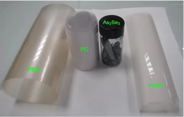
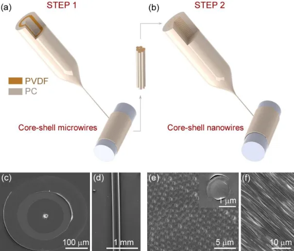
steps if smaller sizes required. Kilometer-long, ordered nanowires which can be fabricated in a broad nanowire diameter range are obtained after the second or higher steps. ... 13 Figure 2.4: Bulk materials that are used in the fabrication of nanostructures. The black color of As2Se3 suggests a very high absorption capacity in visible wavelengths, while polymers generally do not absorb in the visible spectrum. PES and PVDF polymers bear a slight but nonetheless visually distinguishable absorption capacity, in contrast to the highly transparent PC material. ... 15 Figure 2.5: Optical properties of chalcogenide glass, As2Se3, and piezoelectric polymer PVDF. Optical constants of arsenic selenide (As2Se3) and PVDF polymer were measured by spectroscopic ellipsometry. As2Se3 is a high-refractive index material, which enables the confinement of light for Mie resonances in very small dimensions. Thin film interference is also facilitated by As2Se3, regarding the high index difference between the core and the shell. PVDF, on the other hand is a convenient material for core-shell nanostructure applications, because it has a low refractive index and virtually no absorption in visible wavelengths. ... 17 Figure 2.6: Optical properties of polymeric fabrication components, PES and PC, investigated by ellipsometry. PC, which is used as a core polymer in all-polymer core-shell nanowire fabrication, possesses an average refractive index of 1.58, while PES displays a higher average optical index of 1.65. Neither polymer displays significant absorption in the visible spectrum. ... 18 Figure 2.7: Fabrication of glass-polymer core-shell nanowires. Low temperature, multimaterial fiber drawing method is used for the iterative size reduction of a macroscopic layered rod down to core-shell nanowires. Microstructures obtained after the first thermal drawing step are cut in 10 cm strips, arranged in hexagonal arrays of 360 microwires and embedded in dielectric PES prior to a second drawing step. Kilometer-long, ordered As2Se3/PVDF core-shell nanowires are obtained after the second step and can be fabricated in a broad nanowire diameter range (50 nm-1000nm). ... 20
xvi
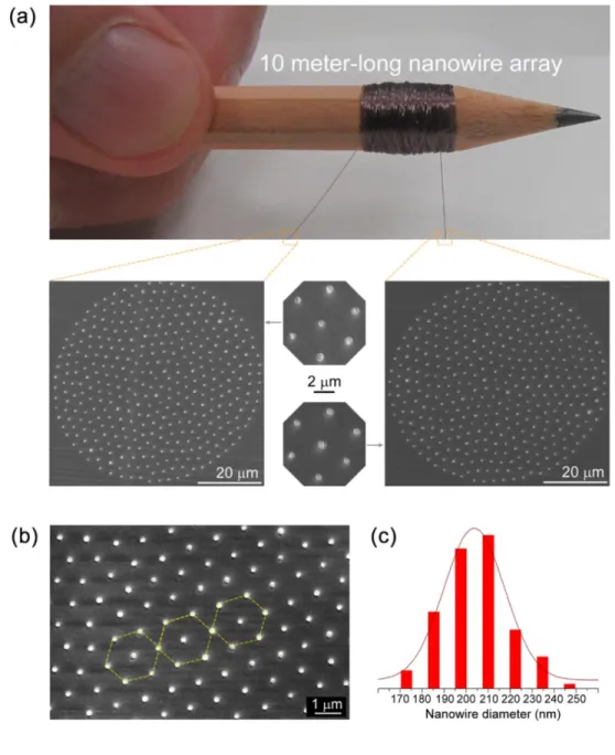
Figure 2.8: Preforms that were used in the fabrication of glass-polymer core-shell nanowires. (a) Step I and (b) step II preforms contain single and 360 fibers respectively. Fabrication of arbitrarily long micro- and nanostructures were accomplished after two iterative steps. ... 21 Figure 2.9: SEM images of step I and step II fibers. Cross-sectional images of (a) step I and (b) step II fibers are obtained by a low temperature, multimaterial fiber drawing method. Free-standing nanostructures obtained by etching the PES sheath by DCM prior to SEM imaging. Longitudinal images of (c) step I and (d) step II micro- and nanostructures are also provided. ... 22 Figure 2.10: (a) A polymer-embedded nanowire array rolled around a pencil truly spans the macroscopic and nanoscale worlds. Cross-sectional SEM micrographs from
both sides of a 10-m-long polymer fiber containing hundreds of As2Se3–PVDF core–
shell nanowires prove that nanowire arrays are axially uniform to less than 1% for macroscopic distances. (b) High-precision hexagonal packing of core–shell nanowires in the polymer matrix. (c) Radial size distribution of the nanowires, shown as a histogram, is uniform with a standard deviation of 6.5%. ... 24 Figure 2.11: Kilometer-long nanowires can be produced with any diameter within the
100 μm-10 nm range while preserving ordered geometry. As2Se3–PVDF core–shell
nanowires scale regularly from 200 μm to 14 nm. ... 25 Figure 2.12: Macroscopic preforms of (a) step I and (b) step II used in the fabrication of all-polymer core-shell nanowires. At the end of second fabrication step, I achieve the production of kilometer long fibers composed of ~500 all-polymer nanowires arranged in a nanostructure array. ... 28 Figure 2.13: Iterative size reduction method used to fabricate all polymer core-shell nanostructures. (a) At the end of first step, core-shell structures with the ~200 µm overall diameters are obtained. (b) A second drawing step is performed using step I microwires to produce core-shell nanostructures displaying a broad size range of 200-2000 nm. Cross-secitonal and longitudinal SEM images of (c,d) step I and (e,f) step II
xvii
fibers display that ISR can be utilized for the production of well-ordered nanowire arrays in macroscale lengths. ... 29 Figure 2.14: Preform preparation of step I fiber is similar to step I of all-polymer core-shell nanowires. However, step II design exhibit significant differences such as, rectangular cross-section design and extraction of outer sheath of step I fibers prior to insertion into step II preform. Around 8 row and 80 column of step I fiber can be inserted into rectangular hole. ... 31 Figure 2.15: Schematics for fabrication of all-polymer photonic crystal structure. First step can be obtained either by rolling polymer films around quartz tube or starting from rod. Second step fabrication slightly different from previous ones. Here rectangular cross-section used in order to increase aspect ratio. Prior to second step fabrication outer layer of step I fibers removed. At the end of step II PVDF embedded PC microwires are fabricated which possess lattice constant of several microns. Using step III by repeating step I and step II procedures lattice constant reduced down to 100-300 nm as required. ... 33 Figure 2.16: Cross-section of step II preform of monolayer structures has very high aspect ratio (30:1) which is utilized in order to maximize number of adjacent nanowires and permit for only single layer of structures to insert. ... 36 Figure 2.17: Schematics for fabrication of all-polymer monolayer structures. First step can be obtained either by rolling polymer films around quartz tube or starting from rod. Second step fabrication relies on insertion of uniform 100 microfibers with 240 micron outer diameter into preform with rectangular cross-section. Prior to second step fabrication holding polymer of step I fibers removed to permit fabrication of PVDF embedded PC microwires. By using step III, diameters of embedded structures are reduced up to 500 nm. ... 37 Figure 2.18: Step II fibers contain globally aligned 360 nanowires inside it. Highly ordered single-layer core-shell nanowire array is obtained after removing outer PES polymer of fiber... 38
xviii
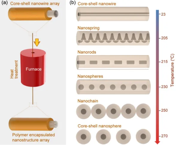
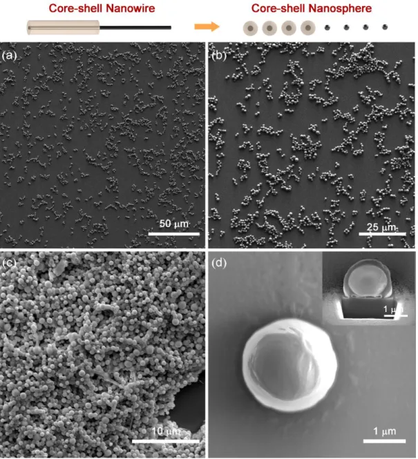
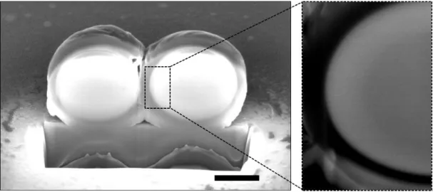
Figure 3.1: Novel nanoschemes produced by structural changes in a nanowire array subjected to heat treatment. Thermal compatibility of chalcogenide glass, PES and PVDF polymers permit the production of different combinations of nanostructures. Gradual increases in temperature result in structural alterations in the nanowire, up to and including the fragmentation of the core region. The structural transition can be halted at any point to obtain the desired nanomaterial configuration. Versatile nanostructures can be obtained by using a suitable combination of temperature, initial nanowire diameter and process duration. The transformation and breakup process is based on the material’s physical parameters, such as viscosity and surface tension. 43 Figure 3.2: Fabrication of core-shell nanosprings can be accomplished by applying heat on a nanowire array. Gradual increases in temperature result in structural alterations in the nanowire, including the deformation of the core region and the consequent production of helical nanostructures. Pitch sizes and periods can be manipulated by altering temperature, initial nanowire diameter and process duration. ... 46 Figure 3.3: Fabrication of shell-embedded nanorods. Further heating of core-shell nanowires (e.g. to 215 °C for t = 2 min and d = 90 nm) results in the fragmentation of the arsenic selenide core into discrete rods inside the PVDF nanoshell. ... 48 Figure 3.4: Fabrication of shell embedded spheres. Temperature above the heat treatment in higher temperatures particularly in 215 °C cause to breaking of core arsenic selenide into periodically separated spheres inside the PVDF nanoshell. ... 50 Figure 3.5: Fabrication of nanochains, accomplished in this case by raising process temperature to 250 °C. Higher temperatures causes the PVDF bridges to separate, resulting in a series of PVDF-arsenic selenide nanospheres within the PES sheath. 52 Figure 3.6: Complete deformation of core-shell nanowires into core-shell nanosphere occurs at temperatures above 270 °C. Core-shell nanospheres are supported by the PES sheath, which is unaffected by applied heat. ... 54
xix
Figure 3.7: Indefinitely long nanostructures. (a) A 2 m nanowire array converted into spherical nanostructures, demonstrating that fiber integrity is not significantly altered by heat treatment, and that nanostructure arrays can be produced in macro-scale lengths by the present method. (b) Cross-sectional and (c) longitudinal images of nanowires (d=450 nm). Produced spherical nanostructures with (d) out of phase, aligned, cross-sectional and (e) longitudinal image. ... 55 Figure 3.8: “Taut” and “slack” fabrication. (a-c) “Taut” fibers produce nanochains with average diameters (500) similar to that of the initial nanowire (450 nm). (d-f) “Slack” fibers, in contrast, produce much higher diameters due to the thermal contraction of the fiber; originated from mass conservation. The SEM micrograph displays nanochains with an average diameter of 400 nm, obtained from 200 nm core-shell nanowires. ... 56 Figure 3.9: Core-only nanoschemes. In addition to (a) core-shell nanoschemes, (b) core-only structures can be obtained by removing the PVDF shell layer. I demonstrate this process by plasma etching an array of core-shell nanosprings, but etchant solvents or drawing core-only fibers may be utilized to the same effect. ... 57 Figure 3.10: Smoothness of microscale structures. Two linked microsphere exhibit smooth surfaces and no apparent irregularities, even under high magnification. Scale bar, 500 nm. ... 58 Figure 3.11: Adjustable instability wavelengths. Different processing times and temperature result in changes in instability wavelengths. Discrete rods displaying varying wavelengths (λ1=140 nm, λ2=240 nm, λ3=580 nm,) were produced following the exposure of a nanowire array to a temperature gradient. Scale bar, 200 nm. ... 59 Figure 4.1: A simulation cell divided into a mesh network. Yee cells are the elemental volumes comprising the mesh structure. ... 62 Figure 4.2: Schematic of the analytical solutions for scattering from a core-shell nanowire. The core medium possesses a higher refractive index than the shell region in my core-shell nanowires. The same equations could be used for nanotubes (or bare
xx
nanowires) by assuming a core (or shell) with the refractive index of air. Subscripts i and s indicate incident and scattered fields, respectively. ... 68 Figure 5.1: Map of resonant Mie scattering in core-shell nanowires. FDTD simulations are performed for (a) TE and (b) TM polarizations. Different resonant modes supported for both polarizations... 77 Figure 5.2: Mie scattering from cylindrical core/shell nanowires. Scattering from a 100 nm core and 25 nm shell structure was analyzed by FDTD simulations to demonstrate the modes supported by the nanostructure geometry. The fundamental mode (TM10) and higher order modes (TM11 and TM21) were present within the calculated geometry ... 78 Figure 5.3: Far-field profile of scattered light for resonant Mie scattering. For TM polarized light, the nanostructure isotropically scatters light. In TE polarization, light is mostly scattered in the back and forward directions. ... 79 Figure 5.4: FDTD-simulated map for resonant Mie scattering and near field profiles of core-shell nanospheres. (a) Scattering map describing the positions of the first three resonant modes. (b) Near field profiles of the first three resonant modes as observed from x, y and z axes. Fields are localized inside the nanostructure and exhibit a leaky-mode behavior. ... 81 Figure 5.5: Map of resonant Mie scattering calculated using real material parameters. Higher orders were observed to disappear, likely due to the higher optical density of arsenic selenide in the smaller wavelengths of the visible region. ... 82 Figure 5.6: (a) Coupled cavity features of a nanosphere array. Waveguides produced by individual spheres exhibit coupled cavity features. (b) Near field profile of scattering modes demonstrate that light can propagate through the spheres by using these modes. ... 83 Figure 5.7: FDTD simulation of fabricated nanoschemes. Scattering profiles of each fabricated scheme is simulated for nanostructure diameters of 200 nm. The use of real
xxi
ellipsometric constants results in the disappearance of higher modes, especially in lower wavelengths where scattering is hindered by absorption by the As2Se3 core. Structure lengths are 3 µm for each scheme. 250 nm rods with inter-structural distances of 200 nm were utilized for discrete rod simulations. While all fabricated nanostructures are expected to yield a red-orange color at 200 nm, pronounced differences are present in their scattering characteristics. ... 85 Figure 5.8: Schematics of experimental set-up for scattering measurements from nanowires and nanospheres. The optical image of a nanowire array is shown. Structures with diameters smaller than 200 nm were obtained using the dark field mode of an inverted microscope. The scattering spectrum was taken by a UV-Vis spectrometer coupled to the microscope. ... 86 Figure 5.9: (a) A novel thermal size reduction technique is used to obtain indefinitely long, scalable core-shell nanowires. The structure consists of a high-dielectric semiconducting (As2Se3) core, a piezoelectric polymer (PVDF) shell and a high-temperature thermoplastic (PES) cladding. The structures show native structural coloration based on their size-dependent properties. (b) Core-shell structures, when scaled down to a diameter range between 30-200 nm, show resonant small particle scattering. Mass-produced, indefinitely long and large-area core-shell nanowire arrays can be colored by (c) Mie scattering . ... 88 Figure 5.10: (a) TEM images of polymer embedded As2Se3/PVDF core-shell nanowires. (b) Size-dependent Mie scattering from 35 nm (blue), 42 nm (green), and 175 nm (red) core-shell nanowires. (c) Spectroscopic dark field scattering measurements from these three core-shell nanowires show size-dependent resonant peaks at 470 (blue), 530 (green), and 700 (red). (d) Numerical FDTD calculations of scattering from these nanowires agree well with the measurements. Inset: Resonant modes are identified using FDTD simulations. In the calculations, I used wavelength-dependent refractive indices and extinction coefficients obtained from spectroscopic ellipsometry measurements. ... 89
xxii
Figure 5.11: Large-area core-shell nanosphere arrays engineered for blue, green and red hues, with average diameters of ~130, 170 and 220 nm, respectively. (d) Scattering from colored nanostructures measured by inverted dark-field microscopy. (e) FDTD simulation technique used for the verification of experimental results. (f) Analytical solutions for light scattering from spherical core-shell nanostructures modeled with Lorenz-Mie theory. Analytical and simulation results overlap, and are consistent with measurement data. Collective scattering from large area spheres with narrow size distributions result in uniform coloration and small shifts in scattering spectra. Ellipsometric material parameters were used in FDTD and analytical calculations. 91 Figure 5.12: Large-area in-polymer coloration of globally oriented nanostructures. Resonant Mie scattering-based coloration is observed on various fabricated nanoschemes. High uniformity and smoothness is paramount for large-area coloration, and result in size dependent color shifts when compromised. Present fabrication method is able to eliminate such structural errors (a-f). Sizes are ~200 nm for all cases. ... 93 Figure 6.1: Mie scattering from nanostructures. (a) Schematic illustration of light scattering from core-shell nanostructures. Near-field profiles for scattered fields of (b) resonant and (c) non-resonant regimes. In the resonant regime, light confines within nanowire and is then scattered in a leaky mode. However, for low-refractive indices, light cannot be trapped inside nanowires and is instead scattered in the forward direction. (d-e) The transition from resonant to non-resonant Mie scattering regimes can be observed by reducing the refractive index of the nanostructure. While changes between the modes of TE and TM polarizations is observed in higher refractive indices, scattering maps are nearly identical for the low refractive index medium for both polarization types. ... 96 Figure 6.2: NRM scattering maps of core-shell polymer nanowires for (a) TE and (b) TM polarizations. Extending the wavelength and diameter ranges for a fixed n of 1.5 in Figure 6.1d,e results in the appearance of lower orders. Electric field profiles of corresponding orders of (c) TE and (d) TM polarizations exhibit strong directional
xxiii
scattering. Field profiles confirm the non-resonant nature of the NRM scattering regime. ... 97 Figure 6.3: NRM scattering in various geometries. (a) NRM scattering in bare nanowires. Electric field profiles of first order of TE and TM polarizations exhibit forward scattering behaviour, as would be expected. (b) Nanotube geometry is another interesting structure for the observation of this scattering regime. Field profiles of NRM scattering from this geometry differ slightly from the nanowire case, although they also exhibit forward scattering behavior. Nanotubes are one of the most favorable geometries in microfluidics, and NRM scattering is therefore promising in this field. Inner/outer diameter ratio of the nanotube is 1:1.5 for all calculations. (c) For sphere geometry, non-resonant field distribution verifies forward-scattering feature as in 1D nanostructure cases... 99 Figure 6.4: Comparison of analytical solutions with FDTD simulations. Analytically solved scattering equations for both (a) TE and (b) TM polarizations were compared with FDTD simulation results. The method used for analytical solutions is based on vector wave harmonic expansion of scattered light. Simulated results are in good agreement with theoretical calculations. Nanowires used for comparison have core diameters of 340, 400, 520 nm for blue, green, and red coloration, respectively. ... 100 Figure 6.5: Optical properties of NRM scattering. (a) Coupling-free scattering can be obtained for illumination perpendicular to the coupling axis (as shown in the inset). (b) Mode splitting is observed when light is incident on coupled nanowires. (c) Scattering from low refractive index nanostructures displays a polarization independent behavior. (d) Far-field intensity profiles indicate that light mostly scattered along the forward direction. Very high forward to backward scattering ratios are obtained for both polarizations. ... 102 Figure 6.6: Coupling-free scattering. Side-by-side nanowires do not induce optical coupling, which is markedly different from resonant Mie scattering. For both (a) TE and (b) TM polarizations scattering spectrum is unaffected from number of side-by-side core-shell nanowires. Same results hold for bare nanowires (c,d). ... 103
xxiv
Figure 6.7: Field profiles of coupled nanowires. (a) Near field profile of scattering from a single core-shell nanowire. (b) The field profile corresponds to a 550 nm peak in Figure 6.5a. Electric field distribution within the core-shell structure is almost unaffected from the number of nanowires that are arrayed side-by-side. (c-d) Scattered light exhibits coupled cavity behavior in overlapping nanowires. Profiles in (c) and (d) correspond to 1060 nm and 450 nm peaks in splitting, respectively shown in Figure 6.5b. ... 104 Figure 6.8: Measurement setup for structural coloration. Schematics of experimental set-up used for scattering measurements of polymer nanowires. Optical microscope images of individual colored nanowires are obtained in the bright field mode of an inverted microscope. The scattered light is collected by a UV-Vis-NIR MAYA spectrometer coupled to the microscope. ... 105 Figure 6.9: Structural coloration of polymeric nanostructures. Light scattering from core-shell nanostructures designed for red, green and blue coloration was investigated experimentally and theoretically. (a) Optical microscope images of colored nanostructures. Red, green and blue hues were observed on nanowires with core diameters of 340, 400, and 520 nm, respectively. (b) Scattering measurements performed by using inverted optical microscope in bright field mode (Detailed measurement setup is given in Figure 6.8). (c) Scattering from low refractive index nanostructures are simulated by using a FDTD technique with ellipsometric constants. (d) An analytical solution based on the vector wave harmonic expansion of scattered light is developed for core-shell geometry. Experimental measurements agree well with the analytical and simulated results. ... 106 Figure 6.10: Nano-blade lithography uses the focusing feature of NRM scattering in order to expose the photoresist in sub-wavelength sizes. Consequently, 1D grating structures or holes can be fabricated. ... 108 Figure 7.1: Nanoshell interference mechanism is demonstrated in spectroscopic FDTD simulations of size-scalable As2Se3/PVDF core-shell nanowires, using TM polarized light. Nanoshell interference is effective for shell size in the 150-300 nm range. The
xxv
formation of reflection peaks is due to shell layer interference. Secondary high frequency interference in larger nanowires does not compromise coloration. ... 111 Figure 7.2: Theoretical analysis of structures associated with cylindrical core-shell nanowires. Reflection spectra of three different geometries were determined by FDTD simulations. Reflection from the As2Se3 substrate (red) is constant throughout the spectrum, as expected from Fresnel equations. Spectra of thin film interference for PVDF film on As2Se3 substrate (blue), and shell on nanowire (green) exhibit similar behaviors and peak in closest spectal points. Shell and core thicknesses are set at 250 nm and 1000 nm, respectively. ... 112 Figure 7.3: Nanoshell interference phenomenon in coated microspheres. Multiple reflections from different material interfaces result with constructive and destructive interferences. First two order of interference appear in the calculated size and wavelength range. Rapid and slow oscillations are originated from core and shell region respectively. During calculations, sphere diameter is taken constant as 1 μm. ... 114 Figure 7.4: (a) A novel thermal size reduction technique is used to obtain indefinitely long, scalable core-shell nanowires. The structure consists of a high-dielectric semiconducting As2Se3 core, a piezoelectric polymer (PVDF) shell and a high-temperature thermoplastic (PES) cladding. The structures show native structural coloration based on size-dependent properties. (b) Structural coloration based on non-resonant interference for shell sizes between 150 and 300 nm, where coloration results from multiple reflections from core-shell interfaces. ... 116 Figure 7.5: Schematics of the experimental set-up for reflection measurements. Optical image and reflection data were obtained using the bright field mode of an optical microscope. The reflection spectrum was taken by a UV-Vis spectrometer coupled to the microscope. ... 117 Figure 7.6: (a) SEM image of the polymer embedded As2Se3 (core)/PVDF (shell) microwire/nanoshell. (b) Size-dependent coloration from the shell layers of the 170
xxvi
nm (blue), 195 nm (green) and 270 nm (nanoshells). (c) Spectroscopic bright field reflection measurements from the three core-shell structures show size dependent interference peaks at 470 (blue), 520 (green) and 750 (red). Modulation in the red spectra is due to secondary interference from the core region. (d) FDTD simulations are in agreement with the measurements. ... 118 Figure 7.7: Core-shell microspheres colored via the nanoshell interference. Nonuniform shell thicknesses cause reflection of different colors. Vivid hues of any color can be obtained via the altering the thickness of shell region. Microsphere chain observed to colored via the same effect (righ image on the top). Colored spheres possess core diameter of 1-2 μm. ... 119 Figure 7.8: Shell size determination, an interesting application of nanoshell interference. As each color corresponds to specific shell thickness we can use this feature in order to determine thicknessess of shell layer without using any complex characterization technique. ... 121 Figure 7.9: Depending on core material light can be reflected from interfaces in distinct amounts which can be used for discriminating core material composition. Three representative refractive indices 4.5, 3.5 and 2.5 which corresponds to a-Si, As2Se3 and As2S3 glasses can be easily detected according to their brighntess.. ... 122 Figure 8.1: Optical microscopy images of mallard neck feathers. As magnification, increases the color of the mallard feather changes from green to blue, which suggests that iridescence is responsible for the observed color. Macroscopic coloration is induced by nanoscale features exist in the barbules... 125 Figure 8.2: Cross-sectional and longitudinal SEM images of mallard feather barbule. Hexagonal arrays of rods are observed to be distributed throughout the outer side of barbule. Melanin rods are discrete within the barbule and their lengths are in submicron range. ... 126 Figure 8.3: (a) Scheme representing the distribution of melanin rods embedded in the keratin matrix. Lattice constant (λ) and diameter (d) are main parameters in the
xxvii
photonic crystals. (b) SEM image of hexagonal arrays of rods in mallard feather. Lattice constant and diameter oberved from SEM images are around 210 nm and 170 nm respectively. ... 127 Figure 8.4: (a) Simulation of reflection by neck feather barbules. Lattice and rod diameter values were measured from SEM images. (b) It is clear that a partial band-gap exists in the green portion of the spectrum. This is the cause of the green color observed in mallard feathers. ... 129 Figure 8.5: Experimental and simulation results of mallard feather. It is apparent that my observations and simulation results are in good agreement. FDTD simulation is performed for material parameters obtained from SEM images of mallard drake feather. ... 130 Figure 8.6: SEM images of fabricated nanostructures. As a result of three iterative drawing steps lattice constants of photonic crystals reached into nanoscale. In particular SEM image represent photonic crystal that possess lattice constant of ~200 nm. ... 133 Figure 8.7: Functional biomimicry of mallard neck feathers. (a) SEM images reveal the hexagonal distribution of PC rods inside the PVDF matrix. (b) Distinctive colors observed under light microcopy confirm the presence of photonic crystal effects for lattice constants around 200 nm. (c) Reflection measurementsof colored photonic crystal structures. (d) FDTD simulations performed for a lattice constant of 210 nm and diameter 170 nm. ... 134 Figure 8.8: Iridescence in mimicked photonic crystal fiber. As I increase magnification of light microscope which corresponds to increasing of angle of incident light, green colors transform into blue color as result of present phenomenon. ... 135 Figure 8.9: (a) Fiber containing several hundreds of PC rods located inside a circular zone. (b) It is demonstrated that the photonic crystal effect can be observed even with a circular structure design. ... 135
xxviii
Figure 8.10: (a) Photonic crystals fabricated from microwires produced by nucleated ISR. (b) These structures are also well-suited for photonic crystal-based coloration. ... 136 Figure 9.1: Absorption enhancement by all-polymer core-shell nanowires. Core-shell nanowire arrays were simulated on top of a conventional solar cell composed of a silver back contact, an AZO layer, an amorphous silicon absorbent and an ITO front contact. Textured surface and NRM based coupling effects (dominant on the left and right side of plot, respectively) result in enhanced absorption. TE polarization is used for the investigation of absorption enhancement, TM polarization yields similar results. ... 140 Figure 9.2: Nanostructure geometry has profound implications on the amount of absorption enhancement. Bare and core-shell nanowire geometries exhibit significant differences in enhancement rates. Absorption enhancement values of 16.5 and 18.5% are observed for bare and core-shell nanowires, respectively... 144 Figure 9.3: Effect of core-shell nanowire sizes on absorption enhancement, investigated using three nanowire diameters. Enhancement values are observed to be around 15%, 17.5 % and 14% for 500, 600 and 700 nm structures, respectively. .. 145 Figure 9.4: Nanostructure-mediated absorption enhancement of As2Se3. The enhancement rate is calculated to be ~24%. Both NRM scattering and textured surface effect participate in the absorption enhancement. ... 147 Figure 9.5: (a) Schematic used in the experiment. (b) Absorption measurement for As2Se3 thin film with and without core-shell naowires. Observed enhancement is around ~6 %. (c) Optical microscope images of coated silver, thin-film As2Se3 and monolayer nanowire layers. ... 148 Figure 9.6: As we increase thickness of As2Se3 thin film its aborption profile red-shifts. All-polymer core-shell nanowires with diameters of 600 nm induce absorption enhancement of ~13.5 %. Obviously, textured effect is responsible in this enhancement and NRM scattering cannot contribute into this due to thicker absorbent layer. ... 149
xxix
Figure 9.7: Contact angle measurement of (a) PVDF film and (b) nanowire array. PVDF polymer is hydrophobic by itself due to containing fluoride. However, core-shell nanowires add two degree of roughness which are originated due to; submicron roughness of core-shell nanowires and nano-roughness of PVDF shell. ... 150 Figure 9.8: Sensitivity parameters of NRM scattering. (a) Rapid shifts in scattering spectra can be observed by changing the refractive index of the medium surrounding core-shell structures with core radii of 300 nm, and correspond to high sensitivity values. (b) Size-dependent sensitivity values (left and bottom axes) plotted with medium-dependent shifts of the center wavelength (right and top axes)... 152 Figure 9.9: Changes in nanoshell interference-based reflection values depend on the refractive index of the surrounding medium, which may be utilized in optical sensors. Reflection intensity determines the performance of sensitivity. ... 154 Figure 10.1: Material dispersion is derived from material parameters of As2Se3 glass (n,k) by implementing Sellmeir model. Dispersion in the 1.55 μm wavelength is very high and can distort femtosecond pulse in short propagation distances. ... 160 Figure 10.2: Dispersion engineering with waveguide dispersion and material dispersion. Zero dispersion point for 1.55 μm wavelength calculated to be at ~1 μm core diameter. ... 161 Figure 10.3: Zero dispersion points for different operating wavelengths. Material dispersion alters as the wavelength changes. Therefore waveguide size required to be set accordingly in order to compensate material dispersion with waveguide dispersion. ... 161 Figure 10.4: Supercontinuum generation from nanowire array. Nanowire array induce efficent supercontinuum generation and supply higher power output in compare to single nanowire under same illumination conditions. Pulse width of source defined as 250 fs. Supercontinuum generation phenomenon is associated with self-phase modulation effect. Third and higher harmonics generation appear in the left portion of spectrum. ... 163
xxx
List of Tables
Table 4.1. Generating functions of all three regions within the core-shell nanowire. 70 Table 8.1. Material selection for structural coloration. All-polymer structures are suitable for mimicking process due to low refractive index contrast. ... 131 Table 9.1. Different designs for light trapping. All-polymer core-shell nanowires induce absorption enhancements of ~14% for a-Si and ~20% for c-Si. Enhancement value are almost independent of polarization type. ... 142
1
Chapter 1
Introduction
Light-matter interactions are an integral part of our life. They play a crucial role in many biological systems (such as photosynthesis, vitamin D synthesis and circadian rhytms), are responsible for mediating many natural phenomena (such as rainbow, glory and airglow) and form the basis of processes such as lasing, diffraction, interference, absorption, refraction and reflection, which are harnessed for human convenience in such devices as eyeglasses, phones, sensors and LEDs. While light-matter interactions in the macroscale are well-characterized, developments in nanotechnology have spurred the discovery of a vast number of new light-matter interactions that can only be observed under smaller scales (while electromagnetic effects are scalable across a wide size range, nanoscale structures must be utilized for these effects to occur in the visible region of light). In addition, nanostructures may also display a variety of unique effects by virtue of their size alone, as quantum effects become significant at the size scales involved. As such, nanoscale materials have received much attention in the recent decade for the
2
reproduction of a variety of optical phenomena in the visible range, for both academic research and practical applications.
In optics, the minimum size at which a structure is capable of effecting the concentration of light is known as the diffraction limit [1]. In other words, light can only propagate through structures above a certain size limit, which is equal to half of the propagating wavelength. However, metal nanostructures are capable of breaking this size limit by the confining the photons into deep-subwavelength structures [2] via the cluster oscillation of free electrons. The investigation of this phenomenon is the study area of plasmonics and constitutes an important part of nanophotonics. Dielectric materials are generally considered preferable to metals in optical applications due to their higher biocompatibility, low optical losses, broad material options, cost-effectiveness and flexibility. While the diffraction-limit problem renders it difficult to utilize nanostructures with dielectric compositions for optical purposes, absorption by and scattering from small particles which result with leaky-mode resonances can bypass such issues. Such interactions fall in the domain of the Lorenz-Mie theory [3]. In addition, the diffraction limit can also be bypassed by using dielectric materials in nanostructure arrays, which behave as an effective medium [4] and can be characterized by effective medium models, or fabricating them as periodic structures to display the photonic crystal effect [5]. Likewise, light can be guided inside a high refractive index dielectric structure at selective wavelengths, which is different from the fiber guiding mechanism [6]. The multiple scattering phenomenon, an effect similar to but distinct from photonic crystals and individual particle scattering, [7] can also be utilized for the optical functionalization of dielectrics.
Advances in nanofabrication techniques have resulted in the discovery of a vast variety of novel optical effects, each associated with a unique set of application areas. Nanomaterials displaying such unique optical phenomena can be utilized in the development of novel designs and devices for such diverse purposes as the engineering of nanoscale structures for the enhancement of light absorption
3
efficiency or the fabrication of large-scale nanostructure arrays exhibiting structural coloration. Among nanoscale materials, nanowires and nanospheres are arguably the most studied configurations and comprise outstanding media for the investigation of light-matter interactions, having been utilized in numerous occassions for the practical utilization of nanoscale optical phenomena [8,9].
Nature also plays a key role in the progress of optical nanoscience. Photonic structures in biological systems are generally in the nanoscale, and may display a diverse array of optical features. Photonic crystals observed in peacock feathers [10] and the anti-reflective surfaces [11] displayed by the eyes of nocturnal insects are two well-known examples of nanoscale optical phenomena in biological systems. These structures can be mimicked by using advanced fabrication techniques [12].
Consequently, advances in nano-optics rely on both the investigation of biological structures and conventional materials engineering strategies. This combination is expected to play a key role in the solution of many global problems, and can be alleviate pressing energy, food, environment, communication and health issues experienced by the modern world.
Numerous fabrication techniques exist for the production of nanostructures with zero-dimensional (0D), one-dimensional (1D) and/or two-dimensional (2D) features. Thin film nanostructures [13] can be fabricated via physical techniques, such as laser ablation and electron beam evaporation, or chemical techniques, such as chemical vapor deposition and sol-gel processing methods. Many top-down [14,15,16] and bottom-up [17,18,19] techniques are also known for the fabrication of 0D and 1D nanostructures. Top-down fabrication methods for such purposes include lithographic, AAO template and electrospinning methods, while many chemical techniques constitute examples of bottom-up approaches for nanostructure fabrication. Existing methods, however, are constrained by several limitations, which include:
4
Alignment: Nanostructures produced by current fabrication methods are generally
randomly oriented and require post-synthesis processing. A number of techniques [20,21] have been developed to overcome this problem. However, these specialized methods are often expensive and cannot be applied for large-scale production of aligned nanomaterials.
Material constraints: Fabrication techniques are often inapplicable to all but a
select number of materials [22,23], and fabrication steps frequently require all material components involved to display a specific physical property to function. Such material properties include elasticity (electrospinning), selectivitiy (lithography), chemical compatibility and/or high-temperature stability (chemical techniques).
Length and mass production: Many nanofabrication methods can produce
nanostructures in lengths of up to several millimeters [24]. However, the mass production of 1D nanostructures remains a challenge and current fabrication methods are generally incapable of scaling up their production output.
Uniformity and smoothness: Nanofabrication techniques frequently produce
structures with rough or non-uniform surfaces problem [25,26]. This is especially undesirable in light-matter interactions, where surface irregularities may cause unwanted spectral shifts or optical aberrations.
Fabrication speed and cost: Nanoscale structures are must be fabricated rapidly
and without incurring extravagant costs in order to fully integrate themselves in our daily lives. However, some fabrication methods may require longer processing times, and many others are only useful for the production of prototypes [27,28,29] due to their prohibitively expensive costs.
Nanostructure diversity: As each nanostructure arrangement is associated with a
number of unique phenonena, the production of novel nanostructure configurations is one of the driving factors in nanotechnology [30]. Many novel electrical, optical, mechanical and thermal properties can only be observed in nanoscale materials
5
displaying specific shapes and arrangements. However, many nanofabrication techniques are applicable for only a select number of nanostructures, and cannot be utilized for the production of complex nanostructure configurations.
In this thesis, I focus on the investigation of new fabrication techniques capable of fulfilling the rigid requirements expected of nanomaterials suitable for utilization in emerging optical applications. To this end, we developed a cost-effective, rapid and high-throughput top-to-down approach, which we call Iterative Size Reduction (ISR), capable of producing arbitrarily long, uniform, globally aligned nanostructures [31]. I demonstrate this method to be successful in the fabrication of hard-to-produce glass/polymer and all-polymer core-shell nanowires. I also show that all-polymer photonic crystal structure and monolayer nanowires can be produced by modifying this approach.
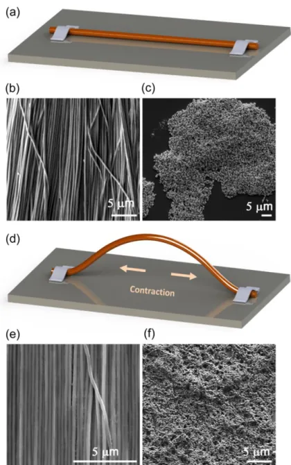
Then I demonstrate a combined iterative size reduction-thermal manipulation method by which a large diversity of indefinitely long, globally parallel, complex nanostructure arrays with high surface uniformity and low optical variation can be fabricated from PES-embedded core-shell As2Se3-PVDF nanowires [32]. Nanosprings, nanoshell-embedded discrete nanorods and nanospheres, and nanochains are produced in succession by a hitherto-undescribed, Plateau-Rayleigh instability-mediated deformation, eventually culminating in the fragmentation of the nanostructure array and the formation of core-shell nanospheres. Structure sizes, profiles, instability wavelengths and optical properties can be modified by minor alterations in process temperature and duration. As such, a great diversity of nano-configurations with highly desirable features (i.e., smoothness, length, uniformity, and alignment) can be obtained by using this combined thermal nanofabrication technique.
I observe and report a variety of optical phenomena that take place in fabricated novel core-shell nanostructures, which I engineer for several important applications. Resonant Mie scattering is a well-known optical phenomenon and results from the
6
interaction of light with small, high–refractive index particles, and I produce and characterize a diverse set of core-shell nanoschemes for structural coloring based on this phenomenon [33]. I also observe that low-refractive index materials in a specific size range are capable of displaying a non-resonant form of Mie scattering [34], report for the first time that thin film interference occurs on the core-shell interface of micron-scale glass-polymer spheres [33], utilize all-polymer core-shell nanowires to mimic the unusual photonic crystal structures observed in the head feathers of
Anas platyrhynchos drakes [35], demonstrate the sensing capabilities associated with
NRM scattering and the nanoshell interference phenomenon, show that all-polymer core-shell nanowire coatings are capable of enhancing light absorption in solar cells via NRM scattering and the textured effect [36], and combine the inherent nonlinearity of chalcogenide glasses with our ability to produce nonlinear arrays of nanowires to generate broad-spectrum supercontinua with high power throughputs [37].
This thesis is organized as follows: In Chapter 2, I describe the details of a novel fabrication technique, Iterative Size Reduction (ISR), for the synthesis of 1D core-shell nanostructures, and detail the materials utilized throughout the fabrication process. The fabrication mechanisms of glass-polymer and all-polymer core-shell nanowires, photonic crystal and monolayer structures are elaborated in this chapter. In Chapter 3, I demonstrate that ISR-produced glass-polymer nanowires are modified into a diverse array of core-shell nanostructures via Plateau-Rayleigh instability-mediated deformation following heat treatment, and characterize the temperature region in which these nanoparticles are produced from core-shell nanowires. In Chapter 4, I detail the analytical and numerical techniques that I utilized in order to predict the behavior of light in fabricated core-shell nanostructures. In addition, this chapter features detailed analytical solutions for the characterization of scattering from core-shell nanostructures. In Chapter 5, I explain the theoretical background of the Resonant Mie scattering phenomenon and how it can be engineered for
7
observation of structural coloration in the diverse core-shell nanoschemes. In Chapter 6, I characterize a novel, non-resonant form of Mie scattering in low-refractive index materials and discuss the potential of this phenomenon in photonics applications. In Chapter 7, I prove that an analogue of the thin-film interference phenomenon, which is called nanoshell interference, occurs on the core-shell interface of glass-polymer spheres. In Chapter 8, I investigate and imitate the unusual photonic crystal structures observed in Anas platyrhynchos neck feathers. In Chapter 9, I provide the theoretical and experimental demonstration of light absorption enhancement by all-polymer core-shell nanowires, and discuss sensor applications of NRM scattering and nanoshell interference phenomena. In Chapter 10, I present a proof-of-concept scheme for the generation of supercontinua using nanowires of highly nonlinear chalcogenide glasses, and utilize dispersion engineering procedures to design a nanowire array displaying high-performance spectral broadening. In Chapter 11, I summarize the topics investigated throughout the course of this thesis.
8
Chapter 2
Iterative Size Reduction Technique for
Production of Nanostructures
2.1 Iterative Size Reduction Technique
The method described in this chapter, Iterative Size Reduction (ISR), is a recently developed top-down nanofabrication technique [31] involving the repeated reduction of macroscopic structure sizes by a series of successive drawing steps. This technique is inspired by the Taylor wire drawing process [38], which we successfully improve and utilize as a nanotechnology toolkit for the production of 1D nanostructures. Due to the physical properties of used materials, fabrication of nanostructures can be performed at relatively low temperatures (approx. 300 °C maximum). Nanostructures are formed entirely by physical interactions, mediated primarily by viscosity and surface tension.
9
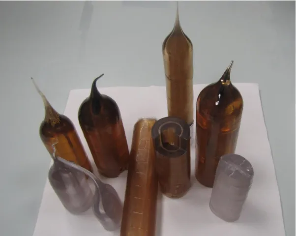
Figure 2.1: Photographs of macroscopic preforms. Preforms are macro prototype of fabricated micro- or nanostructures. The design of preform may change depending on the purpose of fabrication and geometry of nanostructures.
As such, this method does not rely on the chemical properties of material components, and can be utilized for a wide range of materials.
The nanostructure produced by this approach are closely match the initial macroscopic preform in profile thanks to mutually compatible viscoelastic properties of the material set used, which also prevents the structures from collapsing and results in the creation of uniform nanostructures.
10
Amorphous materials are advantageous for thermal nanofabrication method, including ISR, due to their continuous glass transition temperatures. As such, the present top-down methodology can be utilized to draw chalcogenide based glasses with a variety of polymeric materials.
The ISR procedure involves a macroscopic preform, prepared prior to fabrication, being reduced to smaller scales using a novel fabrication system designed for thermal drawing. The fabrication process may utilize several iterative steps in order to obtain the required sizes. At the end of each step, structures are characterized by electron microscopy prior to their use in subsequent steps.
Preforms (Figure 2.1) are macroscopic structures that form nanostructures following multiple elongation and size reduction steps. They are composed of two or more functional layers. Conventional preforms consist of a glassy material filling contained by an outer polymer shell. Here, the glass serves as a functional component and can be selected according to the electrical, optical, mechanical and/or thermal properties required of the micro- or nanoscale material. The outer polymer sheath provides flexibility and makes the handling of fabricated structures feasible. These preforms also can be produced by (a) wrapping the core and shell layers around a glass rod, which is subsequently removed prior to fabrication (“tube” synthesis), or (b) wrapping two polymer layers (the sheath and shell regions) and a glass or polymer-based filling material (the core region) successively around each other (“core-shell” synthesis). Depending on the purpose of fabrication, the sheath region can be removed by etchant treatment and free-standing bare nanowires, core-shell nanowires and nanotubes can be obtained. In-fiber cases nanostructures produced by this method are also very useful in number of applications. Further alterations in starting configuration (i.e. multilayered structures or structures with square, triangular cross-sections) can also be utilized for nanostructure synthesis. Following their production, macroscopic structures are held in the furnace for the consolidation process to occur. Consolidation is performed under vacuum to conserve structural
11
Figure 2.2: Home-built fiber tower system designed in order to reduce sizes of macroscopic preforms. The 2.5 m tower consists of thermally isolated double zone furnace, feeding, capstan, thickness, and tension meter units. Furnace temperatures may exceeds 300 °C which is sufficient for the fabrication process due to the low glass transition temperatures of the materials utilized. A mass is hanged from the top of the perforated preform in order to apply mechanical stress and facilitate the drawing of preform when a certain material viscosity is reached. For uniform heat treatment, the position of preform is arranged by using the x-y stage. Down-feed and capstan speeds are arranged prior to fiber drawing. Sizes of inner structures are controlled by altering the outer diameter of the fiber. Tension is used as a feedback for the settings of down-feed, capstan and furnace units. Polymer fiber thickness is measured with a laser micrometer, and fiber tension by a transverse tensiometer.
12
homogeneity and prevent defect formation, and sufficient time is provided for the polymer layers to fuse into a distinctive sheath region.
Consolidated preforms measuring several centimeters in diameter are then thermally drawn in a custom-built fiber tower system. The fiber tower consist of several important structural components, which are detailed in Figure 2.2. Preform positions are fixed with a holder and, if necessary, can be changed by a x-y stage for uniform heat treatment. Preforms are generally inserted 8 cm into the top of the furnace prior to heat treatment. This distance corresponds to the position of the hot zone of our furnace, which has an effective length of 2.5 cm. Amorphous preforms are conventionally drawn in a material-specific temperature region in which viscous forces are balanced with an applied mechanical stress. This stress originated from a load hanged to the bottom of the preform. When the mechanical stress (weight of mass) exceeds the viscous forces present (which decrease due to applied heat) the perforated portion of the preform stretches slightly and is cut off. The tapered section of the preform is wrapped around reels as described in Figure 2.2. Following the fixation of the tapered section, the capstan rotated in clockwise direction and a down-feed speed value is supplied. Here temperature, down-down-feed and capstan speed are engineered to obtain the structure sizes required without deforming the initial structure profile or breaking the fiber. Structure sizes are controlled by monitoring total fiber diameter using a laser micrometer. The tension on the fiber continuously measured in order to prevent fiber rupture.
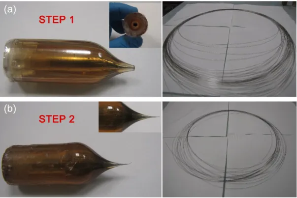
Microstructures obtained after step I cut and prepared for the second step of fabrication (Figure 2.3). Composite fibers with outer diameters of several hundred microns are embedded in a polymer sheath (a hollow preform prepared in order to hold first step microfibers) in hexagonal arrays of several hundred microfibers and redrawn to produce indefinitely long nanowire arrays. The process can be repeated for subsequent steps if smaller sizes are required. Reduction factors between 25 to 500 can be obtained in each drawing step.
13
Figure 2.3: Low temperature, multimaterial fiber drawing method used for the iterative size reduction of a macroscopic layered rod down to nanoscale. Microstructures obtained after the first thermal drawing step are cut in cm-scale strips, arranged in hexagonal arrays of several hundred microwires and embedded in dielectric polymer sheath prior to a second drawing step. Same procedure repeated for third or higher steps if smaller sizes required. Kilometer-long, ordered nanowires which can be fabricated in a broad nanowire diameter range are obtained after the second or higher steps.
14
Very high reduction factors, however, render the handling and subsequent drawing process difficult, and very small reduction factors hinder efficient fabrication efforts. Ordered and globally aligned in–fiber nanostructures can be obtained at the end of designed multi-step fabrication process. These fibers display ideal characteristics for their direct use in a diverse array of applications without using post-synthesis assembly techniques that drive up fabrication costs.
This step-by-step drawing technique allows the production of indefinitely long nanostructures with aspect ratios as high as 1012. This fabrication method also allows the large-scale production of these nanostructures, which are well-suited for flexible surface applications due to their outer polymer layer. ISR-fabricated nanostructures are highly uniform and possess smooth surfaces due to the thermal origin of fabrication. In addition, this technique is very cheap and rapid compared to other nanofabrication techniques.
2.2 Chalcogenide Glasses and Polymeric Materials
Materials I use in the production of nanostructures are amorphous and suitable for described thermal drawing process due to their thermoplastic properties. Chalcogenide glasses have low softening points and continuous glass transition temperatures, which render it possible to co-draw these materials with high-temperature engineering polymeric materials.
Chalcogenide glasses can be synthesized from individual elemental components using high-temperature furnaces. I prefer to use arsenic selenide (As2Se3) glass, in the fabrication of glass-polymer core-shell nanowires. To this end, As2Se3 rods, 4 mm in diameter and 8 cm in length, are prepared by melting commercially bought glasses (Amorphous Materials) in a vacuum-sealed quartz tube followed by water quenching.