Automated parallel high-speed atomic force microscopy
S. C. Minne, G. Yaralioglu,a)S. R. Manalis, J. D. Adams, J. Zesch,b)A. Atalar,a) and C. F. Quatec)
E. L. Ginzton Laboratory, Stanford University, Stanford, California 94305
~Received 27 January 1998; accepted for publication 2 March 1998!
An expandable system has been developed to operate multiple probes for the atomic force microscope in parallel at high speeds. The combined improvements from parallelism and enhanced tip speed in this system represent an increase in throughput by over two orders of magnitude. A modular cantilever design has been replicated to produce an array of 50 cantilevers with a 200mm pitch. This design contains a dedicated integrated sensor and integrated actuator where the cells can be repeated indefinitely. Electrical shielding within the array virtually eliminates coupling between the actuators and sensors. The reduced coupling simplifies the control electronics, facilitating the design of a computer system to automate the parallel high-speed arrays. This automated system has been applied to four cantilevers within the array of 50 cantilevers, with a 20 kHz bandwidth and a noise level of less than 50 Å. For typical samples, this bandwidth allows us to scan the probes at 4 mm/s. © 1998 American Institute of Physics.@S0003-6951~98!01618-0#
As the semiconductor industry continues to shrink its design rules, new advanced metrology and lithography tools become increasingly important. There has been much recent work on applying the well-known techniques of scanning probe microscopy ~SPM! to these problems. The crux of these efforts is to maintain the resolution and precision of the probe-based system while increasing its capacity, in terms of area scanned in a given time, to a level that is viable for commercial purposes. The throughput of the scanning probe microscope system has been enhanced by moving to parallel operation with arrays, and by increasing the scanning speed of each probe.
The parallel system is a direct approach to increasing the speed of the SPM system since the throughput of a micro-scope is increased in direct proportion to the number of tips in an array. Integrating deflection, or force, sensors onto the cantilever simplifies the operation of the parallel system be-cause it reduces the necessary alignment and maintenance required for operation. The piezoresistive atomic force mi-croscope~AFM! sensor, developed by Tortonese1et al., has been incorporated into parallel arrays and has been used for imaging and lithography.2 Many other groups have adopted the piezoresistive sensor for probe systems. Lutwyche3et al. has fabricated and used two-dimensional arrays of piezore-sistive cantilevers. Parallel piezorepiezore-sistive cantilevers for data storage applications have been fabricated by Chui4et al. and Ried5 et al. Parallel optical lever cantilever sensors have been demonstrated by Lang6 et al. for use in imaging and other sensing applications.
In most probe systems, throughput is limited by the speed at which the tip can be scanned over the sample sur-face. For constant force imaging this speed is generally lim-ited by the speed of the feedback system, which is in turn limited by the speed, or resonance, of the z-axis actuator.
High-speed imaging has been previously done by Barrett7 et al. and Mamin8 et al. These systems serve as powerful demonstrations but they are not total solutions. Barrett’s sys-tem operated in a nonfeedback mode, and thus required hard samples. Mamin’s system scanned the sample with a low-displacement high-resonance actuator, and thus limited the mass and topography of the sample. Manalis9,10 and co-workers have used both piezoresistive and optical sensing on cantilevers with integrated actuators for high-speed imaging. In this letter, we report an automated cantilever array design, which allows parallel constant force imaging at high speeds. The footprint of the cantilever structure has been modified to occupy a slice only 200 mm in width, allowing the devices to be placed in a one-dimensional expandable parallel array. Improved electrical performance of the device allows us to use minimal nonsynchronous electronics, mitting simple fabrication of the control system onto a per-sonal computer ~PC! expansion card. The integrated elec-tronics, coupled with the PC control, provides automated operation over the array.
Previously, we showed that the scan speed of the AFM could be increased by an order of magnitude over the stan-dard AFM by integrating a thin layer of ZnO on the base of a piezoresistive cantilever. The voltage applied to the ZnO film bends the cantilever to conform to the sample topogra-phy, and thus maintain constant force on the tip. The sample force was detected by measuring resistance changes in the piezoresistor. In that study, electrical coupling between the ZnO actuator and the piezoresistive sensor required the use of a synchronous system. Although this technique signifi-cantly increased the imaging speed, unwanted capacitance in the detection circuitry limited the bandwidth to 6 kHz. Ide-ally, the imaging bandwidth should be limited by the me-chanical resonance of the cantilever when the tip is in contact with a surface. Ultimately, the design must have the versa-tility to control an electrical interaction between the tip and sample~for lithography, modification, etc.!. Therefore, a pro-vision to bias the tip without interfering with the sensing and
a!Also at Bilkent University, Ankara, Turkey.
b!Also at Xerox PARC, Palo Alto, CA 94304. c!Electronic mail: [email protected]
APPLIED PHYSICS LETTERS VOLUME 72, NUMBER 18 4 MAY 1998
2340
actuating properties of the device must be included in the design.
Our cantilever, designed to address these issues, is sche-matically shown along with a brief process flow in Fig. 1. Inspection of Fig. 1 reveals several key features in the de-sign. First, the bottom electrode of the actuator~between the ZnO and the silicon substrate! serves as a grounding plane. This prevents the signals that are applied to the top ZnO electrode from coupling capacitively to the piezoresistor through the silicon substrate. Second, the piezoresistor is de-fined by a patterned implant and this allows the cantilever to be actuated with a single pad of ZnO. In the previous design, the piezoresistor was defined by physical etching, thereby requiring the ZnO to be patterned on both of the cantilever legs. We found that the dual leg ZnO configuration reduced the overall yield of working devices. Third, grounding bus-ses are added for common piezoresistor and common ZnO electrodes. This minimized the tip-to-tip spacing by eliminat-ing two electrical contacts per cantilever. Finally, a dedicated voltage connection is made to the tip with a heavy implant so the tip–sample biases can be applied independent of the sen-sor or actuator signals. A complete description the old de-sign’s process, which was followed for this process, is given in Ref. 9.
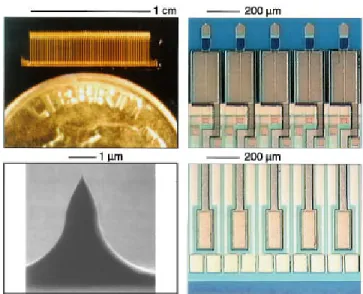
Micrographs showing the array of cantilevers with the corresponding bonding pad layout are shown in Fig. 2. We have fabricated an array of 50 cantilevers that are spaced by 200mm yielding an array spanning 1 cm. Figure 2~a! shows the 1 cm array next to a dime for scale. Figure 2~b! shows a detail of five cantilevers within the array. The piezoresistor and ZnO regions are clearly seen. The two horizontal metal lines running across the device are the piezoresistor and the ZnO ground busses. The three contacts per cantilever ~pi-ezoresistor sensor, ZnO actuator, and tip bias! run vertically down the die to the bonding pads shown in Fig. 2~d!. Each device occupies a horizontal footprint of 200mm, which is the minimum achievable tip-to-tip spacing due to the design limitations on the bonding pads. @The bonding services cur-rently available to us can bond two rows of pads where each row is on a 100 mm period. This was the basis for our con-tact configuration as shown in Fig. 2~d!.# A close up of the integrated tip is shown in Fig. 2~c!. The radius of curvature of these single-crystal silicon tips is generally less than 100 A. This tip was engineered using gas variations in a plasma etch to produce a high aspect ratio profile that is useful for
both imaging and lithography. The tips are covered with a thin film of titanium to enhance the capability for lithogra-phy.
For small arrays of cantilevers it is possible to manually control all aspects of the cantilever’s operation during an imaging or lithography experiment. However, for massively parallel operations, or operation in a scalable system, it is important to have a compact electronic system for automated control. In the piezoresistive/ZnO system, the position of the cantilever arm is detected by microvolt changes in the pi-ezoresistive sensor’s bridge circuit. This voltage is amplified to tens of volts to generate a suitable signal for feedback and analysis. Since the voltage gain is high, special consider-ations need to be given to electronic noise and phase delays in order to create a high-speed, sensitive, electronic system.
FIG. 1. Schematic illustration of the expandable cantilever design with in-tegrated piezoresistive sensor and inin-tegrated ZnO actuator. The perspective view on the left shows the final device, while the exploded view on the right shows the pattern of all of the films in the device.
FIG. 2. ~a! and ~b! An array of cantilevers with integrated actuators and sensors with improved shielding between the actuator and sensor. Part~a! shows an entire array of 50 cantilevers spanning 1 cm next to a dime~for scale!. Part ~b! shows a detail of five of the cantilevers. The cantilevers are spaced by 200mm~c! SEM of a typical integrated single-crystal silicon tip. The radius of curvature is below 10 nm.~d! corresponding electrical contact structure for the cantilevers. There are three leads per device: piezoresistor, ZnO, and tip bias.
FIG. 3. Schematic illustration of the automated parallel high-speed AFM. A computer-controlled PC card contains the electronics to automatically con-trol the operational parameters of the cantilevers shown in Fig. 2~set point, gain, and feedback!. A second computer is used to collect the data and control the scan.
2341
Automation is achieved through computer control of the mi-croscope’s operational parameters: force setpoint, gain, and feedback. A schematic of the automated microscope is shown in Fig. 3. Two computers are used for imaging. One contains the custom electronic PC expansion board and is responsible for monitoring and modifying the cantilevers op-erational parameters. The other computer is responsible for collecting data and controlling the scanner.
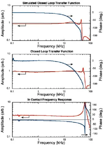
The transfer function of the electronic system is shown in Fig. 4. Figure 4~a! is a simulation of the combined elec-tronic and mechanical system. The cantilever was modeled as a second-order system with a resonance of 50 kHz and a Q of 100. These parameters were determined from the open-loop transfer function of the cantilever when the tip is in contact with a sample@Fig. 4~c!#. The electronic system was modeled using the written specifications of each of the cir-cuit components. Figure 4~b! shows the measured closed-loop response of the cantilever and electronic system. We found excellent agreement between the simulations and the measured data. The primary limitation on bandwidth is due to the resonance of the cantilever. The influence of the elec-tronic phase can be seen in the closed-loop response in the small hump before the peak in the amplitude trace. The
bandwidth of the amplifier chain is measured to be 1.1 MHz and the phase shift at 100 kHz is less than 10°.
A 431 image obtained with the cantilevers and control electronics is shown in Fig. 5. A detail of a memory cell on an integrated circuit chip is shown in Fig. 5~a!. The scan size is just over 100mm3100mm, which is the limit of a con-ventional piezotube. The ZnO actuator is able to track the 2 mm high topography at 1 mm/s. The images do not overlap because the tips are 200mm apart while the scan is only 100 mm. Figure 5~b! shows a parallel image acquired at a scan speed of 4 mm/s. The minimum detectable deflection for this image is less than 5 nm in a 20 kHz bandwidth.
The authors would like to acknowledge Babur Hadimio-glu and Nick Ulman. Support for this work came from DARPA and SRC. S.C.M. and S.R.M. acknowledge support from the Leland T. Edwards fellowship.
1M. Tortonese, H. Yamada, R. C. Barrett, and C. F. Quate, The
Proceed-ings of Transducers ’91~IEEE, Pennington, NJ, 1991!, Publication No.
91 CH2817-5, p. 448.
2S. C. Minne, Ph. Flueckiger, H. T. Soh, and C. F. Quate, J. Vac. Sci. Technol. B 13, 1380~1995!.
3M. Lutwyche, C. Andreoli, G. Binnig, J. Brugger, U. Drechsler, W. Hae-berle, H. Rohrer, H. Rothuizen, and P. Vettiger, Proceedings IEEE Inter-national Workshop on Microelectro Mechanical Systems ~MEMS 98!, Heidelberg, Germany, Jan 25–29, 1998.
4B. W. Chui, T. D. Stowe, T. W. Kenny, H. J. Mamin, B. D. Terris, and D. Rugar, Appl. Phys. Lett. 69, 2767~1996!.
5
R. P. Ried, H. J. Mamin, B. D. Terris, L. S. Fan, and D. Rugar, J. Micro-electromech. Syst. 6, 294~1997!.
6H. P. Lang, R. Berger, C. Andreoli, J. Brugger, M. Despont, P. Vettiger, Ch. Gerber, J. K. Gimzewski, J. P. Ramseyer, E. Meyer, and H. J. Guntherodt, Appl. Phys. Lett. 73, 383~1998!.
7
R. C. Barett and C. F. Quate, J. Vac. Sci. Technol. B 9, 302~1991!. 8H. J. Mamin, H. Birk, P. Wimmer, and D. Rugar, J. Appl. Phys. 75, 161
~1994!.
9S. R. Manalis, S. C. Minne, and C. F. Quate, Appl. Phys. Lett. 68, 871
~1995!.
10
S. R. Manalis, S. C. Minne, A. Atalar, and C. F. Quate, Rev. Sci. Instrum. 67, 3294~1996!.
FIG. 4. ~a! Simulated closed-loop transfer function. Simulation parameters for the cantilever were measured, as shown in part c, and for the electronics were taken from the data sheets.~b! Measured closed-loop transfer function
~cantilever plus electronics!. The bandwidth of the system using a 40° phase
margin is 20 kHz.~c! Open-loop transfer function ~cantilever only! of the cantilever in contact with a smooth sample.
FIG. 5. 431 images of ~a! a memory cell of an integrated circuit and ~b! two-dimensional grating both obtained in parallel with the cantilevers shown in Fig. 2 and the electronics shown in Fig. 3. The bandwidth of the system in 20 kHz, and the sensitivity is less than 5 nm in that band. The tip velocity for the images is 1 and 4 mm/s for parts~a! and ~b!, respectively.