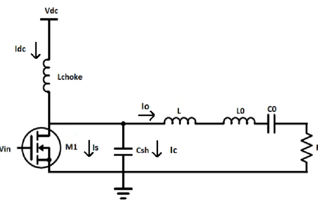
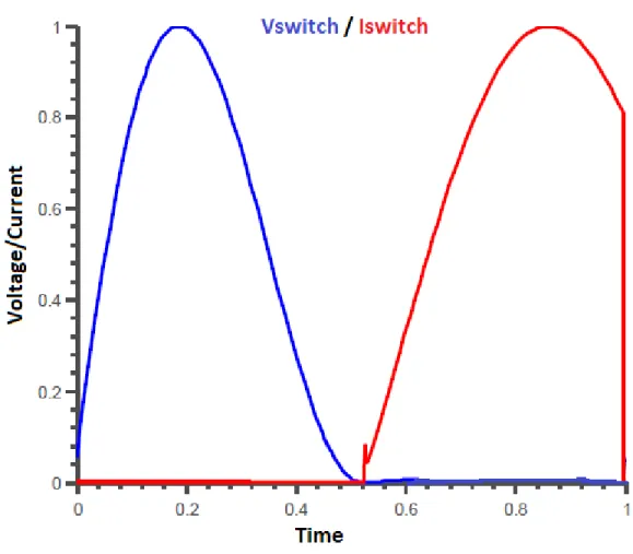
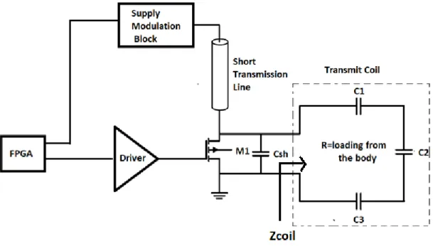
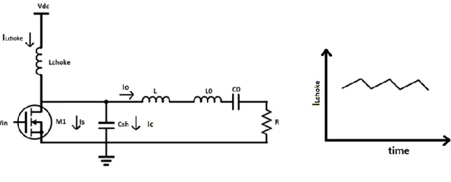
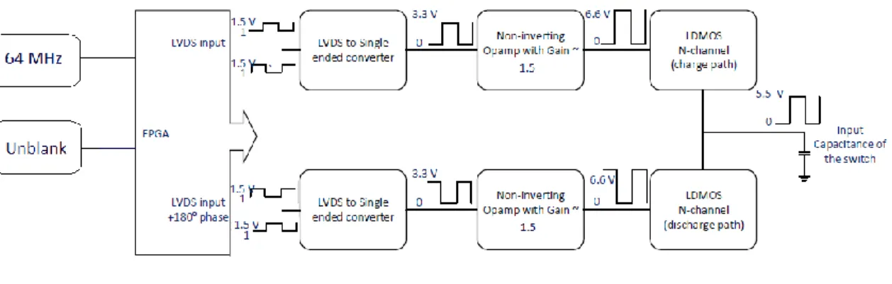
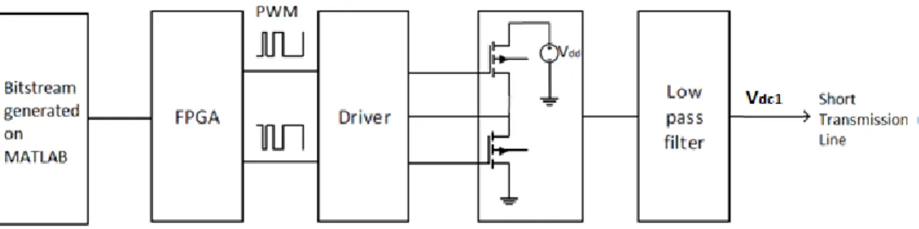
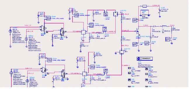
Highly efficient 300 W modified class-E RF amplifiers for 64 MHz transmit array system
Tam metin
Şekil


Benzer Belgeler
In the present work, for the determination of the number of different chemical states of platinum particles in the samples of model Pt/SiO 2 catalysts in their interaction with
In the second chapter we concisely intro- duce some background concepts to gain a clear perspective to the thesis: Jellium Model, Wigner-Seits radius, particle density and
https://www.researchgate.net/publication/5171127 Analyzing the Persistence of Currency Substitution Using a Ratchet Variable : The Turkish Case Article in Emerging Markets
Lower levels of serum high-density lipoprotein cholesterol are associated with a worse Duke treadmill score in men but not in women.. Copyright of Journal of Postgraduate Medicine
In addition to these, relative yield total (RYT) values were calculated for the mixtures. The study showed that the characters studied were significantly influenced by years,
Our findings with dH1fs were applicable to other human fibroblasts, as IMR-90 and MRC-5 cells also showed threefold and sixfold increases in reprogramming efficiency, respectively,
As it is stated, there are six type of shocks in this model. However, since my main aim is to observe the effectiveness of reserve requirements on current account deficit, I will
The resulting tendency of experts to make buy recommendations (indicat- ing predicted stock price increases) was displayed in this study via significant overforecasting
