PROCEEDINGS OF SPIE
SPIEDigitalLibrary.org/conference-proceedings-of-spie
IFVD-based large intermixing
selectivity window process for high
power laser diodes
Seval Arslan, Seval Şahin, Abdullah Demir, Atilla
Aydinli
Seval Arslan, Seval Şahin, Abdullah Demir, Atilla Aydinli, "IFVD-based
large intermixing selectivity window process for high power laser diodes,"
Proc. SPIE 10682, Semiconductor Lasers and Laser Dynamics VIII, 106821S
(9 May 2018); doi: 10.1117/12.2306833
IFVD-based large intermixing selectivity window process for high
power laser diodes
Seval Arslan*
a, Seval Şahin
b, Abdullah Demir
a, Atilla Aydınlı
ca
Dept. of Physics, I.D. Bilkent Univ., Ankara, TURKEY 06800;
bDept. of Physics, Anadolu Univ., Eskişehir, TURKEY;
c
Dept. of Electrical and Electronics Engineering, Uludağ Univ., Bursa, TURKEY 16059
ABSTRACT
Catastrophic optical mirror damage (COMD) is a key issue in semiconductor lasers and it is initiated by facet heating because of optical absorption. To reduce optical absorption, the most promising method is to form non-absorbing mirror structures at the facets by obtaining larger bandgap through impurity-free vacancy disordering (IFVD). To apply an IFVD process while fabricating high-power laser diodes, intermixing window and intermixing suppression regions are needed. Increasing the bandgap difference (ΔE) between these regions improves the laser lifetime. In this report, SrF2
(versus SixO2/SrF2 bilayer) and SiO2 dielectric films are used to suppress and enhance the intermixing, respectively.
However, defects are formed during the annealing process of single layer SrF2 causing detrimental effects on the
semiconductor laser performance. As an alternative method, SixO2/SrF2 bilayer films with a thin SixO2 dielectric layer is
employed to obtain high epitaxial quality during annealing with small penalty on the suppression effect. We demonstrate record large ΔE of 125 meV. Broad area laser diodes were fabricated by the IFVD process. Fabricated high-power semiconductor lasers demonstrated conservation of quantum efficiency with high intermixing selectivity. The differential quantum efficiencies are 81%, 74%, 66% and 46% for as grown, bilayer protected, SrF2 protected and QWI
lasers, respectively. High power laser diodes using bilayer dielectric films outperformed single-layer based approach in terms of the fundamental operational parameters of lasers. Comparable results obtained for the as-grown and annealed bilayer protected lasers promises a novel method to fabricate high power laser diodes with superior performance and reliability.
Keywords: impurity free vacancy disordering, high power laser diodes, catastrophic optical mirror damage.
1. INTRODUCTION
High power semiconductor lasers in the 9xx-nm spectral range have been used in a wide range of industrial applications and, lately, attracted much attention as pumping sources for kW-level fiber lasers and material processing1. Therefore, recent research efforts have concentrated on understanding the limitations and increasing the laser output power of GaAs-based semiconductor lasers2-5. Even though record high output powers have been demonstrated2,4,5, operational
power levels are much lower than the maximum achievable values1. One of the limitations3,5,6 for high laser output
power operation is the catastrophic optical mirror damage (COMD) initiated by facet heating due to optical absorption, which limits the reliable power and lifetime of a single laser emitter6 and, at the system level, increases the cost of
kW-class lasers.
Various facet engineering techniques have been studied to suppress COMD based on laser structure design, regrowth or post-growth7. Post-growth is preferred because it is relatively easier to implement. Quantum well intermixing (QWI),
also called disordering, is one of the common post-growth methods implemented to acquire larger energy bandgap windows near output facet regions to reduce or even eliminate interband absorption in the output window region. QWI involves interdiffusion of the atoms across the QW to modify its material composition and create a larger bandgap. This can be achieved by impurity induced disordering, laser-induced intermixing and impurity-free vacancy disordering (IFVD)7-11. Among these, IFVD has been the most promising intermixing approach since it does not introduce additional
impurities and hence eliminates free carrier absorption losses and, in the ideal case, preserves epitaxial quality.
The IFVD process requires the deposition of a dielectric cap material on the surface of the sample and thermal treatment process ranging from 850 to 950oC. IFVD mechanism involves Ga out-diffusion from the QW in the active region of the
sample to the dielectric cap resulting in the generation of vacancies inside the epitaxial structure. Ga out-diffusion leads primarily to Al-Ga interdiffusion between the GaAs or InGaAs QW and AlGaAs barrier/waveguide layers. The dielectric cap controls the degree of intermixing that can be enhanced or suppressed with the appropriate dielectric material and annealing temperature. For InGaAs, GaAs or AlGaAs QW materials, SiO2 and Si3N4 have been reported to
induce disordering, whereas Si3N4, TiO2 and SrF2 have been commonly used for the suppression of intermixing8,9,12-15.
SiO2 was demonstrated to enhance and suppress intermixing by varying its stoichiometry through modification of flow
rates in plasma enhanced chemical vapor deposition (PECVD) systems16. In high power lasers, it is rare that both the less
deterioration in the suppression region and large intermixing selectivity17-19. In these studies, PECVD and thermal
evaporation films were employed to create IFVD-based non-absorbing windows and suppression in gain regions of InGaAs/AlGaAs QW systems. Intermixing under SiO2 and suppression under SrF2 caps were demonstrated for
GaAs/AlGaAs QW structures. However, SrF2-capped laser devices either suffered from a penalty on operational voltage
(more than 1 V) and slope efficiencies20,21 or some surface damage8 which can distort the reliable operation of devices.
Several studies suggest that the device lifetime of high power laser diodes with a non-absorbing mirror increases with the high selective window (differential blueshift)18,19. Increasing the QWI selectivity reduces the band edge optical
absorption corresponding to increased device lifetime due to improved COMD level. Naito et al. demonstrated stable semiconductor lasers operation of more than 5000 hours at 20W using 100 meV intermixing selectivity between the gain and window region in IFVD process19. Despite widespread reports on IFVD, its application to broad-area laser diodes
have been limited and little have been disclosed on the applied IFVD processes18-20. It is essential to increase ∆E and
obtain high material quality after annealing to realize reliable high-power laser diodes with a long lifetime.
In this work, we report an IFVD method using bilayer dielectric capping and extended time annealing at relatively low annealing temperatures compared to the previous reports8,11,13,16,17,20-22. SiO
2 layer was used for enhanced intermixing
and SixO2/SrF2 bilayer was developed for intermixing suppression. The bilayer capping with thin SixO2 buffer layer is
utilized to keep the epitaxial surface protected against SrF2 induced damage and performance penalties, which was
reported in previous studies8,21,22 and also observed in our work. We demonstrated high selectivity in QWI achieving
bandgap difference of ∆λ = 75 nm (∆E = 125 meV) by 6-minute annealing at 880oC for a GaAs-based laser structure with a negligible shift of the bandgap in the suppression region. PL wavelength shift from around 900 nm for as-grown InGaAs QW to 825 nm for IFVD induced InGaAlAs QW sample indicated that intermixing reached saturation since further wavelength shift could not be realized by increasing annealing time or temperature. As an application of this IFVD procedure, we fabricated high power broad-area semiconductor lasers emitting at 915 nm demonstrating insignificant penalty on the laser threshold current, slope efficiency, and operating voltage.
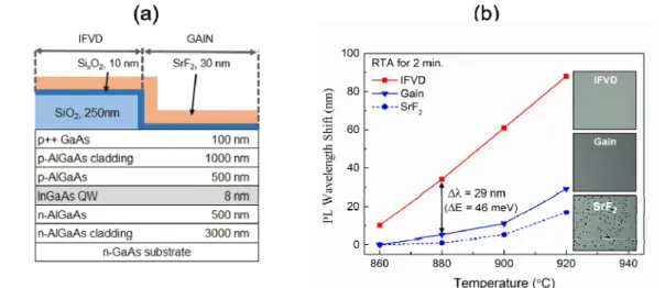
2. EXPERIMENTAL
Fig.1a shows the laser structure and dielectric films used in this study for the IFVD experiments. Separate confinement heterostructure with single InGaAs QW (ground state λPL~900 nm at RT) was grown on an n-GaAs substrate by
metalorganic chemical vapor deposition (MOCVD). 8 nm InGaAs QW is sandwiched between a 500-nm n-AlGaAs and a 500-nm p-AlGaAs waveguides. Cladding layers are composed of a 3000-nm n-AlGaAs and a 1000 nm p-AlGaAs layers. There is a 100 nm GaAs contact layer at top of the epitaxial structure. The doping level within ±300 nm around the QW was kept below 5x1016cm-3 with low diffusion constant dopants (i.e. C and Si) so that the effect of doping on
QWI is negligible. Onto this laser structure, SiO2 and SixO2 were deposited by PECVD, and SrF2 was deposited by
thermal evaporation. For SiO2 deposition, SiH4 (2% in He) and N2O flow rates were set at 30 sccm and 1000 sccm,
respectively. For SixO2 deposition, SiH4 (2% in He) and N2O flow rates were set at 320 sccm and 800 sccm, respectively.
Both oxides were deposited at 300⁰C with an rf power of 20 W and 1 Torr base pressure. SrF2 was deposited at a rate of
1.7 A/s under 5x10⁻⁶ Torr. The refractive index and thickness of the deposited films were characterized by spectroscopic
ellipsometer and refractive indices were measured as 1.46 for SiO2, 1.57 for SixO2 and 1.38 for SrF2 at 633nm. The
thicknesses of the deposited dielectric layers were 250, 10 and 30 nm for SiO2, SixO2 and SrF2, respectively. Rapid
thermal annealing (RTA) was carried out in nitrogen ambient. Samples capped with GaAs wafers to prevent As out-diffusion during the annealing process. For PL measurements, dielectric layers were removed and around 1 µm of the top epitaxial layer was etched off. Oxides and SrF2 were etched in HF and HCl based solutions, respectively. For PL
measurements, Ar+ laser of λ=514.5 nm was used as the excitation source and luminescence was collected by a
amount of QWI after RTA, room temperature PL measurements were performed, and linewidth and integrated intensity were analyzed.
We studied the non-absorbing window formation process for laser diodes by defining two distinct regions, where the first one is for IFVD window (250 nm SiO2) to intermix the QW and the second is for protected gain region (30 nm SrF2
or 10nm/ 30nm SixO2/SrF2) to suppress the intermixing of the QW. After deposition of 250 nm SiO2 intermixing
dielectric, a region was masked by a photoresist (PR) and unprotected dielectric was removed by using buffered oxide etch (BOE; NH4F: HF, 7:1). PR was stripped off with acetone followed by plasma descum step to eliminate residues. To
protect the surface against SrF2 induced damage, 10 nm thick SixO2 protection layer was deposited on the whole sample
and followed by thermal evaporation of 30 nm thick SrF2. Before the deposition of every dielectric layer, the samples
were cleaned by using dilute HCl (H2O: HCl, 10:1). QWI under various temperatures ranging from 860 to 920oC for 2
minutes were performed.
We also investigated the effect of extended time annealing on the intermixing selectivity enhancement and PL recovery. To study the intermixing selectivity and crystal quality improvement effect, extended time of 4 and 6 min. were employed at 880oC.
Finally, ridge waveguide high power laser diodes were fabricated with traditional and IFVD processed structures. IFVD process with intermixing (250nm-SiO2) and suppression (10nm-SixO2/30nm-SrF2) waveguides were formed by using the
developed process. Traditional lasers also fabricated in parallel for comparison. Ridge waveguides were fabricated by using wet etch solution of H3PO4:H2O2:H2O. A 200nm thick Si3N4 layer was deposited to act as an electrical insulator
and current injection windows were opened on top of the ridge waveguides. Ti/Pt/Au by e-beam and GeAu/Ni/Au by thermal evaporation were deposited to form p- and n-contacts, respectively. This was followed by alloying the ohmic contacts in RTA at 420oC for 1 min. The fabricated lasers were cleaved and tested epi-side up under continuous wave (CW) operation current at room temperature.
3. RESULTS AND DISCUSSIONS
Fig. 1b demonstrates the PL wavelength shifts of IFVD, gain regions and SrF2-only relative to as grown structure after 2
minutes of RTA at various annealing temperatures of 860, 880, 900 and 920 °C. PL wavelength shifts to shorter wavelengths as the dielectric layer thickness increases22. For both SiO2 and SixO2 layers, we found that thicknesses
above 250 nm do not provide additional QWI wavelength shift with the increase of their thickness. The deposition recipe for silicon-rich oxide, i.e. SixO2, was developed to yield smaller wavelength shifts compared to SiO2 as described in
reference17. SrF
2 deposited samples clearly show that the QWI is suppressed with respect to the oxide capped case. At
880oC, a negligible shift was observed in the SrF2 capped region. However, the surface damage was clearly detected
after removal of the dielectric as shown by optical microscope images in the inset of Fig.1b in line with the former observations in the literature8,20-23. In comparing the results for the gain region and SrF
2, the effectiveness of bilayer in
protecting the surface against damage and obtaining similar PL wavelength shifts are clearly demonstrated. For samples annealed at 880oC for 2 minutes, there is a small penalty in wavelength shift difference that reduces to 29 nm for SixO2/SrF2 down from 33 nm for the SrF2-only sample.
0
- RTA for 2 min.
-- IFVD
-v-
Gain (a) (b) 860 880 900 Temperature ( °C) 920i
0 IFVD SixO2i 10 nm:'Mt
Ì
S102, 250nm p ++GaAs p- AIGaAs cladding p-AIGaAs Inn". Anmitt GAI N -SrF2, 30 nm 100 nm 1000 nm 500 nm Onrn(b)
100 80 60 40RTA for 2 min. IFVD
--e -Gain
-- -- SrF2
n)L = 2Q nm
Gain
Figure 1 (a) Schematic of IFVD (QWI enhanced) and gain (QWI suppressed) configuration used in this study (b) PL peak wavelength shift under annealing conditionsof 860 to 920oC for 2 minutes.
Fig. 2 shows the ground state full-width at half-maximum (FWHM) and integrated PL intensity for 2 min. RTA process as a function of the RTA temperature. There is no substantial change in FWHM of the intermixed and suppressed regions indicating that the QW thickness homogeneity is preserved both in IFVD and gain sections. The PL FWHM remains largely unaffected but integrated PL intensity in IFVD region reduces with the temperature that also correlates with the amount of wavelength shift. PL intensity reduction might occur due to the carrier escape from the QW becoming shallower with higher temperature as well as due to enhanced non-radiative e-h recombination through deep interband levels created by Ga-vacancies during IFVD22. For the gain region, FWHM remains mainly unaffected but
integrated PL intensity increases slightly with temperature, which contrasts with that of the IFVD region. The intensity increase was observed in previous studies and attributed to SrF2 induced surface roughness causing larger PL
extraction22, but it is not anticipated to contribute to the results of our study since the surface quality was improved
dramatically by the bilayer deposition technique. The slight intensity increase in the gain region with temperature might be due to the reduction of point defects at higher temperatures even with larger blue shifts. However, this would mean intermixing suppression process is not optimum in the applied range of annealing temperatures with minimum suppression wavelength shift, e.g. 860 or 880oC, since integrated PL intensity is lower in this range.
Figure 2. FWHM and integrated PL intensity of IFVD and gain regions under annealing conditions of 860 to 920oC for 2 min.
100 80 60 40 20 0 RTA at 880°C IFVD - -v-Gain 75 nm (AE= 125 meV) (a) 2 4
Annealing time (min.)
= 20 15 C d " 10 a J 5 a
^
z m 4 d Ñ 3 ÿc 2 C J 1 o-o - RTA at 880°C -a- IFVD -a-Gain (a) 2 4Annealing time (min.)
6
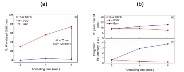
Fig. 3a shows the PL wavelength shifts results of IFVD and gain region for extended time RTA process at 880 °C. It demonstrates that the degree of intermixing selectivity increases with the annealing time mainly due to the wavelength shifts of the IFVD regions because gain region wavelength stays almost constant as the time increases. Maximum ΔE was obtained from the 6 min. RTA process. When the RTA duration is increased above 6 min., the wavelength of the IFVD will not shift, however that of the gain region starts to shift and it is not accepted for high power laser diodes. Intermixing selectivity of 75 nm (125 meV) was achieved for 6 min. annealing.
Fig. 3b summarizes the ground state FWHM and integrated PL intensity change with extended time RTA process. A small decrease of FWHM in IFVD region is possibly due to high energy tail of the shallower confinement with larger QWI blueshift. A slight increase of the gain region FWHM with annealing time is likely to be higher order state contribution because of the smaller QW state spacing as described in Fig. 3b. Nearly constant FWHM of the gain region indicates that the QW thickness homogeneity is preserved. Slight integrated intensity decline of the IFVD region with further annealing and increased intermixing follows a similar trend as in fig. 2, which agrees with the increase of non-radiative recombination centers due to Ga-vacancies. Gain region improvement by increased annealing cycles is obvious with substantial PL intensity increase. Compared to 2-minute annealing, integrated intensity is six times higher at 6-minute RTA suggesting a significant improvement in the material quality.
Figure 3. (a) PL peak wavelength shift and (b) FWHM and integrated PL intensity of IFVD and gain regions for extended time annealing at 880oC.
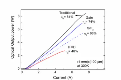
In Fig. 4 compares the performance of the RTA processed lasers with traditional lasers, which were fabricated following the process described above. IFVd were performed at 880 °C for 4 min. At this condition, the wavelength shift between the gain and IFVD window region is ~45 nm (70 meV) (is not shown). The differential quantum efficiencies are 81%, 74%, 66% and 46% for traditional, gain, SrF2 and IFVD lasers, respectively. The differential quantum efficiency of the
SrF2 is much distorted due to the defects inside this laser. However, gain laser overcomes this problem with slight
penalty in lasing wavelength and the differential quantum efficiency of this laser became close to that of the traditional laser.
8F Traditional nd =81% Gain { .. =66/ I o d= /4% SrF2 p at 300K
7
Current (A)ó
4r/
nIF4Do/ 1 CL 20
(4 mm\wino..m)Figure 4. (a) Comparison of the optical output power of RTA processed and traditional lasers with respect to operational current.
4. SUMMARY
In summary, we have demonstrated a highly selective QWI technique for InGaAs QW structures. SiO2 was used for
intermixing enhancement and employing bilayer dielectrics of SixO2/SrF2 provided both excellent surface morphology
and intermixing suppression. Extended time annealing was presented to enhance the QWI selectivity and restore the material quality of the structure. Large QWI blueshift difference of 75 nm (= 125 meV) was achieved by 6-minute annealing at 880oC with a high degree of reproducibility. To verify the device fabrication compatibility of the developed method, we fabricated high power broad-area semiconductor lasers with as-grown and bilayer protected annealed samples. Our results indicate that the bilayer method does not cause any significant deterioration on the laser threshold current, slope efficiency and operating voltage of broad area laser diodes.
The QWI process is suitable and can be exploited for the monolithic integration of passive and active devices such as low-loss waveguides, modulators and distributed Bragg reflectors (DBR) integrated with widely tunable semiconductor lasers and photodetectors24,25. Low-loss waveguides can be introduced for DBR sections to reduce direct interband
absorption losses26. The amount of differential blueshift and material quality are key for performance enhancements in
these applications for photonics integrated circuits. Currently, semiconductor lasers are the most efficient high-power output devices, but their performance and output power can be further boosted by IFVD window technique.
Acknowledgements
The financial support of Ermaksan A.Ş. is gratefully acknowledged.
REFERENCES
[1] Zucker, E. et al., “Advancements in laser diode chip and packaging technologies for application in kW-class fiber laser pumping,” Proc. of SPIE 8965, 896507 (2014).
[2] Petrescu-Prahova, I. B. et al., “High d/gamma values in diode laser structures for very high power,” Proc. of SPIE 7198, 71981I (2009).
[3] Wenzel, H., Crump, P., Pietrzak, A., Wang, X., Erbert, G., and Tränkle, G., “Theoretical and experimental investigations of the limits to the maximum output power of laser diodes,” New J. Phys., 12 (2010).
[4] Demir, A., Peters, M., Duesterberg, R., Rossin, V., and Zucker, E., “29.5W continuous wave output from 100 μm wide laser diode,” Proc. of SPIE 9348, 93480G (2015).
[5] Demir, A., Peters, M., Duesterberg, R., Rossin, V., and Zucker, E., “Semiconductor Laser Power Enhancement by Control of Gain and Power Profiles,” IEEE Photon. Technol. Lett. 27 (2015).
[6] Hempel, M. et al., "Catastrophic optical damage at front and rear facets of diode lasers," Appl. Phys. Lett. 97 (2010).
[7] Epperlein, P. W., “Semiconductor Laser Engineering, Reliability and Diagnostics: A Practical Approach to High Power and Single Mode Devices,” UK: Wiley, (2013).
[8] Ooi, B. S. et al., “Selective quantum-well intermixing in GaAs-AlGaAs structures using impurity-free vacancy diffusion,” IEEE J. Quantum Electron. 33 (1997).
[9] Furtado, M. T., Loural, M. S. S., Sato, E. A., and Sacilotti, M. A., “Impurity-induced disorder in strained InGaAs/GaAs quantum wells by Zn diffusion and thermal annealing”Semicond. Sci. Technol. 7 (1992).
[10] Byun, Y. T., Jhon, Y. M., Kim, S. H., “Blue shifting of Ion implanted InGaAs/InGaAsP multiple quantum well structures using two-step rapid temperature annealing process,” Jpn J Appl Phys, 50 (2011).
[11] Du, S. C., Fu, L., Tan, H. H., Jagadish, C.,, “Investigations of impurity-free vacancy disordering in
(Al)InGaAs(P)/InGaAs quantum wells”Semicond. Sci. Technol. 25 (2010).
[12] Yu, J. S., Song, J. D., Lee, Y. T., Lim, H.,, “Influence of dielectric deposition parameters on the In0.2Ga0.8As/GaAs
quantum well intermixing by impurity-free vacancy disordering,” J. Appl. Phys. 92 (2002).
[13] Gareso, P. L., Buda, M., Fu, L., Tan, H. H., Jagadish, C., “Influence of SiO2 and TiO2 dielectric layers on the atomic
intermixing of InxGa1−xAs/InP quantum well structures,”Semicond. Sci. Technol. 22 (2007).
[14] Gontijo, I., Krauss, T., Marsh, J. H., Delarue, R. M., “Postgrowth control of GaAs/AlGaAs quantum well shapes by impurity-free vacancy diffusion,” IEEEJ Quantum Electron. 30 (1994).
[15] Kahraman, A., Gür, E., and Aydınlı, A., “Impurity-free quantum well intermixing for large optical cavity high-power laser diode structures,” Semicond. Sci. Technol. 31 (2016).
[16] Yu, J. S., Song, J. D., Lee, Y. T., and Lim, H., “Fabrication of multi-wavelength In0.2Ga0.8As/GaAs multiple quantum well laser diodes by area-selective impurity-free vacancy disordering using SiOx capping layers with different stoichiometries,” Appl. Phys A: Mater. Sci. Process. 80 (2005).
[17] Morita, T. et al., “High-Efficient and Reliable Broad-Area Laser Diodes With a Window Structure,” IEEE J. Quantum Electron. 19 (2013).
[18] Naito, H. et al., "Long-Term Reliability of 915-nm Broad-Area Laser Diodes Under 20-W CW Operation," IEEE Photon. Technol. Lett. 27 (2015).
[19] Taniguchi, H. et al., "25-W 915-nm Lasers With Window Structure Fabricated by Impurity-Free Vacancy Disordering (IFVD)," IEEE J. Selec. Top. Quantum Electron. 13 (2007).
[20] Hofstetter, D., Zappe, H. P., Epler, J. E., and Riel, P., “Multiple wavelength Fabry–Pérot lasers fabricated by vacancy enhanced quantum well disordering,” Appl. Phys. Lett. 67 (1995)
[21] Hofstetter, D., Maisenholder, B., and Zappe, H. P., “Quantum-Well Intermixing for Fabrication of Lasers and Photonic IntegratedCircuits,” IEEE J. Sel. Top. Quantum Electron. 4 (1998).
[22] Shimada, N., Fukumoto, Y., Uemukai, T., Suhara, T., Nishihara, H., Larsson, A., “Monolithic integration of laser and passive elements using selective QW disordering by RTA with SiO2 caps of different thichnesses,” IEEE J.
Selec. Top. Quantum Electron. 7 (2001).
[23] Hongpinyo, V. et al., “Intermixing of InGaAs/GaAs Quantum Well Using Multiple Cycles Annealing,” IEEE Photonics Global Conference at Singapore (IPGC), 1 (2008).
[24] Bryce, A. C., Camacho, F., Cusumano, P., and Marsh, J. H., “CW and Mode-Locked Integrated Extended Cavity Lasers Fabricated Using Impurity Free Vacancy Disordering,” IEEE J. Sel. Top. Quantum Electron. 3 (1997). [25] Zhang, X., He, J. J., Liu, N., and Dubowski, J. J., “Carrier-induced fast wavelength switching in tunable V-cavity
laser with quantum well intermixed tuning section,” Opt. Express 23 (2015).
[26] Hou, L., Haji, M., Dylewicz, R., Qiu, B., and Bryce, A. C., “10-GHz Mode-Locked Extended Cavity Laser Integrated With Surface-Etched DBR Fabricated by Quantum-Well Intermixing,” IEEE Photon. Technol. Lett 23 (2011).