www.elsevier.nlrlocatersna
Integration of through-wafer interconnects with a two-dimensional
cantilever array
E.M. Chow
), H.T. Soh, H.C. Lee, J.D. Adams, S.C. Minne, G. Yaralioglu, A. Atalar,
C.F. Quate, T.W. Kenny
Ginzton Laboratory, Stanford UniÕersity, South Box U, Stanford, CA 94305-4085, USA Received 7 June 1999; received in revised form 4 November 1999; accepted 10 November 1999
Abstract
Ž .
High-density through-wafer interconnects are incorporated in a two-dimensional 2D micromachined cantilever array. The design addresses alignment and density issues associated with 2D arrays. Each cantilever has piezoresistive deflection sensors and high-aspect ratio silicon tips. The fabrication process and array operation are described. The integration of cantilevers, tips, and interconnects enables operation of a high-density 2D scanning probe array over large areas. q 2000 Elsevier Science S.A. All rights reserved.
Keywords: Sensor array; Scanning probe microscope; Through-wafer electrical interconnect; Piezoresistive silicon cantilever
1. Introduction
The ability to fabricate small through-wafer electrical interconnections has broad applications for integrated cir-cuits and micromachined devices. Semiconductor micro-fabrication generally places sensors and integrated circuits on only one side of a silicon wafer. With bulk wafer etching techniques, connections between both sides of the wafer can be made, enabling more complicated and com-pact structures. Some of the many examples include
inter-Ž .
connects in integrated circuits, three-dimensional 3D
Ž .
packaging e.g., stacking , and fabrication of 3D electrical
w x
and MEMS structures 1–6 . Small through-wafer inter-connects particularly benefit dense arrays of microfabri-cated sensors, such as ultrasound transducer arrays for imaging and diode arrays for detecting charged particles and X-rays, as they minimize nonsensing area and thus
w x
enhance performance 7,8 . In this work, we focus on a
)
Corresponding author. Tel.: q1-650-723-2279; fax: q1-650-725-7509.
Ž .
E-mail address: [email protected] E.M. Chow .
Ž .
versatile and useful sensor format: two-dimensional 2D arrays of force sensing cantilevers.
Scanning probe devices, such as an atomic force
micro-Ž .
scope AFM , take advantage of high spatial resolution and high force resolution to make significant contributions in a variety of fields. The commercially available AFM can typically measure piconewtons of force, with angstrom vertical resolution and nanometer horizontal resolution. Its ability to operate in water and at atmospheric pressures,
Ž .
unlike scanning electron microscopes SEM , has led to numerous biological imaging and force measurement
ap-w x
plications 9,10 . In lithography, arguably the most critical technology for the integrated circuit industry, scanning
˚
probes have demonstrated 300-A resolution, with a wider
w x
process latitude than electron beam techniques 11 . Metal-oxide semiconductor transistors with 100-nm gate lengths have been demonstrated using scanning probe
w x
lithography 12 . Scanning probe devices using localized heating can achieve 400 Gbitsrin.2 data storage densities; an order of magnitude greater than the paramagnetic limit
w x
which ultimately limits magnetic data storage 13 . While the sensitivity of these techniques is most impressive, throughput and sensing area are hindered by their reliance on serial scanning. The ability to fabricate large, densely packed, 2D arrays of sensors would address this problem,
0924-4247r00r$ - see front matter q 2000 Elsevier Science S.A. All rights reserved.
Ž .
as arrays increase signal throughput without sacrificing the spatial sensitivity of the individual sensor.
One important issue for 2D arrays of scanning probes is
Ž .
alignment. Linear 1D cantilever probe arrays have been demonstrated for cantilevers operating at a nominal 158
w x
angle relative to the sample surface 14,15 . This arrange-ment allows access to wire bonds on the tip side of the wafer without interfering with tip to sample alignment
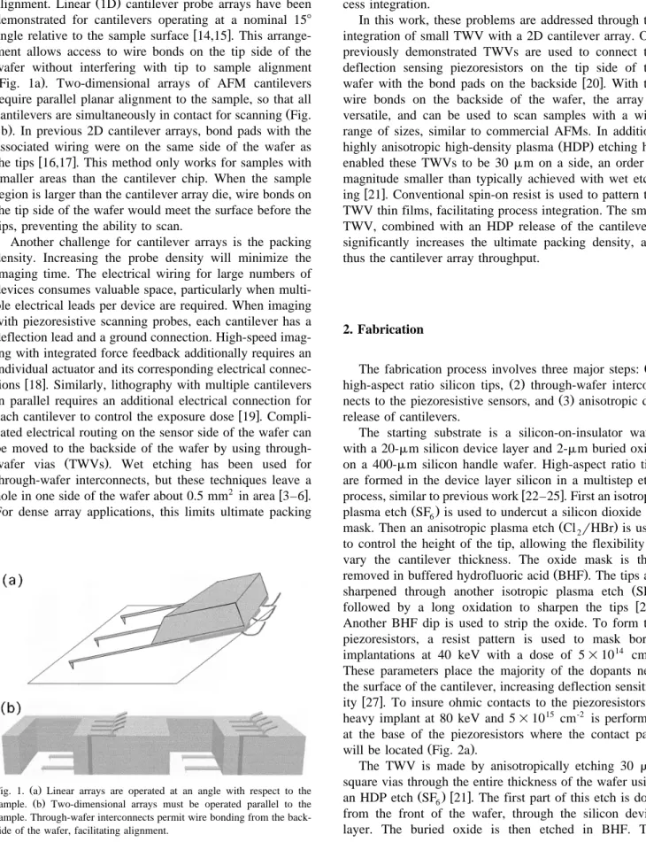
ŽFig. 1a . Two-dimensional arrays of AFM cantilevers.
require parallel planar alignment to the sample, so that all
Ž
cantilevers are simultaneously in contact for scanning Fig.
.
1b . In previous 2D cantilever arrays, bond pads with the associated wiring were on the same side of the wafer as
w x
the tips 16,17 . This method only works for samples with smaller areas than the cantilever chip. When the sample region is larger than the cantilever array die, wire bonds on the tip side of the wafer would meet the surface before the tips, preventing the ability to scan.
Another challenge for cantilever arrays is the packing density. Increasing the probe density will minimize the imaging time. The electrical wiring for large numbers of devices consumes valuable space, particularly when multi-ple electrical leads per device are required. When imaging with piezoresistive scanning probes, each cantilever has a deflection lead and a ground connection. High-speed imag-ing with integrated force feedback additionally requires an individual actuator and its corresponding electrical
connec-w x
tions 18 . Similarly, lithography with multiple cantilevers in parallel requires an additional electrical connection for
w x
each cantilever to control the exposure dose 19 . Compli-cated electrical routing on the sensor side of the wafer can be moved to the backside of the wafer by using
through-Ž .
wafer vias TWVs . Wet etching has been used for
through-wafer interconnects, but these techniques leave a
2 w x
hole in one side of the wafer about 0.5 mm in area 3–6 . For dense array applications, this limits ultimate packing
Ž .
Fig. 1. a Linear arrays are operated at an angle with respect to the
Ž .
sample. b Two-dimensional arrays must be operated parallel to the sample. Through-wafer interconnects permit wire bonding from the back-side of the wafer, facilitating alignment.
density and layout flexibility. Furthermore, lithography over such 3D topography typically requires electrode-posited resist or shadow masking, which complicate pro-cess integration.
In this work, these problems are addressed through the integration of small TWV with a 2D cantilever array. Our previously demonstrated TWVs are used to connect the deflection sensing piezoresistors on the tip side of the
w x
wafer with the bond pads on the backside 20 . With the wire bonds on the backside of the wafer, the array is versatile, and can be used to scan samples with a wide range of sizes, similar to commercial AFMs. In addition,
Ž .
highly anisotropic high-density plasma HDP etching has enabled these TWVs to be 30 mm on a side, an order of magnitude smaller than typically achieved with wet
etch-w x
ing 21 . Conventional spin-on resist is used to pattern the TWV thin films, facilitating process integration. The small TWV, combined with an HDP release of the cantilevers, significantly increases the ultimate packing density, and thus the cantilever array throughput.
2. Fabrication
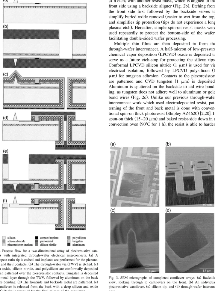
Ž .
The fabrication process involves three major steps: 1
Ž .
high-aspect ratio silicon tips, 2 through-wafer
intercon-Ž .
nects to the piezoresistive sensors, and 3 anisotropic dry release of cantilevers.
The starting substrate is a silicon-on-insulator wafer with a 20-mm silicon device layer and 2-mm buried oxide on a 400-mm silicon handle wafer. High-aspect ratio tips are formed in the device layer silicon in a multistep etch
w x
process, similar to previous work 22–25 . First an isotropic
Ž .
plasma etch SF6 is used to undercut a silicon dioxide tip
Ž .
mask. Then an anisotropic plasma etch Cl rHBr is used2 to control the height of the tip, allowing the flexibility to vary the cantilever thickness. The oxide mask is then
Ž .
removed in buffered hydrofluoric acid BHF . The tips are
Ž .
sharpened through another isotropic plasma etch SF6
w x
followed by a long oxidation to sharpen the tips 26 . Another BHF dip is used to strip the oxide. To form the piezoresistors, a resist pattern is used to mask boron implantations at 40 keV with a dose of 5 = 1014 cm-2. These parameters place the majority of the dopants near the surface of the cantilever, increasing deflection
sensitiv-w x
ity 27 . To insure ohmic contacts to the piezoresistors, a heavy implant at 80 keV and 5 = 1015 cm-2 is performed at the base of the piezoresistors where the contact pads
Ž .
will be located Fig. 2a .
The TWV is made by anisotropically etching 30 mm square vias through the entire thickness of the wafer using
Ž . w x
an HDP etch SF6 21 . The first part of this etch is done from the front of the wafer, through the silicon device layer. The buried oxide is then etched in BHF. The
Fig. 2. Process flow for a two-dimensional array of piezoresistive
can-Ž .
tilevers with integrated through-wafer electrical interconnects. a A high-aspect ratio tip is etched and implants are performed for the
piezore-Ž . Ž . Ž .
sistors and their contacts. b The through-wafer via TWV is etched. c Silicon oxide, silicon nitride, and polysilicon are conformally deposited and then patterned over the piezoresistor contacts. Tungsten is deposited as the metal layer through the TWV, followed by aluminum on the back
Ž . Ž .
for wire bonding. d The frontside and backside metal are patterned. e The cantilever is released from the back with a deep silicon and oxide
Ž .
etch. f Resist is removed for the final release of the cantilever.
majority of the TWV is etched from the back of the wafer
Ž4 h etch with another resist mask, which is aligned to the.
Ž .
front side using a backside aligner Fig. 2b . Etching from the front side first followed by the backside serves to
Ž .
simplify buried oxide removal easier to wet from the top
Ž
and simplifies tip protection tips do not experience a long
.
plasma etch . Hereafter, simple spin-on resist masks were used repeatedly to protect the bottom-side of the wafer, facilitating double-sided wafer processing.
Multiple thin films are then deposited to form the through-wafer interconnect. A half-micron of low-pressure
Ž .
chemical vapor deposition LPCVD oxide is deposited to serve as a future etch-stop for protecting the silicon tips.
Ž .
Conformal LPCVD silicon nitride 1 mm is used for via
Ž
electrical isolation, followed by LPCVD polysilicon 1
.
mm for tungsten adhesion. Contacts to the piezoresistors
Ž .
are patterned and CVD tungsten 1 mm is deposited.
Aluminum is sputtered on the backside to aid wire bond-ing, as tungsten does not adhere well to aluminum or gold
Ž .
bond wires Fig. 2c . Unlike our previous through-wafer interconnect work which used electrodeposited resist, pat-terning of the front and back metal is done with
conven-Ž . w x
tional spin-on thick photoresist Shipley AZ4620 2,20 . If
Ž .
spun-on thick 15–20 mm and baked resist-side down in a
Ž .
convection oven 908C for 1 h , the resist is able to harden
Ž .
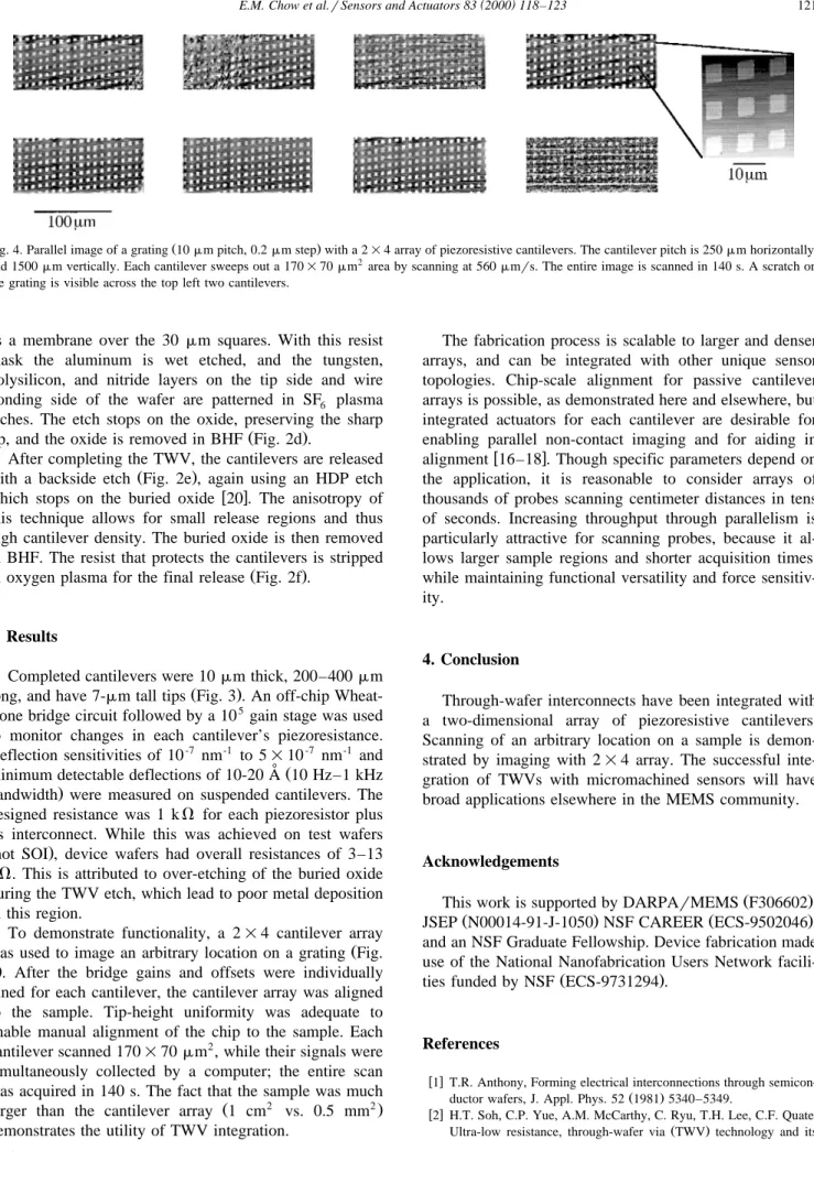
Fig. 3. SEM micrographs of completed cantilever arrays. a Backside
Ž .
view, looking through to cantilevers on the front. b An individual
Ž . Ž .
piezoresistive cantilever, c silicon tip, and d through-wafer intercon-nect.
Ž .
Fig. 4. Parallel image of a grating 10 mm pitch, 0.2 mm step with a 2 = 4 array of piezoresistive cantilevers. The cantilever pitch is 250 mm horizontally, and 1500 mm vertically. Each cantilever sweeps out a 170 = 70 mm2area by scanning at 560 mmrs. The entire image is scanned in 140 s. A scratch on
the grating is visible across the top left two cantilevers.
as a membrane over the 30 mm squares. With this resist mask the aluminum is wet etched, and the tungsten, polysilicon, and nitride layers on the tip side and wire bonding side of the wafer are patterned in SF6 plasma etches. The etch stops on the oxide, preserving the sharp
Ž .
tip, and the oxide is removed in BHF Fig. 2d .
After completing the TWV, the cantilevers are released
Ž .
with a backside etch Fig. 2e , again using an HDP etch
w x
which stops on the buried oxide 20 . The anisotropy of this technique allows for small release regions and thus high cantilever density. The buried oxide is then removed in BHF. The resist that protects the cantilevers is stripped
Ž .
in oxygen plasma for the final release Fig. 2f .
3. Results
Completed cantilevers were 10 mm thick, 200–400 mm
Ž .
long, and have 7-mm tall tips Fig. 3 . An off-chip Wheat-stone bridge circuit followed by a 105gain stage was used to monitor changes in each cantilever’s piezoresistance. Deflection sensitivities of 10-7 nm-1 to 5 = 10-7 nm-1 and
˚
Žminimum detectable deflections of 10-20 A 10 Hz–1 kHz
.
bandwidth were measured on suspended cantilevers. The designed resistance was 1 k V for each piezoresistor plus its interconnect. While this was achieved on test wafers
Žnot SOI , device wafers had overall resistances of 3–13.
k V. This is attributed to over-etching of the buried oxide during the TWV etch, which lead to poor metal deposition in this region.
To demonstrate functionality, a 2 = 4 cantilever array
Ž
was used to image an arbitrary location on a grating Fig.
.
4 . After the bridge gains and offsets were individually tuned for each cantilever, the cantilever array was aligned to the sample. Tip-height uniformity was adequate to enable manual alignment of the chip to the sample. Each cantilever scanned 170 = 70 mm2, while their signals were simultaneously collected by a computer; the entire scan was acquired in 140 s. The fact that the sample was much
Ž 2 2.
larger than the cantilever array 1 cm vs. 0.5 mm
demonstrates the utility of TWV integration.
The fabrication process is scalable to larger and denser arrays, and can be integrated with other unique sensor topologies. Chip-scale alignment for passive cantilever arrays is possible, as demonstrated here and elsewhere, but integrated actuators for each cantilever are desirable for enabling parallel non-contact imaging and for aiding in
w x
alignment 16–18 . Though specific parameters depend on the application, it is reasonable to consider arrays of thousands of probes scanning centimeter distances in tens of seconds. Increasing throughput through parallelism is particularly attractive for scanning probes, because it al-lows larger sample regions and shorter acquisition times, while maintaining functional versatility and force sensitiv-ity.
4. Conclusion
Through-wafer interconnects have been integrated with a two-dimensional array of piezoresistive cantilevers. Scanning of an arbitrary location on a sample is demon-strated by imaging with 2 = 4 array. The successful inte-gration of TWVs with micromachined sensors will have broad applications elsewhere in the MEMS community.
Acknowledgements
Ž .
This work is supported by DARPArMEMS F306602 ,
Ž . Ž .
JSEP N00014-91-J-1050 NSF CAREER ECS-9502046 , and an NSF Graduate Fellowship. Device fabrication made use of the National Nanofabrication Users Network
facili-Ž .
ties funded by NSF ECS-9731294 .
References
w x1 T.R. Anthony, Forming electrical interconnections through semicon-Ž .
ductor wafers, J. Appl. Phys. 52 1981 5340–5349.
w x2 H.T. Soh, C.P. Yue, A.M. McCarthy, C. Ryu, T.H. Lee, C.F. Quate,
Ž .
applications in three dimensional structures in silicon, in: Interna-tional Conference on Solid State Devices and Materials, Hiroshima, Japan, Sept. 7–10,1998, pp. 284–285.
w x3 S. Linder, H. Baltes, F. Gnaedinger, E. Doering, Fabrication
tech-nology for wafer through-hole interconnections and three-dimen-sional stack of chips and wafers, in: Proc. IEEE Micro Electro Mech. Systems, Oiso, Japan,1994, pp. 349–354.
w x4 M. Heschel, J.F. Kuhmann, S. Boustra, Stacking technology for a
space constrained microsystem, J. Intell. Mater. Syst. Struct. 9
Ž1998 749–754..
w x5 C. Christensen, P. Kersten, S. Henke, S. Bouwstra, Wafer
through-hole interconnections with high vertical wiring densities, IEEE
Ž .
Trans. Compon., Packag., Manuf. Technol., Part A 19 1996 516– 522.
w x6 G.J. Burger, E.J.T. Smulders, J.W. Berenschot, T.S.J. Lammerink,
J.H.J. Fluitman, S. Imai, High-resolution shadow-mask patterning in deep holes and its application to an electrical wafer feed-through,
Ž .
Sens. Actuators, A 54 1996 669–673.
w x7 C. Kenney, S. Parker, J. Segal, C. Storment, Silicon detectors with
3D electrode arrays: fabrication and initial test results, IEEE Trans.
Ž .
Nucl. Sci. 46 1999 1224–1236.
w x8 X.C. Jin, S. Calmes, C.H. Cheng, F.L. Degertekin, B.T.
Khuri-Yakub, Micromachined capacitive ultrasonic immersion transducer array, in: Tech. Digest, 10th Int. Conf. Solid-State Sensors and
Ž .
Actuators Transducers ’99 , Sendai, Japan, June 7–10,1999, pp. 1500–1503.
w x9 Z. Shao, J. Mou, D.M. Czajkowsky, J. Yang, J.Y. Yuan, Biological
atomic force microscopy: what is achieved and what is needed, Adv.
Ž .
Phys. 45 1996 1–86.
w10 H.G. Hansma, J.H. Hoh, Biomolecular imaging with the atomicx Ž .
force microscope, Annu. Rev. Biophys. Biomol. Struct. 23 1994 115–139.
w11 K. Wilder, C.F. Quate, B. Singh, D.F. Kyser, Electron beam andx
scanning probe lithography: a comparison, J. Vac. Sci. Technol., B
Ž .
16 1998 3864–3873.
w12 H.T. Soh, K. Wilder, A. Atalar, C.F. Quate, Fabrication of 100 nmx
pMOSFETs with hybrid AFMrSTM lithography, in: Tech. Digest Proceedings Symposium on VLSI Technology, Kyoto, Japan 10– 12,1997, pp. 129–130.
w13 G. Binnig, M. Despont, U. Drechsler, W. Haberle, M. Lutwyche, P.x
Vettiger, H.J. Mamin, B.W. Chui, T.W. Kenny, Ultrahigh-density atomic force microscopy data storage with erase capability, Appl.
Ž .
Phys. Lett. 74 1999 1329–1331.
w14 S.C. Minne, P. Fleuckiger, H.T. Soh, C.F. Quate, Atomic forcex
microscope lithography using amorphous silicon as a resist and
Ž .
advances in parallel operation, J. Vac. Sci. Technol., B 13 1995 1380–1385.
w15 S.C. Minne, J.D. Adams, G. Yaralioglu, S.R. Manalis, A. Atalar,x
C.F. Quate, Centimeter scale atomic force microscope imaging and
Ž .
lithography, Appl. Phys. Lett. 73 1998 1742–1744.
w16 M. Lutwyche, C. Andreoli, G. Binnig, J. Brugger, U. Drechsler, W.x
Haeberle, H. Rohrer, H. Rothuizen, P. Vettiger, Microfabrication and parallel operation of 5=5 2D AFM cantilever arrays for data storage and imaging, in: Proc. IEEE Micro Electro Mech. Systems, Heidelberg, Germany, Jan. 25–29,1998, pp. 8–11.
w17 M. Despont, J. Brugger, U. Drechsler, U. Durig, W. Haberle, M.x
Lutwyche, H. Rothuizen, R. Stutz, R. Widmer, H. Rohrer, G. Binnig, P. Vettiger, VLSI-NEMS chip for AFM data storage, in: 12th IEEE International Conference on Micro Electro Mechanical
Ž .
Systems MEMS ’99 , Orlando, FL, USA, January 17–21,1999, pp. 564–569.
w18 S.C. Minne, S.R. Manalis, C.F. Quate, Parallel atomic force mi-x
croscopy using cantilever with integrated piezoresistive sensors and
Ž .
integrated piezoelectric actuators, Appl. Phys. Lett. 67 1995 3918– 3920.
w19 K. Wilder, C.F. Quate, Scanning probe lithography using a can-x
tilever with integrated transistor for on-chip control of exposing
current, in: 1999 Electron, Ion, and Photon Beams and
Nanofabrica-Ž .
tion EIPBN Conference, Marco Island, FL, USA, June 1–4,1999.
w20 E.M. Chow, H.T. Soh, A. Partridge, J.A. Harley, S.A. Alibeik, J.P.x
McVittie, A. McCarthy, T.W. Kenny, C.F. Quate, Fabrication of high-density cantilever arrays and through-wafer interconnects, in: Solid-State Sensor and Actuator Workshop, Hilton Head, SC, USA, June 8–11,1998, pp. 220–224.
w21 Multiplex Inductively Coupled Plasma System, Surface Technologyx
Systems, Newport, UK.
w22 A. Boisen, O. Hansen, S. Bouwstra, AFM probes with directlyx Ž .
fabricated tips, J. Micromech. Microeng. 6 1996 58–62.
w23 J. Brugger, R.A. Buser, N.F. de Rooij, Silicon cantilevers and tipsx Ž .
for scanning force microscopy, Sens. Actuators, A 34 1992 193– 200.
w24 I.W. Rangelow, Sharp silicon tips for AFM and field emission,x Ž .
Microelectron. Eng. 23 1994 369–372.
w25 J. Itoh, Y. Tohma, S. Kanemaru, K. Shimizu, Fabrication of anx
ultrasharp microprobe with a silicon-on-insulator wafer for scanning
Ž .
force microscopy, J. Vac. Sci. Technol., B 13 1995 331–334.
w26 R.B. Marcus, T.S. Ravi, T. Gmitter, K. Chin, D. Liu, W.J. Orvis,x
D.R. Ciarlo, C.E. Hunt, J. Trujillo, Formation of silicon tips with
Ž .
-1 nm radius, Appl. Phys. Lett. 56 1990 237–238.
w27 J.A. Harley, T.W. Kenny, Design and process optimization ofx
piezoresistive cantilevers, J. Microelectromech. Syst., Sept. 1999, accepted for publication in June, 2000 issue.
Biographies
Eugene M. Chow received the BS degree in engineering physics from the University of California, Berkeley in 1995 and MS degree in electrical engineering from Stanford University in 1997. He is currently pursuing the PhD at Stanford University. His research interests are in fabrication, application and design of microfabricated sensors, with particular interest in scanning probes.
( )
Hyongsok Tom Soh received the BS with distinction with a double major in mechanical engineering and materials science, and the MEng degree in electrical engineering from Cornell University in 1992 and 1993, respectively. He received the MS and the PhD in electrical engi-neering from Stanford University in 1995 and 1999, respectively. Cur-rently he is a research associate at Stanford University and his research interests include scanning probe lithography, nanometer-scale electron devices, and MEMS.
Hae-Chang Lee received the BS in electrical engineering in 1998 from Stanford University, where he is currently a PhD student. His main research interests are in MEMS and circuit design. He is a member of Tau Beta Pi and Phi Betta Kappa.
Jesse D. Adams received the BS degree in mechanical engineering from the University of Nevada Reno in 1996 and the MS in mechanical engineering from Stanford University in 1997. He is currently pursuing the PhD at Stanford University. His research focuses on parallel atomic force microscopy.
Stephen C. Minne received a BS with highest honors from the University of Illinois U-C in 1992, and an MS and a PhD form Stanford University in 1994 and 1996, respectively. He currently holds positions at Stanford University and at NanoDevices. His research interests include automation of massively parallel MEMS systems, real time nanometer scale biologi-cal imaging and advanced lithography.
Goksen Yaralioglu received the BS, MS, and PhD degrees from Bilkent University, Ankara, Turkey, in 1992, 1994 and 1998, respectively, all in electrical engineering. He is currently a research associate at Stanford University. His professional interests are acoustic microscopy,
non-de-Ž .
structive material characterization, atomic force microscopy AFM , in-creasing the throughput of AFM systems and noise analysis of mechani-cal structures.
Abdullah Atalar received the PhD from Stanford University in 1978. He is currently a professor of electrical and electronics engineering at Bilkent University, Ankara, Turkey. His research interests are in micromachined sensors, atomic force microscopy, analog and digital integrated circuit design and simulation of large circuits.
CalÕin F. Quate obtained the BS degree from University of Utah in 1943 and the PhD from Stanford University in 1950. He is currently a research professor of electrical engineering at Stanford University. His research interests are in scanning probe microscopes and MEMS.
Thomas W. Kenny received the BS degree in physics from the University of Minnesota, in 1983 and the MS and PhD degrees in physics from the University of California, Berkeley, in 1987 and 1989, respectively. He has worked at the Jet Propulsion Laboratory, where his research focused on the development of electron-tunneling-based high-resolution microsen-sors. Since 1994, he has been Assistant Professor and Terman Fellow with the Mechanical Engineering Department at Stanford University, and directs research in a variety of areas such as advanced tunneling sensors, cantilever beam force sensors, microfluidics, and novel fabrication tech-niques for micromechanical structures.