Electrically controlled terahertz spatial light modulators with
graphene arrays
Nurbek Kakenov,
1Taylan Takan,
2Vedat Ali Ozkan,
2Osman Balcı,
1Emre O. Polat,
1Hakan Altan,
2, * and Coskun Kocabas
1, *
1Bilkent University Department of Physics, 06800, Ankara, Turkey
2Middle East Technical University, Department of Physics, Ankara, Turkey
*Corresponding author: [email protected], [email protected]
Abstract — Gate-tunable high-mobility electrons on atomicallythin graphene layers provide a unique opportunity to control electromagnetic waves in a very broad spectrum. In this paper, we describe an electrically-controlled multipixel terahertz light modulators. The spatial light modulator is fabricated using two large-area graphene layers grown by chemical vapor deposition and transferred on THz transparent and flexible substrates. Room temperature ionic liquid, inserted between the graphene, provides mutual gating between the graphene layers. We used passive matrix addressing to control local charge density thus the THz transmittance. With this device configuration, we were able to obtain 5x5 arrays of graphene modulator with 65% modulation between 0.1 to 1.5 THz.
Index Terms — Graphene, THz modulator, active THz devices
I. INTRODUCTION
The atomic thickness and linear band structure of graphene provides a tunable platform for high mobility electrons. Although the main graphene research is focused on electronic application, recently, new class of graphene based optical devices emerges. In these devices, graphene operates as a tunable optical medium. Due to the low electronic density of states of atomically thin layer, accumulation of charges yields significant shift in the Fermi energy. For example, electron density of 1014 yield Fermi energy of 1.5 eV. This large shift in
Fermi energies, yield optical modulation in visible and near infrared wavelengths owing to the Pauli blocking. However, total absorption of graphene is limited to 2.3% , therefore the fabricated devices yield small optical modulation in the visible spectrum. However, graphene provides significant modulation in THz and microwave frequencies. Recently several groups reports application of active THz devices.
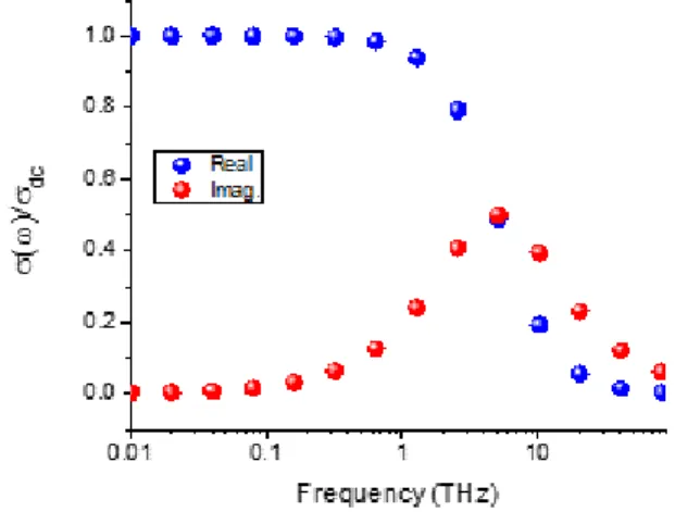
For long wavelength where the excitation energy is much smaller than the Fermi energy, graphene operates as a tunable Drude metal The optical conductivity can be described as 𝜎(𝜔) = 𝜎𝑑𝑐/(1 − 𝑖𝜔𝜏) where σDC is the DC conductivity of
graphene, ω is the angular frequency and τ scattering time of the electron. Figure 1 shows the calculated optical conductivity of graphene as a function of frequency in THz range. In sub-THz region, the optical conductivity is defined by the electrical conductance of the graphene layer. Gating the graphene layer alters the conductance and leads a significant change in the
reflection and transmission of electromagnetic waves in a very broad spectrum.
Based on this principle, Sensale-Rodriguez et al. reported graphene-based THz modulator using a back-gated transistor structure. In their device, THz-transparent Si substrate operates as a back-gate electrode[1]. Using graphene-dielectric-Si capacitor structure, the conductivity of graphene was modified by applying voltage between the Si back-gate and graphene. They further demonstrated individual and arrays of reflection and transmission type THz modulators using back-gated device geometry [2-4]. The dynamic range of the back-gated device structure is limited by the electrical breakdown of the gate-dielectric. Another approach is based on tuning the plasmon oscillations on structured graphene [5-7]. The frequency of plasmon oscillations on graphene ribbons can be tuned by the ribbon width and the charge density. Integrating graphene with metamaterials can yield another design parameter to improve the modulation depth; however it narrows the spectral window. It has been predicted that, graphene based modulators can create a modulation depth of >90% [8].
To overcome the limitation of back gated graphene devices, graphene supercapacitors were implemented as a broadband
Figure 1. Frequency dependent optical conductivity of graphene in THz frequencies calculated using scattering time of 200 fs.
THz modulator[9, 10]. In this device structure, an electrolyte is sandwiched between two graphene layers. Since graphene layers are gating each other, there is no need for a metallic gate electrode which introduce large insertion losses.
Figure 2 shows the schematic representation of the THz spatial light modulator formed by arrays of graphene supercapacitor. For this multipixel device, the THz transmittance is controlled by tuning the local charge density on the array. THz modulators is fabricated the using CVD grown large area graphene layers. We used chemical vapor deposition system to synthesize the large area (5x5 cm2)
graphene samples on ultra-smooth copper foil substrates (Mitsui Mining and Smelting Company, Ltd., B1-SBS, 100 nm surface roughness). The oxide layer on the foils was removed by hydrogen flow during the annealing step. Graphene was synthesized at 1035° C using 40 sccm CH4 and 80 sccm H2
gases. After 20 min of growth time, the samples were cooled down to the room temperature with the natural cooling rate of the furnace (20° C/min.). After the growth we laminated a polymer layer on graphene grown copper foils using hot lamination method and etched the copper foils in FeCl3 solution. After the etching process, large area graphene layers remains on polymer support. We pattered the graphene layers into 7mm wide ribbons and fabricated the SLM.
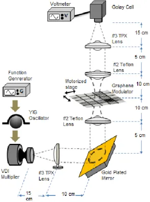
A schematic of the experimental set-up used for THz transmission measurements is given in Figure 3. A Virginia Diode, Inc. Schottky diode (VDI), based, multiplied mm-wave/THz emitter is used as a tunable frequency signal source (WR9.0AMC+WR2.8X3). Driven by a voltage-controlled frequency-tunable YIG oscillator, the system can provide a minimum average output power of about 1 mW. The source can operate in two frequency regions: 80-125 GHz and 240-380GHz. The output of the source is amplitude modulated via function generator in order to detect the radiation with a Golay Cell (Tydex TC-1T). The output beam was collimated with an F#3, D=50mm TPX lens and then focused onto the device with
an F#2, D=50mm Teflon lens. The mm-wave/THz spot diameter was measured to be ~9mm/3mm respectively at the device position. The radiation was then collected by a duplicate set of optics and focused onto the receiver. The modulator was positioned in a computer controlled XY-scanner (Marzhauser Wetzlar GmbH) which allowed the device to be raster scanned around the focused THz beam.
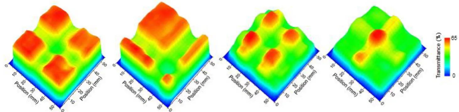
Figure 4 shows the measured transmittance map of the device at 0.37 THz. To pattern the transmittance, we apply three different voltages of -1, 0 and 1 V to the rows and columns as shown in the Figure 2c. We obtained a transmittance image (a checkerboard pattern) with maximum and minimum transmittance of 52 % and 30 %, respectively. By varying the voltage from 0 to 2 V, we can tune the transmittance from 65 % down to 30% (Figure 4b). Due to the unintentional doping of graphene and hysteresis effects, there is around 5% variation in the transmittance over the device area of 25 cm2. First we measured the transmittance image when all electrodes are grounded (Figure 2a). For this configuration, the average transmittance is around 62±5 %. The variation (±5 % of the incidence power) of the transmittance over the device area is due to inhomogeneous charge density due to unintentional doping on graphene. When we applied +1 and -1 V to the rows and columns, respectively, we observed a minimum transmittance of 30±5 %.
Figure 5 shows the recorded transmission images of the THz SLM with various voltage configuration at a frequency of
Figure 2. Schematic representation of THz spatial light modulator using graphene as an active layer.
Figure 3. Experimental setup used for the THz measurement.
0.37THz. We were able to reconfigure the transmittance through the device using a switch box that controls the voltage applied on the rows and columns. The response time of the SLM is limited by the RC time constant of the SLM which is defined by the resistance of the graphene electrodes and total capacitance of the device.
II. CONCLUSION
As a conclusion, we demonstrate a THz spatial light modulator using arrays of graphene supercapacitor. We used passive matrix addressing to control the local charge density o graphene arrays in the order of 1014 cm-2. We were able to
control local THz transmittance 65% and pattern through the 5x5 array device with a voltage bias of 2V.
III. REFERENCES
[1] B. Sensale-Rodriguez, R. Yan, M. M. Kelly, T. Fang, K. Tahy, W. S. Hwang, D. Jena, L. Liu, and H. G. Xing, "Broadband graphene terahertz modulators
enabled by intraband transitions," Nat Commun, vol. 3, pp. 780-786, Apr 2012.
[2] J. S. Gomez-Diaz, C. Moldovan, S. Capdevilla, J. Romeu, L. S. Bernard, A. Magrez, A. M. Ionescu, and J. Perruisseau-Carrier. , "Self-biased Reconfigurable Graphene Stacks for Terahertz Plasmonics.," arXiv
preprint arXiv, vol. 1405.3320, 2014.
[3] B. Sensale-Rodriguez, R. S. Yan, S. Rafique, M. D. Zhu, W. Li, X. L. Liang, D. Gundlach, V. Protasenko, M. M. Kelly, D. Jena, L. Liu, and H. G. Xing, "Extraordinary Control of Terahertz Beam Reflectance in Graphene Electro-absorption Modulators," Nano Letters, vol. 12, pp. 4518-4522, Sep 2012.
[4] B. Sensale-Rodriguez, S. Rafique, R. S. Yan, M. D. Zhu, V. Protasenko, D. Jena, L. Liu, and H. G. Xing, "Terahertz imaging employing graphene modulator arrays," Optics Express, vol. 21, pp. 2324-2330, Jan 28 2013.
[5] L. Ju, B. S. Geng, J. Horng, C. Girit, M. Martin, Z. Hao, H. A. Bechtel, X. G. Liang, A. Zettl, Y. R. Shen, and F. Wang, "Graphene plasmonics for tunable terahertz metamaterials," Nature Nanotechnology, vol. 6, pp. 630-634, Oct 2011.
[6] M. Jablan, H. Buljan, and M. Soljacic, "Plasmonics in graphene at infrared frequencies," Physical Review B, vol. 80, p. 245435, 2009.
[7] H. Min and A. H. MacDonald, "Origin of Universal Optical Conductivity and Optical Stacking Sequence Identification in Multilayer Graphene," Physical
Review Letters, vol. 103, Aug 7 2009.
[8] B. Sensale-Rodriguez, T. Fang, R. S. Yan, M. M. Kelly, D. Jena, L. Liu, and H. L. Xing, "Unique prospects for graphene-based terahertz modulators,"
Applied Physics Letters, vol. 99, Sep 12 2011.
[9] N. Kakenov, O. Balci, E. O. Polat, H. Altan, and C. Kocabas, "Broadband terahertz modulators using self-gated graphene capacitors," Journal of the Optical
Society of America B-Optical Physics, vol. 32, pp.
1861-1866, Sep 1 2015.
Figure 4. a, THz transmittance map of the device recorded at 0.37 THz. The voltage configuration of rows and column are arranged to generate chessboard pattern. B, The variation of transmittance as a function of voltage difference between the
row and column.
Figure 5. THz transmittance map of the device with different voltage configurations.
[10] N. Kakenov, T. Takan, V. A. Ozkan, O. Balci, E. O. Polat, H. Altan, and C. Kocabas, "Graphene-enabled electrically controlled terahertz spatial light modulators," Optics Letters, vol. 40, pp. 1984-1987, May 1 2015.