PAPER
Capacitance–conductance characteristics of
Au/Ti/Al
2
O
3
/n-GaAs structures with very thin Al
2
O
3
interfacial layer
To cite this article: A Turut et al 2015 Mater. Res. Express 2 046301
View the article online for updates and enhancements.
Related content
Influence of Al2O3 barrier on the interfacial electronic structure of Au/Ti/n-GaAs structures
Abdulkerim Karabulut, Hasan Efeoglu and Abdulmecit Turut
-Electrical characteristics of Au/Ti/n-GaAs contacts over a wide measurement temperature range
Necmi Biyikli, Abdulkerim Karabulut, Hasan Efeolu et al.
-Au/n-InP Schottky diodes using an Al2O3 interfacial layer grown by atomic layer deposition
Hogyoung Kim, Min Soo Kim, Seung Yu Yoon et al.
-Recent citations
Investigation of temperature dependent negative capacitance in the forward bias C-V characteristics of (Au/Ti)/Al2O3/n-GaAs Schottky barrier diodes (SBDs) Ç.. Güçlü et al
-Photodiode based on Pb0.9Cd0.1S ternary alloy semiconductor for solar tracking systems
S. Wageh et al
-Cadmium Oxide:Titanium Dioxide Composite Based Photosensitive Diode Abdulkerim Karabulut et al
-Mater. Res. Express 2 (2015) 046301 doi:10.1088/2053-1591/2/4/046301
PAPER
Capacitance–conductance characteristics of Au/Ti/Al
2
O
3
/n-GaAs
structures with very thin Al
2
O
3
interfacial layer
A Turut1,6
, A Karabulut2
, K Ejderha3
and N Bıyıklı4,5
1 Istanbul Medeniyet University, Faculty of Sciences, Engineering Physics Department, TR-34730 Istanbul, Turkey 2 Sinop University, Faculty of Engineering, Department of Electrical and Electronics Engineering, Sinop, Turkey 3 Bingöl University, Faculty of Sciences and Arts, Department of Physics, 12000 Bingöl, Turkey
4 Institute of Materials Science and Nanotechnology, Bilkent University, Bilkent, Ankara 06800, Turkey 5 National Nanotechnology Research Center (UNAM), Bilkent University, Bilkent, Ankara 06800, Turkey 6 Author to whom any correspondence should be addressed.
E-mail:[email protected],[email protected],[email protected],[email protected]
Keywords: high dielectric material, atomic layer dedeposition, MIS devices
Abstract
High-k Al
2O
3with metallic oxide thickness of about 3 nm on n-type GaAs substrate has been
deposited by the atomic layer deposition (ALD) technique. Thus, it has been formed the Au-Ti/Al
2O
3/
n-GaAs MIS structures. It has been seen that the MIS structure exhibits excellent capacitance-voltage
(C–V) and current-voltage (I–V) properties at 300 K. The saturation current of the forward bias and
reverse bias I–V characteristics was the same value. An ideality factor value of 1.10 has been obtained
from the forward bias I–V characteristics. The C–V characteristics of the structure have shown almost
no hysteresis from +3 V to
−10 V with frequency as a parameter. The reverse bias C–V curves have
exhibited a behavior without frequency dispersion and almost hysteresis at each frequency from
10 kHz to 1000 kHz.
1. Introduction
Metal/oxide (insulator)/semiconductorfield effect transistor (MOSFET) systems are important conventional devices in integrated circuit technology. MOS transistors are also increasingly used in analog applications such as switched capacitor circuits, analog-to-digital converters andfilters [1–9]. As mentioned by Wu and colleagues [10], the integrated circuit fabrication based on MOSFET relies on thermally grown amorphous SiO2as a gate
dielectric, and a stable Si:SiO2interface offers many important materials and electrical properties such as the
excellent electrical insulation and interfacial bonding properties. However, in order to avoid severe short channel effects, the gate dielectric thickness must also be reduced to the point that leakage current becomes unacceptable. Therefore, the SiO2must be replaced with other gate dielectrics [10–24], that is, the reduction of
gate dimensions requires decreasing oxide thickness to prevent the short channel effect and therefore the undesirable gate leakage current is substantial and increases exponentially with decreasing thickness. This calls for other dielectrics with much higher dielectric constants, that is, the high-κ metallic gate oxides which allow maintenance of the gate oxide capacitance needed for reducing short channel effects [10–24]. Wu and colleagues have reported [10] that the atomic layer deposition (ALD) method is the most widely used technique in spite of the fact that other methods have also led to attractive results, and that the ALD has improved the interface quality and reduced the defects density in high-κ films. Furthermore, Deposition of the SiO2onto GaAs substrate creates
a high density of interface states. These facts practically prevent implementation of MOS capacitor with GaAs substrate [1].
We have prepared the MIS (metal/insulator/semiconductor) Au/Ti/Al2O3/n-GaAs/In. The Al2O3metal
oxide layer on the GaAs substrate was formed by ALD method, and thefilm thickness of the Al2O3layer was
about 3 nm. As stated by Pan et al [12], the complementary metal oxide semiconductor (MOS) devices require gate oxide of about 1 nm to reduce the gate leakage current and maintain the gate capacitance. This is the reason RECEIVED
20 November 2014 REVISED 10 February 2015 ACCEPTED FOR PUBLICATION 25 February 2015 PUBLISHED 20 March 2015
why we take such a thickness. Thickness of conventional SiO2less than 20 Å is inevitable to excessive leakage
current due to the occurrence of direct tunneling. Therefore, silicon dioxide has to be substituted by a high dielectric constant material, which provides a physically thickerfilm for the same electrically equivalent oxide thickness [12]. Au(50 nm)/Ti(10 nm) Schottky contacts have been fabricated on Al2O3/n-GaAs structure using
magnetron dc sputter technique. Au thinfilms are more often used as a top layer to protect other metallic layers. Al2O3is an attractive candidate for the high-κ material; it has a dielectric constant of 8.6 and a wide bandgap of
about 6.6 eV (for the amorphous oxide typical of ALD-grown layers). Titanium is commonly used as a standard gate metal in the fabrication of GaAsfield effect transistors (FET) and MESFET since it has good adhesion and is stable against inter-diffusion and compound formation and has good electrical properties at room temperature and elevated temperatures [23,24].
Moreover, the method used to form the oxide layer in the MOS systems affects device performance and stability and plays an important role in integrated circuits. Furthermore, It has been examined that high-κ metallic gate oxides such as Al2O3, Nd2O3, Gd2O3and HfO2become the potential materials and high dielectric
permittivity to replace silicon dioxide SiO2[9–12], and ALD technique can be preferred to the other techniques
for the deposition of metallic gate oxide Al2O3, Nd2O3and Gd2O3due to its unparalleled uniformity and precise
thickness control technique. Pan et al [12] have reported that TiN/Nd2O3/p-Si/Al MOS capacitors withfilm
thickness of about 6.5 nm grown by reactive rf sputtering exhibit excellent electrical properties such as high electric breakdownfield and being without frequency dispersion and almost hysteresis in capacitance–voltage (C–V) curves after annealing at 700 °C treatment. Raeissi et al [13] have investigated electron capture for insulator/silicon interface states for high-κ dielectrics of Gd2O3grown on silicon wafers by molecular beam
epitaxy (MBE) and ALD, and for HfO2prepared by reactive sputtering by measuring the frequency dependence
of MOS capacitance. Kundu et al [14] have fabricated GaAs-based MOS devices with TiO2layer having three
different thicknesses of 33, 54 and 71 nm of TiO2by the sol–gel technique and they have shown that the C–V
characteristics have strongly depended on applied voltage and the interfacial layer thickness and frequency in the frequency range 10 kHz–1 MHz [14].
Long et al [16,17] reported the C–V measurements of Pd/Al2O3/GaN MOS capacitors with the Al2O3layer
of approximately 8 nm by ALD, over a temperature range of 77–500 K. They [16,17] have estimated the
interface state density of the wide band gap GaN semiconductor by the limitations of the conductance method in this temperature range, and have described the role of the pyroelectric effect in the interpretation of higher temperature capacitance–voltage data, because GaN-based devices are intended for high temperature
applications. Saghrouni et al [20,21] have described the effect of post-deposition annealing on the physical and electrical characteristics of Co/Au/Dy2O3/p-GaAs device with Dy2O3thickness of 10 nm by electron beam
deposition (EBD) under ultra-vacuum. They [20] have found that the annealed device exhibited excellent electrical properties such as small density of interface state and low leakage current, and have studied the ac impedance properties of the structures in a wide frequency range at different bias voltage, and have attributed this phenomenon to a rather crystallized Dy2O3structure and to the reduction of the defects at the oxide/GaAs
interface.
It has been stated in the above studies that metal oxides are readily formed by atomic layer deposition. The ALD process for HfO2using tetraethylmethylamido hafnium as the metal precursor has resulted in an interfacial
layer between the oxide and the semiconductor, in contrast to Al2O3deposition by ALD on surfaces such as
GaAs and InGaAs. The initial stages of the Al2O3deposition process by ALD have often been reported to result in
the decomposition of native oxides formed on the semiconductor surface, with trimethylaluminium (TMA) as the metal source [17]. Furthermore, Dy2O3, like most rare earth oxides, is not usually stoichiometric and often
contains significant concentrations of oxygen vacancies which can contribute to leakage current. Thus, it is important to evidence the effects of the native oxide and the different defects such as oxygen vacancies and grain boundaries on the electrical and dielectrical properties of MIS or MOS structures [20, 21]. The opto-electrical characteristics of MIS structures are controlled mainly by its interface properties [1–7, 25–30]. As is well-known, the C–V plot or admittance value differs significantly from that expected for an ideal MIS diode, and thus the performance of the metal oxide/GaAs-based electronic and optical devices is reduced [1–7,25–30]. Therefore, studies on interface properties are essential in the understanding of the electrical properties of the MIS structures, and are especially of technological importance for developing GaAs-based devices [25–30].
2. Experimental details
Au/Ti/Al2O3/n-GaAs MIS structures were fabricated using n-type single crystals GaAs wafer with (100) surface
orientation, having thickness of 300μm, 6.8 × 1015cm−3carrier concentration (ND) and 1.2Ω cm resistivity
(given by the manufacturer). Before the SBDs fabrication process, the experimental procedure was carried out first as a cleaning procedure, that is: sonicated for two minutes in acetone and two minutes in prophanol,
respectively; then, rinsed in DI water of resistivity of 18 MΩ cm for an extended time and dried under N2flow.
After surface cleaning of n-GaAs, high purity (99.999%), In with a thickness of about 2000Ǻ was coated for ohmic contact at a base pressure about 10−6Torr. Low ohmic contact to n-GaAs was obtained by annealing at 385 °C for three minutes under dry nitrogenflow. The ALD of Al2O3thinfilms was carried out in Cambridge
Nanotech Savannah 100 reactor. The Al2O3deposition was performed at 200 °C using trimethylaluminum
(TMA) (Al precursor), and water (oxygen precursor), for a total of 30 cycles. Standard photolithography technique was used for pattern fabrication on GaAs. An Al2O3interface layer is formed by ALD method and Au
(90 nm)/Ti(10 nm) Schottky contacts are made using magnetron dc sputter technique. Finally the photoresist was removed by washing with DI water and then with N2. The I(V) and C(V,f)− G(V,f) characteristics of the
device were measured using a Keithley 487 picoammeter/voltage source and an HP 4192 A LF impedance analyzer, respectively, at room temperature in dark.
3. Results and discussion
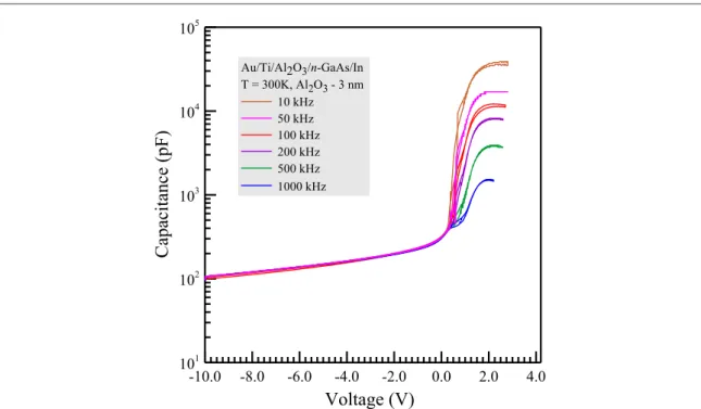
Figure1shows the experimental forward and reverse bias C–V characteristics for the MIS Au/Ti/Al2O3/n-GaAs
structure at different frequencies and 300 K. As mentioned above, the thickness of the interfacial layer Al2O3was
about 3 nm. For an MIS diode with n-type semiconductor, the curve has an accumulation region of electrons and therefore a high differential capacitance of semiconductor in series with the capacitance of the insulator at positive voltage at the right side. As a result, the total capacitance at the accumulation region is close to the capacitance of the insulator [25–30]. As the positive voltage is reduced sufficiently, a depletion capacitance
forms near the semiconductor surface, and the total capacitance decreases because the depletion region acts as a dielectric in series with the interfacial insulator layer [25–30]. As can be seen fromfigure1, the hysteresis behavior with a very narrow window was observed for the MIS C–V curves at all frequencies. It can be said that the sample has a negligibly thin interfacial-layer thickness. Another possible reason for this behavior is mobile charges in the oxide layer. This relatively smaller hysteresis phenomenon can be ascribed to the trapped charges at defect sites to be passivized due to the Al2O3layer, and to the reduction of interface traps at Al2O3layer and
GaAs interface [3,25–30].
The characterıstics parameters of the ideal Schottky diodes can be calculated using the thermionic emission (TE) current expression. The I–V equation by the forward bias TE theory is given as follows [28–31]
Figure 1. Experimental forward and reverse bias C–V characteristics for the MOS (metal/oxide layer/semiconductor) Au/Ti/Al2O3
/n-GaAs structure at different frequencies and 300 K.
3
= − −
(
)
I I q V IR nkT exp 1 , (1) 0 s ⎡ ⎣ ⎢ ⎢ ⎛ ⎝ ⎜ ⎜ ⎞ ⎠ ⎟ ⎟ ⎤ ⎦ ⎥ ⎥ Where I0is the saturation currentΦ = ⁎ − I AA T q kT exp b , (2) 0 2 ⎜ 0⎟ ⎛ ⎝ ⎞ ⎠
is the saturation current density,Φb0and n are the effective barrier height (BH) at zero bias and ideality factor
calculated from the intercept and slope of the linear portion of the semi-log forward bias ln I–V characteristics, respectively, A* is the effective Richardson constant of 8.16 A (cm2K2)−1for n-type GaAs, A is the diode area. Rs
is the series resistance of the neutral region of the semiconductor substrate between the depletion region and ohmic contact. IRsand (V–IRs) are the voltage drop across the series resistance and the depletion region,
respectively. The series resistance value of the Au/Ti/Al2O3/n-GaAs MIS diode was calculated as 11.30Ω from
the data of downward curvature region of the forward bias I–V characteristics using Cheung’s functions [31]. For values of q(V–IR) greater than 3 kT, the ideality factor is given by
ℓ = n q kT V nI d d( ). (3)
The value of n indicates the deviation from ideal forward bias characteristics for Schottky diodes. The high values of n can be attributed to effects of the bias voltage drop across the interfacial layer and, therefore, of the bias voltage dependence of the barrier height [32–46].
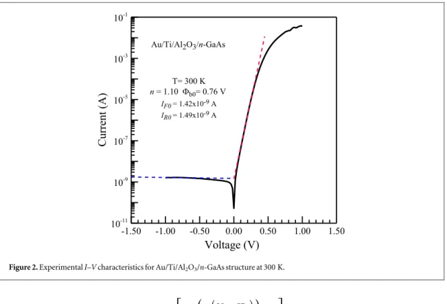
Figure2shows the semi-log reverse and forward I–V curves of the Au/Ti/Al2O3/n-GaAs MIS diode at 300 K.
The experimental values of the BH and ideality factor from the intercept and slope of the linear portion of the forward-bias lnI versus V plot have been calculated as 1.10 and 0.76 eV for 300 K, respectively. The intercepts or the saturation currents at V = 0 volts for the reverse bias and forward bias branch correspond to 1.49 × 10⁻⁹A and 1.42 × 10⁻⁹A. These values say that the device shows an excellent rectification or diode behavior. The saturation current values give a value of about 0.76 eV using equation (2). The ideality factor value of 1.10 says that the currentflow across the device is dominated by the thermionic emission over the BH because the Al2O3
interfacial layer is very thin. As mentioned by Zussman [33], the sputter process relative to the evaporation process can improve the properties of diode due to a process of cleaninig of the surface of the substrate taking place during the sputter deposition as a result of the chemical reactivity of the plasma tail and high energy of the sputtered atoms.
Goksu et al [34] used the GaAs semiconductor substrate with the same carrier concentration
(7.43 × 1015cm−3) and fabricated for Ti/n-GaAs diodes without the interfacial layer prepared by magnetron dc sputtering and obtained a BH value of 0.90 eV with an ideality factor 1.02 for this diode at 300 K. Myburg et al
[35] have fabricated Ti/n-GaAs Schottky diodes using n-GaAs epilayer layer with a free carrier concentration (Si doped) of 1 × 1016cm−3grown on n+-GaAs semiconductor substrate by organometallic vapor phase epitaxy, and they [35] have reported a BH value of about 0.83 eV with an ideality factor of 1.03 for this diode at 300 K. Dio et al [36] have measured forward and reverse bias I–V characteristics of Au/Ti/n-GaAs diodes prepared by ion
beam sputtering at different sputtering voltages and currents and they [36] have reported BH values from 0.79 to 0.83 eV and ideality factor from 1.03 to1.10 for these diodes at 300 K. Ayyildiz and Turut [37] have given a BH value of about 0.64 eV with an ideality factor of 1.08 from forward bias I–V characteristics (300 K) of Ti/n-GaAs diodes prepared by evaporation of Ti. Cola et al [38] have reported BH values from 0.828 to 0.854 eV and ideality factor values from 1.01 to1.08 (300 K) from forward bias I–V characteristics of Au/Ti/n-GaAs diodes prepared by ion beam sputtering at different sputtering voltages and currents. As can be seen, the value of 0.76 eV we have found for the Au/Ti/Al2O3/n-GaAs MIS diode prepared by magnetron dc sputtering differs from the results in
the literature given above. The reason for difference can be due to the presence of the Al2O3layer at the Au/Ti
and n-GaAs interface. Therefore, it can be said that the Al2O3layer can be used to realize the barrier height
modification in the Schottky diodes.
Let us now consider the MIS structure with the interfacial layer for the I–V characteristics. Kundu et al [14] have found ideality factor values of 1.10, 1.13 and 1.15 for n-GaN based MOS structures with TiO2thicknesses of
33, 54 and 71 nm prepared by the sol–gel technique, respectively, for which their MOS structures [14] have given the non-saturated reverse bias I–V curves. Reddy et al [22] have reported that the BH values of the Au/ BaTiO3/
n-GaN structure with values of 0.87 eV (I–V) and 1.02 eV (C–V) increases compared with those of the Au/n-GaN MS structure with 0.73 eV (I–V) and 0.96 eV (C–V). They [22] have formed BaTiO3thinfilms of about
60 nm thick on the surface of the cleaned n-GaN substrates by spin coating.
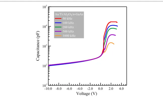
Figure3shows the experimental forward (0.0 V to 3.2 V) and reverse bias (0.0 V to−10 V) C–V characteristics for the Au/Ti/Al2O3/n-GaAs MIS structure at different frequencies and 300 K. As can be seen
fromfigure3, the capacitance curve saturates in the high forward bias voltage. These saturation regions are known as the accumulation region giving the capacitance of the interfacial layer (Al2O3) Coxand thus its
thickness. The value of Coxdetermined from the accumulation region infigure3decreases with increasing
frequency. This value is 17 000 pF at 50 kHz and 1350 pF at 1000 kHz. The values of Coxfor each frequency are
given in table1. Furthermore, the capacitance of the interfacial layer per area unit in a MIS diode is given by
ε ε
=
C A
d , (4)
ox in 0
whereε in and d are the permittivity of interfacial layer and its thickness, respectively, ε0is the permittivity of free
space and A is the area of diode. A value of 4.11 nm for the thickness of the interfacial layer Al2O3was obtained
using Coxvalue at 50 kHz in equation (4). This value is in close agreement with the Al2O3layer thickness of
n
Figure 3. Experimental forward and reverse bias C–V characteristics for the Au/Ti/Al2O3/n-GaAs structure at different frequencies
and 300 K.
5
3.0 nm formed on the GaAs wafer by ALD method. As mentioned above, the decrease in the capacitance value with increasing frequency at a given bias voltage in the plots can be attributed to the decrease of the dielectric constant value of the interfacial layer Al2O3with increasing frequency. However, this is attributed to the fact that
the interface state charges cannot follow the ac signal at sufficiently high frequencies, or increase in the capacitance with decreasing frequency is ascribed to the contribution of the interface charges in the interface states [25–30,40–62]. The decrease in capacitance value can be also due to the series resistance of the Al2O3layer
plus the neutral region of the semiconductor substrate. The series resistance of the neutral region of the semiconductor substrate between the depletion region and the back contact is the real part of the impedance. A thicker interfacial layer may cause larger series resistance. The series resistance value at each frequency can be large enough to affect the device capacitance. It can cause a serious error in the extraction of the interfacial properties, that is, the series resistance completely masks interface trap loss, and especially the equivalent parallel conductance is much more sensitive to the series resistance than capacitance. Thus, it can be said that the correction for the series resistance is particularly important in conductance measurements. Furthermore, the values of dielectric loss tangent and ac conductivity strongly depend on applied voltage and the thickness of the interfacial oxide layer [1–3,14–23].
Moreover, the low value of dielectric constant could be due to the formation of the native oxides related to Ga and As during devices fabrication processes. In addition, the diffusion of Ga and As atoms into the high-κ can exacerbate the interface quality between the high-κ dielectric and GaAs [9,12,20–22]. The dielectric constant expression of the interfacial layer is given by
ε ε = C d = A C C , (5) in ox 0 ox 0
where C0is capacitance of an empty capacitor, d is the thickness of interfacial layer Al2O3. The dielectric constant
value of the Al2O3layer was obtained using the Coxvalue from the accumulation region at each frequency in
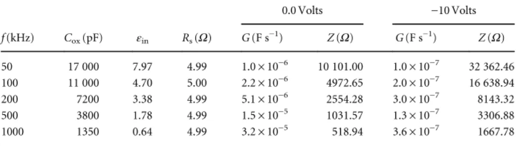
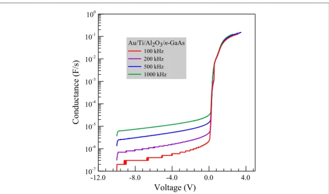
equation (5). The dielectric constant decreases with increase in frequency, as can be seen in table1. Again, as can be seen fromfigure3, the capacitance of the device is independent of the measurement frequency under the reverse bias (0.0 V to−10 V), that is, there is almost no frequency dispersion in the reverse bias. Figure4shows the phase angle versus bias voltage curves for the device at different frequencies at the room temperature. The phase angle is always 90° from−10 V to 0.0 V in the reverse bias branch, and it suddenly decreases at 0.0 V and then approaches 0° from 0.0 V to 4.0 V in the forward branch. The case clearly indicates that the diode behaves more capacitively at the reverse bias region rather than the forward bias region [51]. Figure5shows the impedance modulus (Z) versus bias voltage curves for the device at different frequencies at room temperature. It has been observed that the impedance modulus depends on frequency and bias at the reverse bias while it is frequency-independent and strongly bias-dependent for the forward bias, that is, the impedance modulus decreases with increasing frequency at a given reverse bias, and decreases with increasing bias independently of frequency by coinciding (overlap) with each other from about 0.6 V to 4.0 V at the forward bias. Figure6shows the conductance (G) versus bias voltage curves for the device at different frequencies at room temperature. The conductance is frequency-dependent and bias-dependent for the reverse bias while it is frequency-independent and strongly bias-dependent at the forward bias, that is, the conductance increases with decreasing frequency at a given reverse bias, and increases with increasing bias as independent of frequency by coinciding with each other from about 0.0 V to 4.0 V for the forward bias. The impedance modulus and conductance values at 0.0 V and−10 V are given in table1for different frequencies. It can be clearly seen from values at 0.0 V and−10 V in table1how the impedance modulus and conductance values change depending on frequency and bias voltage. This behavior indicates that the device has the same series resistance value at a given forward bias voltage for all frequencies, as can be seen in table1, thus the conductance data confirm the impedance modulus data in the forward and reverse bias regime. The series resistance expression of the MIS devices is given by [3]
Table 1. Experimental values from the reverse and forward bias characteristics for the Au/Ti/Al2O3/n-GaAs
MIS structure at different frequencies and 300 K.
0.0 Volts −10 Volts f (kHz) Cox(pF) εin Rs(Ω) G (F s−1) Z (Ω) G (F s−1) Z (Ω) 50 17 000 7.97 4.99 1.0 × 10⁻⁶ 10 101.00 1.0 × 10⁻⁷ 32 362.46 100 11 000 4.70 5.00 2.2 × 10⁻⁶ 4972.65 2.0 × 10⁻⁷ 16 638.94 200 7200 3.38 4.99 5.1 × 10⁻⁶ 2554.28 3.0 × 10⁻⁷ 8143.32 500 3800 1.78 4.99 1.5 × 10⁻⁵ 1031.57 1.3 × 10⁻⁷ 3306.88 1000 1350 0.64 4.99 3.2 × 10⁻⁵ 518.94 3.6 × 10⁻⁷ 1667.78
= + R G G w C , (6) s m m2 2 m2
where Gmand Cmare the experimental conductance and capacitance values from the strong accumulation
region for each frequency. The series resistance of the device is obtained using Gmand Cmvalues given in table1
in equation (6). As can be seen in table1, the series resistance value of the device for each frequency approximately equals 5Ω.
In C–V measurements, the charges at the interface states cannot follow the ac signal at very high frequencies [40–62], and the equivalent circuit of device will be just the interfacial layer and depletion (the space charge region) capacitance in series. At very high frequency, the total capacitance, C, per area unit of MIS diode is a
Figure 4. Experimental forward and reverse bias phase-voltage characteristics for the Au/Ti/Al2O3/n-GaAs structure at different
frequencies and 300 K.
Figure 5. Experimental forward and reverse bias impedance modulus-voltage characteristics for the Au/Ti/Al2O3/n-GaAs structure at
different frequencies and 300 K.
7
series combination of the depletion capacitance of the semiconductor CDand the capacitance of the interfacial
layer Cox, and thus the total capacitance C is represented by [27–30,45–50]
= +
C C C
1 1 1
, (7)
D ox
Coxis the capacitance of the interfacial layer and corresponds to the maximum capacitance of the MIS diode, and
CDdepends on the bias voltage. It has been stated above that the C–V curve has an accumulation region at
positive voltage at the right side which gives the capacitance of the insulator [27–30], as can be seen fromfigures1
or3. A depletion capacitance forms near the semiconductor surface from the positive voltage to negative, or as the positive voltage is reduced sufficiently, and the total capacitance decreases because the depletion region acts in series with the interfacial insulator layer [27–30]. Thus, in this case, it can be said that the negative voltage region infigures1and3corresponds to the deep depletion condition [3,27–30]; the depletion capacitance CD
can approximately be given by [27–30,46–50]
Φ ε = − −
(
)
C V V q N A 1 2 , (8) bCV D2 0 n s d 2where Vnis the potential difference between the Fermi level and the conduction band minimum in the neutral
region of n-type semiconductor, Φ( b0CV−Vn)= VD0is the diffusion potential at the zero bias, Ndis the doping
concentration of the n-type semiconductor,εsis the permittivity of the semiconductor, q is the electronic charge
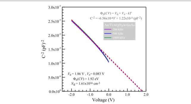
and A is the diode area. Figure7shows the experimental reverse bias C−2–V characteristics for the Au/Ti/Al2O3/
n-GaAs structure at various frequencies and 300 K. As can be seen from equation (7), the C−2versus V plot is a straight line whose intercept with V axis gives the value of V0= VD0, and the slope gives the value of Nd. Ndcan be
given as follows: ε = −
( )
N q A V C 2 d d . (9) d s 2 2The values of V0= 1.86 V, Vn= 0.083 V, Φb0CV = 1.92 Vand Nd= 1.61 × 1016cm−3were obtained from the
experimental reverse bias C−2–V plot. As can be seen from the obtained barrier height values, there is an appreciable difference between the barrier height values obtained I–V and C–V characteristics. That is, the barrier height value from I–V characteristics is much lower than that from the C–V characteristics. Likewise, the experimental carrier concentration value of Nd= 1.61 × 1016cm−3from C–V characteristics is significantly
higher than the value of 7.43 × 1015cm−3given for the n-GaAs used this study. The barrier height and carrier concentration change in the MS contacts with the interfacial layer depends on the position of the Fermi level and interface-state density. The change in positive or negative interface charge will affect the depletion layer of the
Figure 6. Experimental forward and reverse bias conductance-voltage characteristics for the Au/Ti/Al2O3/n-GaAs structure at
semiconductor, and therefore the Fermi-level position. In the absence of the interface states, the negative charge on the metal surface must be equal to the positive space charge due to the neutrality condition. The increase in the barrier height and carrier concentration is evidence for the presence of the negative interface charge, and thus for the positive space charge increase due to the neutrality condition [30,55,56].
4. Conclusion
It has been seen that the MIS structure with a high-κ the Al2O3gate dielectric that we have grown by the ALD on
the n-GaAs substrate exhibits excellent electrical properties, that is, the structure has shown almost no hysteresis over the whole bias region and no frequency dispersion in the reverse bias C–V curves for all frequencies. This film appears to be a very promising high-κ gate dielectric with very thin film of about 3 nm for future ultra-large scale integration devices.
Acknowledgments
This work was performed in part at the UNAM-Institute of Materials Science and Nanotechnology which is supported by the State Planning Organization of Turkey through the National Nanotechnology Research Center Project. The measurements were made at Department of Physics, Faculty of Sciences and Arts, Bingöl
University, Turkey.
References
[1] Colinge C P and Colinge C A 2002 Physics of Semiconductor Devices (Dordrecht: Kluwer) [2] Dimitrijev S 2012 Prenciples of Semiconductor Devices (Oxford: Oxford University press)
[3] Nicollian E H and Brews J R 1982 MOS (Metal Oxide Semiconductor) Physics and Technology Bell Laboratories, Murray Hill (New York: Wiley)
[4] Oh S-K, Shin H-S, Li M, Lee H, Lee G-W and Lee H-D 2014 Japan. J. Appl. Phys.53 08NE05
[5] Pakma O, Serin N, Serin T and Altındal Ş 2008 J. Appl. Phys.104 014501
[6] Caldıran Z, Deniz A R, Coskun F M, Aydogan S, Yesildag A and Ekinci D 2014 J. Alloys Compd.584 652–7
[7] Ozdemir A F, Aydin S G, Aldemir D A and Gursoy S S 2011 Synth. Met.161 692–7
[8] Kaya A, Zeyrek S, San S E and Altındal Ş 2014 Chin. Phys. B23 018506
[9] Mönch W 2005 Appl. Phys. Lett.86 122101
[10] Wu M, Alivov Y I and Morkoc H 2008 J. Mater. Sci., Mater. Electron.19 915–51
[11] Ye P D et al 2003 IEEE Electron Device Lett.24 209
[12] Pan T-M, Lee J-D, Shu W-H and Chen T-T 2006 Appl. Phys. Lett.89 232908
[13] Raeissi B, Piscator J, Engström O, Hall S, Buiu O, Lemme M C, Gottlob H D B, Hurley P K, Cherkaoui K and Osten H J 2008 Solid-State Electron.52 1274–9
[14] Kundu S, Roy S K and Banerji P 2011 J. Phys. D: Appl. Phys.44 155104
[15] Kınacı B, Cetin S S, Bengi A and Ozcelik S 2012 Mater. Sci. Semicond. Process.15 531–5
Figure 7. Experimental reverse bias C−2–V characteristics for the Au/Ti/Al2O3/n-GaAs structure at different frequencies and 300 K.
9
[16] Long R D, Hazeghi A, Gunji M, Nishi Y and McIntyre P C 2012 Appl. Phys. Lett.101 241606
[17] Long R D and McIntyre P C 2012 Materials5 1297–335
[18] Bioki H A 2013 Eur. Phys. J. Appl. Phys.62 20201
[19] Gupta R K and Yakuphanoglu F 2013 Microelectron. Eng.105 13–7
[20] Saghrouni H, Jomni S, Belgacem W, Hamdaoui N and Beji L 2014 Physica B444 58–64
[21] Saghrouni H, Jomni S, Belgacem W, Elghoul N and Beji L 2015 Mater. Sci. Semicond. Process.29 307–14
[22] Reddy V R, Manjunath V, Janardhanam V, Kil Y-H and Choi C-J 2014 J. Electron. Mater.43 3499
[23] Cherif A, Jomni S, Belgacem W, Elghoul N, Khirouni K and Beji L 2015 Mater. Sci. Semicond. Process.29 143–9
[24] Aksoy S and Caglar Y 2014 J. Alloys Compd.613 330–7
[25] Mir F A, Rehman S, Mir T A, Asokan K and Khan S H 2014 Appl. Phys. A116 1017–23
[26] Selcuk A B, Ocak S B, Aras F G and Orhan E O 2014 J. Electron. Mater.43 3263–9
[27] Saglam M, Türüt A, Nuhoglu Ç, Efeoglu H, Kılıçoglu T and Ebeoglu M A 1997 Appl. Phys. A65 33–7
[28] Sze S M 1981 Physics of Semiconductor Devices 2nd edn (New York: Wiley) [29] Neamen D A 1992 Semiconductor Physics and Devices (Boston: Irwin)
[30] Rhoderick E H and Williams R H 1988 Metal-Semiconductor Contacts 2nd edn (Oxford: Clarendon) [31] Cheung S K and Cheung N W 1986 Appl. Phys. Lett.49 85
[32] Karataş Ş, Altındal Ş and Çakar M 2005 Physica B357 386–97
[33] Zussman A 1986 J. Appl. Phys.59 3894–900
[34] Goksu T, Yıldırım N, Korkut H, Ozdemir A F, Turut A and Kokce A 2010 Microelectron. Eng.87 1781–4
[35] Myburg G, Auret F D, Meyer W E, Louw C W and van Staden M J 1998 Thin Solid Films325 181–6
[36] Dio M D, Cola A, Lupo M G and Vasanelli L 1995 Solid-State Electron.38 1923–8
[37] Ayyildiz E and Turut A 1999 Solid-State Electron.43 521–7
[38] Cola A, Lupo M G, Vasanelli L and Valentini A 1992 J. Appl. Phys.71 4966–70
[39] Mönch W 2008 Appl. Phys. Lett.93 172118
[40] Turut A, Sağlam M, Efeoğlu H, Yalcin N, Yildirim M and Abay B 1995 Physica B205 41–50
[41] Bestas A N, Yazıcı S, Aktas F and Abay B 2014 Appl. Surf. Sci.318 280–4
[42] Guzeldir B, Sağlam M, Ates A and Turut A 2015 J. Alloys Compd.627 200–5
[43] Doğan H and Elagöz S 2014 Physica E63 186–92
[44] Tombak A, Ocak Y S, Genişel M F and Kilicoglu T 2014 Mater. Sci. Semicond. Process28 98–102
[45] Doğan H, Yıldırım N, Orak İ, Elagöz S and Turut A 2015 Physica B457 48–53
[46] Rhoderick E H 1970 J. Phys. D: Appl. Phys.3 1153
[47] Chattopadhyay P and Raychaudhri B 1993 Solid-State Electron.36 605–10
[48] Ateş A, Güzeldir B and Sağlam M 2011 Mater. Sci. Semicond. Process.14 28–36
[49] Fonash S J 1983 J. Appl. Phys.54 1966
[50] Aydogan S, Saglam M and Turut A 2012 Microelectron. Reliab.52 1362–6
[51] Kim C H, Yaghmazadeh O, Tondelier D, Jeong Y B, Bonnassieux Y and Horowitz G 2011 J. Appl. Phys.109 083710
[52] Korucu D, Duman S and Turut A 2015 Mater. Sci. Semicond. Process.30 393–9
[53] Sellai A, Mamor M and Al-Harthi S 2007 Surf. Rev. Lett.14 765–8
[54] Tuğluoğlu N, Yüksel Ö F, Karadeniz S and Şafak H 2013 Mater. Sci. Semicond. Process.16 786–91
[55] Biber M and Turut A 2002 J. Electron. Mater.31 1362
[56] Mönch W 1995 Semiconductor Surfaces and Interfaces 2nd edn (Berlin: Springer) pp 75–84 364 and 382–387 [57] Gullu O, Cankaya M, Bibe M and Turut A 2008 J. Phys.: Condens. Matter20 215210
[58] Gunduz B, Yahia I S and Yakuphanoglu F 2012 Microelectron. Eng.98 41–57
[59] Ozdemir A, Gok A and Turut A 2007 Thin Slid Films515 7253–8
[60] Duman S, Ozcelik F S, Gurbulak B, Korucu D, Baris O and Turgut G 2014 Mater. Sci. Semicond. Process.28 20–5
[61] Asar Y S, Asar T, Altındal S and Ozcelik S 2015 J. Alloys Compd.628 442