PROBING HOT-ELECTRON EFFECTS IN
PLASMONIC SURFACES USING X-RAY
PHOTOELECTRON SPECTROSCOPY
A THESIS
SUBMITTED TO THE MATERIALS SCIENCE AND NANOTECHNOLOGY PROGRAM
AND THE GRADUATE SCHOOL OF ENGINEERING AND SCIENCE OF BILKENT UNIVERSITY
IN PARTIAL FULFILLMENT OF THE REQUIREMENTS FOR THE DEGREE OF
MASTER OF SCIENCE
By
Andi Çupallari
May 2014
ii
I certify that I have read this thesis and that in my opinion it is fully adequate, in scope and in quality, as a thesis for the degree of Master of Science.
. Assist. Prof. Dr. Aykutlu DÂNA (Advisor)
I certify that I have read this thesis and that in my opinion it is fully adequate, in scope and in quality, as a thesis for the degree of Master of Science.
.
Prof. Dr. Raşit TURAN
I certify that I have read this thesis and that in my opinion it is fully adequate, in scope and in quality, as a thesis for the degree of Master of Science.
.
Assist. Prof. Dr. Ali Kemal OKYAY
Approved for the Graduate School of Engineering and Science:
.
Prof. Dr. Levent Onural Director of the Graduate School
iii
ABSTRACT
PROBING HOT-ELECTRON EFFECTS IN PLASMONIC
SURFACES USING X-RAY PHOTOELECTRON SPECTROSCOPY
Andi Çupallari
M.S. in Materials Science and Nanotechnology Supervisor: Assist. Prof. Dr. Aykutlu DÂNA
May, 2014
Hot-electron effects in plasmonic structures have been recently investigated as potential alternative mechanisms for solar energy harvesting and photodetection. [1][2][3] Hot-electron effects provide a semiconductor free route for the conversion of photons into electrical power. Here we investigate plasmonic hot electron effects in Metal-Insulator-Metal (MIM) structures using X-ray photoelectron spectroscopy (XPS). XPS has been previously used to investigate optoelectronic effects in semiconductors and nanocomposite surfaces. [4][5][6] Here, a similar approach is used to characterize the plasmonic and hot electron effects in MIM Junctions. Monochromatic Laser excitation with 450, 532 and 650 nm wavelengths are employed to illuminate the plasmonic surfaces fabricated using thermal evaporation, atomic layer deposition and electron beam lithography. The top metal of the MIM structures act as the plasmonic antenna (metal nanodiscs and gratings/stripes) that provide wavelength selective or wide band optical absorption. Plasmonic enhancement at the interface between the top metal and the insulator enhances the absorption of light in the device and leads to excitation of a larger number of hot electrons from the metal. Hot electron effects are characterized through studying the metal-insulator-metal junction and comparing shifts of binding energy belonging to the top metal islands for dark and illuminated conditions. XPS spectrum provides important information regarding the plasmonic and hot electron effects in the interface between top metal and the dielectric. A
iv
systematic study of the dependence of the XPS spectra on excitation wavelength, light intensity, polarization, insulator thickness and nanostructure geometry is presented. Effects of using different metals and insulator materials are also studied in symmetric and asymmetric tunnel junctions.
Keywords: X-ray photoelectron spectroscopy, plasmonics, Metal-Insulator-Metal (MIM), plasmonic antenna, metal nanoparticles, hot-electron effects
v
ÖZET
PLAZMONİK YAPILARDA SICAK ELEKTRON ETKİLERİNİN
X-IŞINI SPEKTROSKOPİSİ METODUYLA GÖZLEMLENMESİ
Andi Çupallari
Malzeme Bilimi ve Nanoteknoloji, Yüksek Lisans Tez Yöneticisi: Yrd. Doç. Dr. Aykutlu DÂNA
Mayıs, 2014
Sıcak-elektronların plazmonik yapılarda oluşturduğu etkiler bir süredir güneş enerjisi dönüşümü ve fotodetektör teknolojisinde alternatif mekanizmalar olarak araştırılmaktadır. Potansiyel olarak, sıcak elektron etkileri fotonların elektriksel güce çevrilmesi için yarı iletken içermeyen bir yol sağlamaktadır. [1][2][3] Burada, X-ışını fotoelektron spektroskopisi (XPS) kullanarak sıcak elektronun metal-yalıtkan-metal yapılar üzerindeki etkilerini araştırmaktayız. XPS geçmiş yıllarda yarı iletken malzemelerde ve nanokompozit yüzeylerde optoelektronik etkileri araştırmak için kullanılmıştır.[4][5][6] Buna benzer bir yöntem ile, metal-yalıtkan-metal yapılardaki plazmonik ve sıcak elektron etkileri karakterize edilmektedir. Dalga boyu 450 nm, 532 nm ve 650 nm olan lazerler, termal buharlaştırıcı, atomik boyutta katman kaplama ve elektron ışını litografisi kullanılarak elde edilen plazmonik yüzeyleri aydınlatmak için kullanılmıştır. Plazmonik anten (metal nanodiskler ve ızgaralı/şeritli yapılar) olarak davranan metal-yalıtkan-metal yapıların üst tabakasındaki metal, dalgaboyu seçici ya da geniş bant optik soğurma sağlamaktadır. Üst metal tabaka ve yalıtkan ara yüzeydeki plazmonik güçlendirme yapıdaki ışığın soğrulmasını arttırmakta ve metalden daha çok sayıda sıcak elektronun uyarılmasına öncülük etmektedir. Sıcak elektron etkileri üst metal tabakanın bağlanma enerjisindeki kaymaların karanlık ve aydınlık ortamlardaki karşılaştırılması ile karakterize edilmiştir. XPS spektrumu üst metal tabaka ve yalıtkan ara yüzeydeki plazmonik ve sıcak elektron etkileri hakkında önemli
vi
bilgiler sağlamaktadır. XPS spektrumunun, plazmonik uyarılma dalga boyu, ışık yoğunluğu, polarizasyon, yalıtkan kalınlığı ve nanoyapı geometrisi ile olan ilişkisi sistematik bir şekilde sunulmuştur. Simetrik ve asimetrik tünel bariyerlerinde alttaş ve yalıtkan olarak farklı malzemeler kullanılmasının etkileri de ayrıca çalışılmıştır.
Keywords: X-ışını fotoelektron spektroskopisi, plazmonik, metal-yalıtkan-metal yapıları, metal nanoparçacıklar, sıcak elektron etkileri
vii
viii
Acknowledgement
I would like to express my profound gratitude to my advisor, Prof. Aykutlu Dâna for his guidance and support. Without his advices and ideas finishing this thesis would have been impossible.
A special thank goes to my group mate and friend Sencer Ayas for his assistance and help during all the time. He has been my guide since the very first days I started the MS degree.
I would also like to thank all the other group members and office friends. I would also thank all the technicians and engineers working at UNAM who have helped immensely during my research.
I thank UNAM and its director, Prof. Mehmet Bayındır for their support. I also thank TUBİTAK for the material support.
ix
Contents
Acknowledgements ... viii1 Introduction
... 12 Theoretical Background
... 4 2.1 Surface Plasmon ... 42.1.1 The Wave Equation ... 4
2.1.2 Surface Plasmon at a Metal Dielectrics Interface ... 7
2.1.3 Prism Coupling Scheme ... 12
2.1.4 Grating Coupling Scheme ... 14
2.2. Localized Surface Plasmons ... 15
2.2.1. Localized Surface Plasmon Modes ... 16
2.2.2. Coupling of Localized Surface Plasmons ... 19
2.3. X-ray photoelectron spectroscopy (XPS) ... 22
2.4. Metal-Insulator-Metal Junctions ... 23
2.4.1. Basics of Metal-Insulator-Metal Junctions ... 24
2.4.2. Plasmonic Effects in MIM Structures. ... 28
2.4.3. QM Tunneling Mechanisms in MIM Structures. ... 32
3
Hot-electron and Plasmonic effects in Metal- Insulator-Metal
sandwiched structures
... 344 Fabrication and Characterization of Plasmonic Surfaces
... 405 X-ray Photoelectron Spectroscopy Experiments, Results and
Discussion
... 66x
5.1. Experimental setup ... 68
5.2. Effect of the top metal Nanostructure geometry ... 70
5.3. Effect of the insulator spacer thickness ... 83
5.4. Polarization dependence ... 90
5.5. Effect of excitation wavelength ... 92
5.6. Effect of electron flood gun on the binding energy shifts. ... 96
5.7. Effect of Laser light intensity. ... 100
5.8. Gratings experiment ... 103
6 Conclusion
…...……….……… 107xi
List of Figures
Figure 2.1. Waveguide geometry used. Waves propagate in the x-direction ... 7 Figure 2. 2. SPP propagate at the metal/insulator interface ... 8 Figure 2. 3 Field decaying at the interface. Decay length depends on the propagation constant in the film. Decay length is longer in the insulator than in the metal film. ... 11 Figure 2. 4. E-field lines of Surface Plasmon Polaritons on a Metal- dielectrics interface ... 11 Figure 2. 5. Dispersion curves and photonic lines for air and silica.[17] ... 13 Figure 2. 6. Kretschmann configuration. SPP excitation occurs only at the
metal-air interface. ... 13 Figure 2. 7. The plasmonic dispersion relation for grating coupling. [17] ... 15 Figure 2. 8. A conducting sphere under the effect of an electric field E. The medium is assumed to be air having an dielectric constant εm. [Adapted from reference 7] ... 17 Figure 2. 9. Near field coupling between near neighboring metal nanoparticles. Charge polarization caused by incoming light of two different polarization cases are shown. [Adapted from 7] ... 21 Figure 2. 10. Schematic representation of the photoelectron effect ... 23
xii
Figure 2. 11. Band diagrams of ideal MIM junctions. At diagram a) same metals are used and at b) different metals are used. Equilibrium is assumed at both cases. Bent of the vacuum energy band due to applied voltage is not shown. 25 Figure 2.12. Theoretical Tunnel Resistance as a Function of Applied Voltage for an Asymmetrical MIM Structure. [11] ... 26 Figure 2. 13. Energy band diagram of MIM junctions under different bias conditions. From left to right: No bias, Reverse Bias, Forward Bias. [13] ... 28 Figure 2.14. MIM structure geometry. The coordinative system shown is used in derivations. ... 30 Figure 2.15. Dispersion plot for MIM structure [20] ... 30 Figure 2. 16. Schematic view of tunneling mechanisms. a)Direct tunneling, b)Fowler-Nordheim Tunneling, c)Trap-assisted Tunneling [14] ... 33
Figure 3.1. Photocurrent caused by electrons passing through the barrier. Photoelectrons are excited at the top and bottom metals as well, so backward current will be produced even if less than the forward current. Here a voltage has been applied.[3] ... 35 Figure 3. 3 Energy diagram of the MIM device. Electrons are excited to higher energy states (hot electrons) incoming photons with energy hγ. Hot carriers are excited in the top and bottom metal as well. [2] ... 38 Figure 3.2. Mechanism of hot electron transmission in MIM devices in cases when excitation of SPs and direct illumination. [2] ... 38
xiii
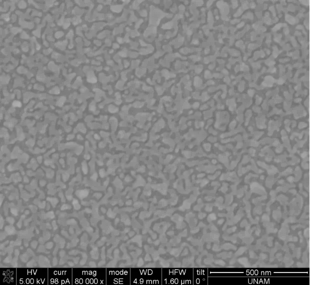
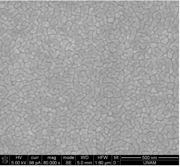
Figure 4. 1. Savanah Atomic Layer Deposition system at UNAM [25] ... 41 Figure 4. 2. SEM image, 1 nm Ag is deposited on Silicon. Random silver nanoislands of diameter 7-10 nm are formed. Nearly all the particles are independent and not connected to each other. ... 44 Figure 4. 3. SEM image, 3 nm Ag is deposited on Silicon. Diameter of the randomly formed silver nanoislands is larger that in the previous case. Here the nanoparticles have a diameter of average 20-30nm. Also the distance between neighboring islands decreases. ... 45 Figure 4. 4. SEM image, 5 nm Ag is deposited on Silicon. Here the nanoislands shown in the previous cases are connected to each other. Still it cannot be claimed to be a continuous half-film. Empty space between is still comparable in area to the to the area of the Ag structure. ... 46 Figure 4. 5. SEM image, 7 nm Ag is deposited on Silicon. Here a quasi-continuous film is formed. Empty space between Ag is obviously less than the following case. It seems that most of the Ag layer is interconnected. Also the structure has larger dimensions than the previous case where 5 nm Ag is deposited. ... 47 Figure 4. 6. SEM image, 9 nm Ag is deposited on Silicon. Here a continuous film is formed. ... 48 Figure 4. 7. Schematic representation of the fabricated device. Different samples were used having HfO2 thicknesses of 5, 10, 20 and 30 nm. Also the top Ag
metal was deposited at different quantity in order to obtain nano-islands of different dimensions. ... 50 Figure 4. 8. SEM image of the as deposited Ag (1nm) on top of HfO2 layer. The
xiv
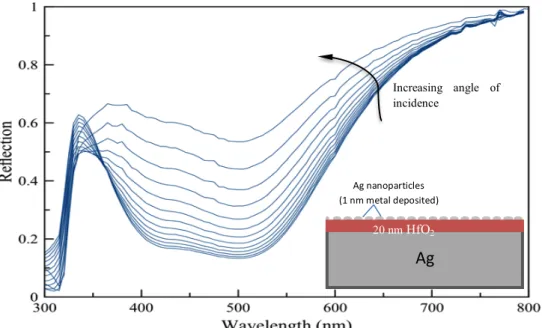
presence of the insulator. Also the bottom metal structure is visible in the background. ... 51 Figure 4. 9. Reflection spectra (p-polarization) for sample having 5 nm oxide layer in between the bottom Ag layer and the 1 nm deposited Ag top metal. Spectra is shown for angles of incidence between 15°- 75°, with 10 ° intervals. ... 52 Figure 4. 10 Figure 4.10. Reflection spectra (p-polarization) for sample having 10 nm oxide layer in between the bottom Ag layer and the 1 nm deposited Ag top metal. The spectra is shown for angles of incidence between 15°- 75°, taken with 10 ° intervals. ... 52 Figure 4.12 Reflection spectra (p-polarization) for sample having 30 nm oxide layer in between the bottom Ag layer and the 1 nm deposited Ag top metal. The spectra is shown for angles of incidence between 15°- 75°, taken with 10 ° intervals. ... 53 Figure 4. 11. Reflection spectra (p-polarization) for sample having 20 nm oxide layer in between the bottom Ag layer and the 1 nm deposited Ag top metal. The spectra is shown for angles of incidence between 15°- 75°, taken with 10 ° intervals. ... 53 Figure 4. 13. SEM image of the as deposited Ag (3nm) on top of HfO2 layer.
Dimension of the formed nanoparticles is different than the case when the same Ag quantity was deposited directly on silicon. ... 54 Figure 4. 14. Reflection spectra (p-polarization) for sample having 5 nm oxide layer in between the bottom Ag layer and the 3 nm deposited Ag top metal. The spectra is shown for angles of incidence between 15°- 75°, taken with 10 ° intervals. ... 56
xv
Figure 4. 15. Reflection spectra (p-polarization) for sample having 10 nm oxide layer in between the bottom Ag layer and the 3 nm deposited Ag top metal. The spectra is shown for angles of incidence between 15°- 75°, taken with 10 ° intervals. ... 56 Figure 4. 16. Reflection spectra for sample having 20 nm oxide layer in between the bottom Ag layer and the 3 nm deposited Ag top metal. The spectra is shown for angles of incidence between 15°- 75°, taken with 10 ° intervals. .. 57 Figure 4. 17 Reflection spectra (p-polarization) for sample having 30 nm oxide layer in between the bottom Ag layer and the 3 nm deposited Ag top metal. The spectra is shown for angles of incidence between 15°- 75°, taken with 10 ° intervals. ... 57 Figure 4. 18. SEM image of the as deposited Ag (5nm) on top of 20 nm HfO2
layer. ... 59 Figure 4. 19. Reflection spectra (p-polarization) for sample having 5 nm oxide layer in between the bottom Ag layer and the 5 nm deposited Ag top metal. The spectra is shown for angles of incidence between 15°- 75°. Most of light is reflected (~80% reflection). ... 60 Figure 4. 20. Reflection spectra (p-polarization) for sample having 10 nm oxide layer in between the bottom Ag layer and the 5 nm deposited Ag top metal. The spectra is shown for angles of incidence between 15°- 75°, taken with 10° intervals. ... 60 Figure 4. 21 Reflection spectra (p-polarization) for sample having 20 nm oxide layer in between the bottom Ag layer and the 5 nm deposited Ag top metal.
xvi
The spectra is shown for angles of incidence between 15°- 75°, taken with 10° intervals. ... 61 Figure 4. 22. Reflection spectra (p-polarization) for sample having 30 nm oxide layer in between the bottom Ag layer and the 5 nm deposited Ag top metal. The spectra is shown for angles of incidence between 15°- 75°, taken with 10° intervals. ... 61 Figure 4. 23. Fabrication of metal stripes using e-beam lithography. a) Thermal
deposition of Ag on Silicon (Ge wetting layer of 3 nm thickness not shown). b) 15 nm HfO2 is deposited by ALD. c) ~100nm PMMA is spin coated and
annealed for 90 seconds at 180˚C. d) Pattern is formed using e-beam lithography system, and then the resist is developed. e) 50nm of Ag is deposited using thermal deposition. f) Lift-off to obtain the final patterns. ... 63 Figure 4. 24 Figure 4.24. SEM image of the gratings. Width of the gratings is 150 nm and period is 250 nm, length of each strip being 50 µm. The dimensions of each set are 250µm X 250µm, and each set contains an array of 5X5 groups of gratings, and there are 200 strips in each grating. ... 64 Figure 4. 25. a) Magnetic mode; Magnetic field is confined between nanoparticle and ground plane, b) Electric mode; Magnetic Field is confined to interparticle spacing and c) magnetic and electric resonances shown in a reflection spectra. ... 66
Figure 5. 1. Experimental setup. Shown is the Laser aligned with the help of the optical setup. The LED is removed so that the Laser light can enter the chamber of the XPS. The vacuum is not affected since thick glass is placed
xvii
normally after the LED. Reflection of the Laser light from the glass is neglected. ... 69 Figure 5.2. Laser used during the experiments ... 69 Figure 5. 3. The Laser is aligned in the beginning of the experiment. Red, blue and Green Laser spots are shown. XPS data is taken only from the green circle shown in the middle. ... 70 Figure 5.4. Native binding energy spectra of Ag3d from literature a)[29] and from our experiments b) . Here the metal is grounded and electrons lost via photoelectric effect will immediately be replaced by electrons from the ground, preventing shifts in the spectra. ... 72 Figure 5.5. Shifts of the Ag 3d spectra when illuminated by Blue Laser light (λ=445nm) for top metal 1nm, 3nm and 5nm thick deposited. For 5 nm thick top metal film the binding energy is very close to native value of B.E. The reason of this is explained later. ... 73 Figure 5.6 Schematic view of the effect that x-rays have on the band diagram of the MIM structure. The surface is exposed only to x-rays a), in b) the symmetric band diagram is shown for Ag-HfO2-Ag plasmonic structure.
X-rays change the band diagram structure, and tunneling electrons from the bottom metal compensate the lost electron in the top metal nanoparticles, causing for equilibrium to be reached at about 1 eV lowering of top metal band. The bottom metal Fermi level is taken as a reference (0 eV). ... 76 Figure 5.7. Band diagram of the structure, only Laser light is shined on the surface. Hot electrons cause a current flow in both directions. Due to the symmetry of the band diagram, these currents are equal and the net current sums to zero. 76
xviii
Figure 5.8. Both x-rays and Laser light hit the surface. Shown is band diagram of Ag-HfO2-Ag MIM structure at this case b). During x-ray exposure, positive
charges accumulate in the top metal, lowering the top metal band and bending the insulator band by approximately 1 eV. ... 77 Figure 5.9. FTDT simulation results for the electric field enhancement shown for samples having 5nm insulator and 1 a), 3 b) and 5 nm c) Ag on top. ... 79 Figure 5.10. a) Spectroscopic results for the 15 degree reflection spectra
(p-polarization) of the Ag(70 nm)-HfO2(5nm)-Ag(1,3,5 nm) MIM structure
samples. Resonances shift towards higher wavelengths with increasing the nanoparticle sizes. b) FTDT simulation results. ... 81 Figure 5.11. Laser off-on process was repeated 3 times consecutively for the 1nm a), 3nm b) and 5nm Ag c) on top of 5 nm HfO2. The process is repeatable,
and the peaks continue to shift towards lower energies approaching Ag’s native Binding energy value, 368.3 eV. ... 82 Figure 5.12. Shifts of the Ag 3d spectra when sample having 70nm bottom Metal, 3nm top metal and a) 20 nm and b) 30nm insulator thickness is illuminated by Blue Laser light (λ=445nm). ... 84 Figure 5. 13. Intensity of the blue Laser light was held constant during the XPS data acquisition. XPS collects data only from the area marked with a green circle. ... 85 Figure 5. 14. Reflection results from ellipsometre measurement. The result is shown for p-polarized light, 15° angle of incidence. The sample having 30 nm insulator layer is better absorber than the one having 20 nm insulator layer. . 86
xix
Figure 5. 15. Red Laser illuminates the sample (a), exciting hot electrons up to a kinetic energy equal to the incident photon energy 1.907 eV. This is not enough to overcome the barrier. When the x-rays gun is turned on (data acquisition), the insulator band is bent (b) and the barrier becomes thinner in the bottom metal side. It is then easier for the hot electrons excited in the bottom metal to tunnel the barrier (Fowler-Nordheim tunneling). ... 88 Figure 5.16.Intensity of the red Laser light was held constant during the XPS data acquisition. XPS collects data only from the area marked with a green circle.88 Figure 5.17. Shifts of the Ag 3d spectra. Samples having 70nm bottom metal, 3nm
top metal and a) 10 nm, b) 20nm and c) 30 nm insulator thicknesses are illuminated with red Laser light (λ=650nm). The shift in spectra increases with increasing spacer thickness. The explanation given for the blue light illumination case is valid here too, with the difference that here the Fowler-Nordheim tunneling mechanism is responsible for the current, hence for the shifts in binding energies too. ... 89 Figure 5.18. Polarizer used in the experiment. ... 90 Figure 5.19. Energy shifts are polarization independent. Non-perfection intensity splitting of the polarizer is responsible for the differences in the shifts between 0° and 90° polarizer rotation cases. ... 91 Figure 5. 20.The schematic view of the sample used shown in a) and the band diagram when Laser lights of different wavelengths illuminate the sample shown in b). Note the built in potential of 0.5 V in the insulator band. ... 92 Figure 5. 21. Shifts of the Ag 3d spectra when samples having 80 nm bottom Al metal, 3nm top metal and 5 nm Al203 insulator thickness are illuminated by
xx
Blue, Green and Red Laser light of equal intensities (445nm, 530 nm and ). The shift in spectra decreases with increasing wavelength (increasing photons energy). ... 93 Figure 5. 22. Band diagram representation during the x-ray measurement, immediately as the Laser is turned on. Trapp assisted tunneling is shown for the blue, red and green Laser light excited hot electrons. ... 95 Figure 5. 23. Shifts of the Ag 3d spectra when samples having 80 nm bottom Al Metal, 3nm top metal and 10 nm Al203 insulator thickness are illuminated by blue Laser light. ... 95 Figure 5.24 Flood gun provides electrons to compensate the loss due to the photoelectric effect. ... 97 Figure 5.25. Position of the 3d5/2 peak of Ag 3d spectra. Flood gun was turned on to compensate the lost electrons in the top Ag nanoparticles. Data is taken during off-on cycles of the blue Laser illumination. While the Laser light and x-rays extract electrons to vacuum, floodgun provides extra electrons, balancing and finally reverting the electron flow as shown. Flat band condition is achieved at 0.15 V of applied flood gun voltage. ... 98 Figure 5.26. Process explained in caption of figure 2.25 is repeated for the a) Green and b) Red Laser lights. For the green Laser light, flatband condition was achieved at 0.3 eV of applied flood gun voltage. For the Red Laser case, current is reverted at 0.15 eV of applied flood gun voltage. ... 99 Figure 5. 27. Position of 3d5/2 peak of Ag for 3 cycles of switching the Laser
off-on. Laser intensity is increased after every step, results shown for the blue and green blue and green Lasers. ... 101
xxi
Figure 5. 28. Change in the energy band alignment caused by the X-rays, Laser light illuminates in both the cases ... 102 Figure 5.29. Schematic view of the experimental setup. The polarizer polarizes light perpendicular (parallel) to one grating (the other) and vice versa. ... 103 Figure 5.30. Plasmonic modes in gratings are excited by TE polarized light a), but not by TM polarized light, b). ... 104 Figure 5.31. Shifts of the binding energy spectra for two different polarizations, for two perpendicular to each other sets of gratings. ... 105
1
Chapter 1
Introduction
Thin films are widely used in optoelectronics. Photodetectors, solar cells, sensors and other devices make use of thin film technology. Hence, the advancement of technology is closely related to the developing and understanding of the thin film technology. Thin films typically contain metal, semiconductor or dielectric layers. A particularly interesting multilayer thin film structure is the metal-insulator-metal configuration, where optical and electronic properties of the surface can be tuned by proper choice of geometry and material properties. It has been widely recognized that such surfaces can exhibit plasmonic effects, where the optical properties of the surface can be tuned by modifying the nanoscale structure of the films. Such plasmonic effects can have wide applications in optoelectronics and sensing and plasmonic enhancement has lately been used in Metal-Insulator-Metal sandwiched thin films to improve performance in solar energy conversion devices and photodetectors. [1]
In this thesis a new technique for probing plasmonic effects in Metal-Insulator-Metal (MIM) structures is introduced. X-ray photoelectron spectroscopy is used to characterize the electric properties of the MIM Junction. Monochromatic Laser light illuminates the samples. The top metal of the MIM structure was reshaped into plasmonic antenna (metal nanoparticles and gratings/stripes) that resonate Surface Plasmon Polaritons. Plasmonic enhancement at the interface
2
between the top metal and the insulator enhances absorption of light in the device and leads to excitation of a larger number of hot electrons from the metal. Comparing XPS spectra shifts of the top metal in cases when Laser light is on and off provides important information regarding the plasmonic and hot electron effects in the interface between top metal and the dielectric. Dependence of the energy shift on the following parameters is studied: wavelength of the used Laser light, intensity, thickness of the insulator, size of nanoparticles and band diagram factor.
In all cases Silver is used as the top metal. Layer of TiO2, HfO2 and Al2O3
dielectric were used as insulator sandwiched layer. As a bottom layer, we used both Al and Ag in order to investigate junctions having symmetric and asymmetric band diagram.
We characterized and optimized the fabrication process, and in some of the samples nearly perfectly light absorbance was achieved for a wide angle and a broadband range in the visible spectrum, between 300nm and 750 nm. These samples were used as substrates for Raman Scattering, and we show that a simple setup containing a mobile phone can be used to image and count air molecules. Inspiration to use this specific structure came from looking at the band diagram of the device. All the three lights provide transfer to the electron enough energy to pass over the barrier in the Ag-HfO2-Ag band diagram.
Changing the material would change the band diagram; in turns changing the height of the potential barrier and the shift observed. This is the reason why we use different metal substrate and dielectrics. The Laser light, flood gun voltage
3
and x-rays affect the band diagram alignment and hence affect the current passing through the insulator. We aim to show that the shifts in the binding energy of the Ag in the surface are due to plasmonic effects.
4
Chapter 2
Theoretical Background
In this chapter, the theoretical background of Surface Plasmon Resonance, MIM structures and X-ray Photoelectron spectroscopy is given. In the following chapters we will be dealing with these topics, hence it is useful to study these concepts.
2.1 Surface Plasmon
Surface Plasmon waves are coupled oscillation of electrons and photons at the conductor/dielectrics interface. Electrons in the metal can be assumed to be free electrons, and they collectively respond to an excitation caused by an incident light. Surface Plasmon waves are confined to the interface and decay in directions perpendicular to the surface. The dispersion relation of SPPs can be obtained by solving Maxwell equations in metal-dielectrics interface.
2.1.1 The Wave Equation [7]
Maxwell equations in a macroscopic medium has the form:
∇ ∙ 𝐃 = 0 (2.1) ∇ ∙ 𝐁 = 0 (2.2) ∇×𝐄 = −1 c ∂𝐁 ∂t (2.3) ∇×𝐇 = 1 c ∂𝐃 ∂t (2.4)
Here B is the magnetic flux density, D is electric displacement, Laser is the magnetic field, E is the electric field and c is the speed of light in vacuum. If the materials have linear polarization and magnetic response, the following relation can be used to interconnect magnetic and electric components:
5
𝐃 = ε!ε𝐄 (2.5) 𝐁 = µμ!µμ𝐇
Here 𝜀 is the dielectric constant and µμ is the magnetic permeability (=1 for nonmagnetic medium). Dielectric susceptibility χ describes the linear relationship between P and E as follows:
If external current density and charge are both zero, combination of the curl equations (2.3) and (2.4) yields:
∇×∇×𝐄 = −µμ!!!!!𝐃! (2.7) Using some identities, the previous equations can be rewritten as:
𝛻 −1
𝜀𝑬 ∙ 𝛻𝜀 − 𝛻𝟐𝑬 = −𝜀!µμ!𝜀 𝜕𝟐𝑬
𝜕𝑡𝟐 (2.8)
If the dielectric profile is taken to be uniform, i.e. ε(r) = ε, equation (2.8) can be further simplified to:
∇𝟐𝑬 − 𝜀
𝑐!
𝜕𝟐𝑬
𝜕𝑡𝟐 = 0 (2.9)
Equation (2.9) is the central equation of electromagnetic wave theory. Assuming the electric field has harmonic time dependence, it can be expressed as:
E(r,t) = E(r)e−iωt (2.10) Inserting (2.10) in equation (2.9) yields:
𝛻!𝑬 + 𝑘
!! 𝜀𝑬 = 0 (2.11)
This relation is known as Helmholtz equation.
Inserting equation (2.10) into (2.11) yields the wave equation:
6 𝜕𝟐𝑬(𝑧)
𝜕𝑧𝟐 + (𝑘!! 𝜀 − 𝛽!)𝑬 = 0 (2.12)
The curl equations (2.3) and (2.4) are used to find the explicit expressions for the components of E and Laser. The following relations are obtained:
𝜕𝐸! 𝜕𝑦 − 𝜕𝐸! 𝜕𝑧 = 𝑖𝜔µμ!𝐻! (2.13) 𝜕𝐸! 𝜕𝑧 − 𝜕𝐸! 𝜕𝑥 = 𝑖𝜔µμ!𝐻! (2.14) 𝜕𝐸! 𝜕𝑥 − 𝜕𝐸! 𝜕𝑦 = 𝑖𝜔µμ!𝐻! (2.15) 𝜕𝐻! 𝜕𝑦 − 𝜕𝐻! 𝜕𝑧 = −𝑖𝜔𝜀!𝜀𝐸! (2.16) 𝜕𝐻! 𝜕𝑧 − 𝜕𝐻! 𝜕𝑥 = −𝑖𝜔𝜀!𝜀𝐸! (2.17) 𝜕𝐻! 𝜕𝑥 − 𝜕𝐻! 𝜕𝑦 = −𝑖𝜔𝜀!𝜀𝐸! (2.18) If x-direction is assumed to be the propagation direction and the material is homogeneous in the Laser direction (!!"#$%! = 0), equations (2.13) – (2.18) can be further simplified to:
𝜕𝐸! 𝜕𝑧 = −𝑖𝜔µμ!𝐻! (2.19) 𝜕𝐸! 𝜕𝑧 − 𝑖𝛽𝐸! = 𝑖𝜔µμ!𝐻! (2.20) 𝑖𝛽𝐸! = 𝑖𝜔µμ!𝐻! (2.21) 𝜕𝐻! 𝜕𝑧 = 𝑖𝜔𝜀!𝜀𝐸! (2.22) 𝜕𝐻! 𝜕𝑧 − 𝑖𝛽𝐻! = −𝑖𝜔𝜀!𝜀𝐸! (2.23) 𝑖𝛽𝐻! = −𝑖𝜔𝜀!𝜀𝐻! (2.24) The wave equation for TM and TE modes can be shown to be [7]:
7 For TM modes: 𝜕𝟐𝐻 𝒚 𝜕𝑧𝟐 + (𝑘!! 𝜀 − 𝛽!)𝐻! = 0 (2.25) For TE modes: 𝜕𝟐𝐸 𝒚 𝜕𝑧𝟐 + (𝑘!! 𝜀 − 𝛽!)𝐸! = 0 (2.26) x-direction of propagation y z
Figure 2.1. Waveguide geometry used. Waves propagate in the x-direction.
8
2.1.2 Surface Plasmon at a Metal
Dielectrics Interface
The interface between a metal and a dielectric is one of the simplest geometries where surface Plasmon Polaritons can be studied. We are looking for solutions of the propagating wave equation at the interface.
9
For z < 0, metal has a dielectric constant ε1(ω). The real part of the dielectric
constant of the metal is negative. For z>0, the dielectric half-space has a positive, real dielectric function ε2(ω).
TM solutions for z > 0 yield:
𝐻! (𝑧) = 𝐴! 𝑒 !"# 𝑒!!! ! (2.27)
𝐸 !(𝑧) = 𝑖𝐴! 1
𝜔𝜀!𝜀! 𝑘!𝑒!"# 𝑒!!! ! (2.28)
𝐸 ! 𝑧 = −𝐴! 𝛽
𝜔𝜀!𝜀! 𝑘!𝑒!"# 𝑒!!! ! (2.29)
for z < 0, the following result is obtained:
𝐻! (𝑧) = 𝐴! 𝑒 !"# 𝑒!!! ! (2.30)
𝐸 ! 𝑧 = −𝑖𝐴! 1
𝜔𝜀!𝜀! 𝑘!𝑒!"# 𝑒!! ! (2.31)
𝐸 ! 𝑧 = −𝐴! 𝛽
𝜔𝜀!𝜀! 𝑒!"# 𝑒!! ! (2.32)
As a requirement of continuity of the Laser-component of the magnetic field 𝐻! and 𝜀!𝐸! at the interface, 𝐴! = 𝐴! and
𝑘! 𝑘! =
𝜀!
𝜀! (2.33)
Expression for Laserhas to satisfy equation (2.25). The following equations are a direct consequence of this:
𝑘!! = 𝛽!− 𝑘
!!𝜀! (2.34)
𝑘!! = 𝛽!− 𝑘
!!𝜀! (2.35)
10 𝛽 = 𝑘! 𝜀!𝜀!
𝜀!+ 𝜀! (2.36) Similarly to the TM modes, expressions for the field components of TE modes are found to be:
For z > 0: 𝐸 ! (𝑧) = 𝐴! 𝑒 !"# 𝑒!!! ! (2.37) 𝐻 ! 𝑧 = −𝑖𝐴! 1 𝜔𝜇! 𝑘!𝑒!"# 𝑒!!!! (2.38) 𝐻 ! 𝑧 = 𝐴! 𝛽 𝜔𝜇! 𝑘!𝑒!"# 𝑒!!!! (2.39) For z <0: 𝐸 ! (𝑧) = 𝐴! 𝑒 !"# 𝑒!!! (2.40) 𝐻! 𝑧 = 𝑖𝐴! 1 𝜔𝜇! 𝑘!𝑒!"#𝑒!!! (2.41) 𝐻! 𝑧 = 𝐴! 𝛽 𝜔𝜇! 𝑒!"#𝑒!!! (2.42)
The component of the wave vector perpendicular to the interface, ki ≡kz,i(i =1,2)
has a very important role in quantifying the confinement of the wave. The reciprocal of kz, 1 𝑘
!, describes the evanescent behavior of the fields
perpendicular to the surface. It is equal to the decay length of the field. Ey and
Hx have to be continuous at the boundary; hence the following condition should
be satisfied:
𝐴! 𝑘!+ 𝑘! = 0 (2.43) Condition 2.43 is satisfied only if 𝐴! = 𝐴! = 0. Therefore surface modes do not exist for TE polarization. Surface Plasmon modes exist only for TM polarization.
11
Figure 2. 3 Field decaying at the interface. Decay length depends on the propagation constant in the film. Decay length is longer in the insulator than in the metal film.
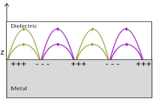
Figure 2. 4. E-field lines of Surface Plasmon Polaritons on a Metal- dielectrics interface.
12
2.1.3 Prism Coupling Scheme
Direct light cannot excite surface Plasmon polaritons on a metal/dielectric interface. This is due to the difference between the x-component of wave vector of light k, kx =k sinθ , and the SPP propagation constant β (x-direction is
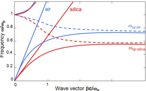
assumed to be the propagation direction of SPP-s). For interaction between the photons and plasmons to take place, conservation principles require they have equal energy and momentum. In figure 2.5 dispersion curves are seen to intercept only at the origin. Therefore in normal conditions this cannot be observed. Coupling techniques are needed to excite surface plasmons. Various alternative techniques are utilized to do the phase matching. The prism-coupling scheme is one of them. This is a three-layer system consisting of a metal film inserted between two different dielectrics; one of whose has the form of a prism. Kretschmann configuration is shown in figure 2.6 [Kretschmann and Raether, 1968] [8]. Total internal reflection occurs at the prism-metal interface. Note that surface plasmon excitation occurs only in the metal-air interface.
In the reflected beam intensity the SPP excitation can be recognized as a minimum in the beam intensity.
13
Figure 2. 6. Kretschmann configuration. SPP excitation occurs only at the metal-air interface.
14
Prism coupling can also be used to excite coupled surface plasmon polaritons(SPP) in MIM junctions. Another widely used phase-matching configuration is Otto geometry [9]. In this configuration the dielectric layer is placed between the prism and the metal. Total internal reflection (TIR) takes place at the prism-dielectric interface. Evanescent field tunneling across the dielectric layer excites surface plasmons on the metal-dielectric interface. Otto configuration is very uncommon because of its very sensitive property of dielectric layer thickness.
2.1.4 Grating Coupling Scheme
Another widely used technique to overcome the mismatch in wave vector between the in-plane momentum of the photons and β is the grating coupling scheme. Here a metal surface having an integrated grating is utilized. When light with wave vector ki falls on the grating, light gets diffracted. The diffracted
light’s wave vector 𝑘!"##,! then becomes:
𝑘!"##,! = 𝑘!,!+ 𝑚𝐺 (2.44)
where m is an integer and G is the grating vector along x-direction. The magnitude of the wavevector does not change if the difracted light does not change medium. Magnitude of the grating vector is:
𝑮 = 2𝜋
𝛬 (2.45)
Here 𝛬 is the period of grating used and 𝑮 is the grating vector.
As a condition of Plasmon exciting, the wave vector of diffracted light 𝑘!"##,! should be equal to the wave vector of the surface plasmons, 𝑘!". Therefore the
dispersion relation becomes:
𝑘!" = 𝑘!+ 𝑚2𝜋
15
16
2.2 Localized Surface Plasmons
Localized surface plasmons are non-propagating excitations of the conduction electrons of metallic nanostructures coupled to the electromagnetic field.
2.2.1 Localized Surface Plasmon Modes
Localized surface plasmon modes result from the solution of the problem of scattering of a sub-wavelength size conductive nanoparticle in an oscillating EM field. They are a consequence of the curved surface of the nanoparticle, which exerts a restoring force on the driven electrons. Restoring force is the reason of the resonance. Due to the resonance, field amplification is observed inside the particle and in the near zone outside the particle. Localized surface plasmons differ from propagating SPP. Due to the curved surface of the nanoparticles, localized surface plasmons can be excited directly by light illumination. In the propagating SPPs case, an additional prism is needed to excite the plasmon modes.
Now the case of a homogeneous, isotropic sphere in a uniform, static electric field E is considered (Figure 2.8). The sphere has a dielectric response described by the dielectric function ε(ω). The surrounding has a dielectric constant εm..
Solving Laplace’s equation and making use of Legendre’s polynomials (derivation details can be found at reference 7) yields a dipole moment p inside the sphere as follows:
𝒑 = 4𝜋𝜀!𝜀!𝑎!
𝜀 − 𝜀!
𝜀 + 2𝜀!𝑬𝟎 (2.47) If dipole moment is expressed as:
𝒑 = 𝜀!𝜀!α𝑬𝟎 (2.48)
Polarizability 𝛼 then becomes:
α = 4𝜋𝑎! 𝜀 − 𝜀!
17
Figure 2. 8. A conducting sphere under the effect of an electric field E. The medium is assumed to be air having an dielectric constant εm. [Adapted from
18
The condition that |ε+2εm| is a minimum would resonantly enhance polarizability. The Fröhlich condition is a result of the slowly varying imaginary part of ε(ω),:
𝑅𝑒[𝜀(𝜔)] = −2𝜀! (2.50) Modes associated with Fröhlich condition are called dipole surface plasmon of the metal nanoparticle. This relation is an indicator that the resonance frequency on the dielectric strongly depends on environment. This feature makes metal nanoparticles ideal to be used in sensing of changes in refractive index. Any change in environments refractive index changes the resonance.
The electric field distribution is evaluated from the potentials [7]: 𝑬𝒊𝒏 = 3𝜀! 𝜀 + 2𝜀!𝑬𝟎 (2.51) 𝑬𝒐𝒖𝒕 = 𝐸!+ 3𝒏 𝒏 · 𝒑 − 𝒑 4𝜋𝜀!𝜀! 1 𝑟! (2.52)
In this case both the internal and dipolar electric fields are enhanced. The resonant enhancement of the fields is due to the resonance in polarizability. Metal nanoparticles show interesting optical behavior. Light is efficiently absorbed and scattered in metal nanoparticles as a result of the resonantly enhanced polarization α. Pointing vector is used to calculate scattering and absorption cross sections Csca and Cab [18]:
𝐶!"# = 𝑘!
6𝜋 𝛼 ! (2.53)
𝐶!"# = 𝑘𝐼𝑚[𝛼] (2.54)
Substituting for 𝛼 in 2.53 and 2.54 yields: 𝐶!"# = 8𝜋
3 𝑘!𝑎!
𝜀 − 𝜀!
19
𝐶!"#= 4𝜋𝑘𝑎! 𝐼𝑚 𝜀 − 𝜀!
𝜀 + 2𝜀! (2.56) An important result of equations 2.55 and 2.56 is that for very small particles (a≪λ) the absorption efficiency is larger than scattering efficiency. As a result, a very small (~tens of nm) object is difficult to be imaged when neighbored by larger scatterers. Special techniques should be employed for imaging in such cases. Equations 2.55 and 2.56 also show that at the particle dipole Plasmon resonance, both absorption and scattering are enhanced.
2.2.2 Coupling of Localized Surface
Plasmons
Electromagnetic interactions between localized modes of neighboring nanoparticles cause additional shifts in Plasmon resonance. An array of one-dimensional nanoparticles is considered as the easiest case to be modeled and studied. Nanoparticles have size a and inter-particle distance d. They are considered to be close to each other (d≪λ). In this case near field interaction is dominant, having a distance dependence of d!!. Kren and his coworkers
experimentally studied the case, and in their setup a 1D array of metal nanoparticles was excited using a prism scheme. They observed strong field localization at interstitial sites, obtained by experimental results and supported by simulations. Scattering is suppressed for closely spaced particles.[19] These properties make inter-particle junctions very important in various applications where field enhancement is desired.
A model of interacting point dipoles is used to describe the situation. The particles are modeled as shown in figure 2.9. An incoming in-phase light polarizes the particles. Restoring force acting on the oscillating electrons will be affected by charge distribution of the neighboring nanoparticles. A blue shift is observed when incoming light excites transverse modes (2.9 a). If incoming
20
radiation excites longitudinal modes, red shift is observed (2.9b). Resonance shift is affected by geometrical parameters of the nanoparticle array: inter-particle distance and nanointer-particle length as well as polarization of the exciting light. If the particle separation is large, far-field dipolar coupling with a distance dependence of d−1 is dominant. [7]
21 a)
b)
Figure 2. 9. Near field coupling between near neighboring metal nanoparticles. Charge polarization caused by incoming light of two different polarization cases are shown. [Adapted from 7]
22
2.3 X-ray photoelectron spectroscopy
X-ray photoelectron spectroscopy (XPS) is one of the mostly used techniques in surface analysis and characterizing. Its working principle is based on the photoelectric process. An X-ray photon with energy hν is employed to eject an electron from the core level. The emitted photoelectron is used to do the analyzing, and the photoelectron spectrum is obtained in the form of a graph of intensity versus electron energy. The electron is identified by the binding energy, and its kinetic energy is employed as a mean to calculate the binding energy as following:
Here E! is the binding energy of the electron, hν is the energy of the incident x-ray photon, E! is the kinetic energy of the electron and Laser is the work function. All the quantities except E! are known, and binding energy can be
calculated. XPS provides information about the elements present at the surface, their chemical states, the portion of each chemical state and their spatial distribution. In cases when the material of interest is a thin film, XPS can provide information regarding the film thickness, uniformity of the thickness and uniformity of the chemical composition of the film. [10]
23
hυ
e
-‐
E
k(e
-‐) = hυ-‐ E
b24
2.4 Metal-Insulator-Metal Junctions
The samples studied in the following chapters are basically MIM diodes. Here a short description of the working mechanism, electrical properties and plasmonic effects in MIM structures will be given.
2.4.1 Basics of Metal-Insulator-Metal
Junctions
In Metal-Insulator-Metal structures two metals are joined by an insulator sandwiched in between.
Energy band structure of MIM is determined by the following quantities: • work functions of each of the metals Φ! and Φ!,
• electron affinity of insulator χ • bandgap of the insulator
With these values known, the band diagram of the MIM structure at equilibrium can be visualized as in figure 2.11. In figure 2.11a, same metal (Ag) is used in both sides of the insulator.
25
Figure 2. 11. Band diagrams of ideal MIM junctions. At diagram a) same metals are used and at b) different metals are used. Equilibrium is assumed at both cases. Bent of the vacuum energy band due to applied voltage is not shown.
26
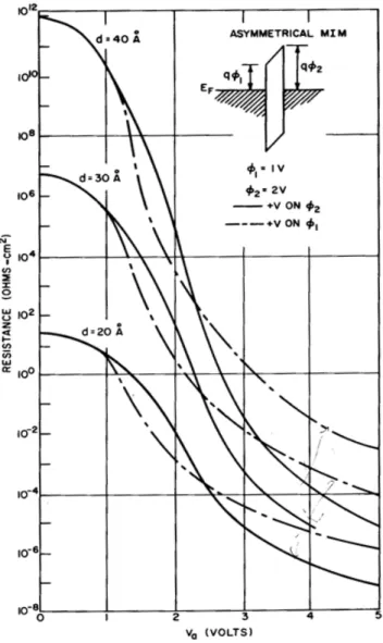
Figure 2.12. Theoretical Tunnel Resistance as a Function of Applied Voltage for an Asymmetrical MIM Structure. [11]
27
In the diagram shown in 2.11b, different metals (Ag and Al) were used to sandwich the insulator layer. Here a build-in electric field will appear at equilibrium conditions, bending the energy band diagram of the insulator. At figure 2.12 the tunnel resistance as a function of V for d = 20, 30 and 40A, Ф
1 = 1V, and Ф 2 = 2V is illustrated. [11]
Barrier height and width are determinant factors in the tunneling probability of the electron through the barrier. The transmission probability is given by the Schrödinger Wave equation [12],
𝐷 = 𝑒𝑥𝑝 (−2𝑑 [2𝑚 (𝑉 − 𝐸)/ћ! ] !/! ) (2.59)
Here, V is the barrier height and E is the energy of the particle. D is the transmission probability and d is the thickness of the insulator. As can be inferred from 2.48, electron tunneling becomes less common as thickness of the insulator increases. When different metals are used to sandwich the insulator layer asymmetry is noticed in the behavior of the diode under forward and reverse bias. This is due to the difference in the work functions of the two metals. If current flows only due to tunneling of electrons across the diode, i.e. we are dealing with a tunneling diode, in the forward bias case the road an electron has to travel through the potential barrier is shorter than in the reverse bias case. Therefore more electrons will pass the barrier and contribute to the current in the forward bias than there will be in the reverse bias. The performance of a diode is strongly limited by the difference in the work functions of the two metals. Using metals with different work functions improves the performance of a diode. [13]
28
Figure 2. 13. Energy band diagram of MIM junctions under different bias conditions. From left to right: No bias, Reverse Bias, Forward Bias. [13]
29
2.4.2 Plasmonic Effects in MIM
Structures.
MIM structures are multilayers consisting of an insulator layer sandwiched between two metal layers. The structure hosts two metal-insulator interfaces in the middle (the metal layers are considered to be semi-infinite).
Both interfaces host SPPs that decay perpendicularly to the surface with a decay length depending on the material properties of the metals and the insulator. When the thickness of the insulator layer is smaller than or comparable to the decay length of the interface mode, interactions between SPPs of the two interfaces gives rise to coupled modes.
The field components for non–oscillatory TM modes in the z-direction (schematically shown in figure 2.14) are described as follows:
For z > a : 𝐻! = 𝐴𝑒 !"#𝑒!!!! (2.60) 𝐸 ! = 𝑖𝐴! 1 𝜔𝜀!𝜀! 𝑘!𝑒!"# 𝑒!!!! (2.61) 𝐸 ! = −𝐴! 𝛽 𝜔𝜀!𝜀! 𝑒!"# 𝑒!!!! (2.62) For z < −a 𝐻! = 𝐵𝑒 !"#𝑒!!! (2.63) 𝐸 ! = −𝑖𝐵 1 𝜔𝜀!𝜀! 𝑘!𝑒!"# 𝑒!!! (2.64) 𝐸 ! = −𝐵 𝛽 𝜔𝜀!𝜀! 𝑒!"# 𝑒!!! (2.65)
30
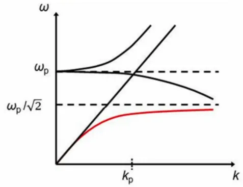
Figure 2.14. Dispersion plot for MIM structure [20]
Figure 2.15. MIM structure geometry. The coordinative system shown is used in derivations.
31
Fields in regions II and III are expected to decay exponentially. Modes localized at both the interfaces couple at the insulator. The vector component of each field can be added to yield:
𝐻! = 𝐶𝑒!"#𝑒!!!+ 𝐷𝑒!"#𝑒!!!! (2.66) 𝐸 ! = −𝑖𝐶!!! !!! 𝑘!𝑒 !"#𝑒!!!+ 𝑖𝐷 ! !!!!! 𝑘!𝑒 !"#𝑒!!!! (2.67) 𝐸 ! = 𝐶 𝛽 𝜔𝜀!𝜀! 𝑒!"#𝑒!!!+ 𝐷 𝛽 𝜔𝜀!𝜀!𝑒!"#𝑒!!!! (2.68)
Using of the continuity of Laser and Ex at the interfaces z=a and z=-a , the
dispersion relation is obtained after solving the set of linear equations.
If the top and bottom metals are of same material, the dispersion relation can be expressed as:
tanh 𝑘!𝑎 = −𝑘!𝜀!
𝑘!𝜀! (2.69)
tanh 𝑘!𝑎 = −𝑘!𝜀!
𝑘!𝜀! (2.71)
Equation 2.70 and 2.71 show the odd and even vector parities respectively. In the odd vector parity case Ex(z) is odd, Laser(z) and Ez(z) are even functions. In
the even vector parity Ex(z) is even function Laser(z) and Ez (z) are odd
functions. The equations derived so far were general for multilayer structures. For the MIM case, ε2 =ε2(ω) is the dielectric constant of the metal, considering
same metal in used in the top and bottom contacts, and ε2 is the dielectric
constant of the insulator. If top and bottom metals are not made of same material, the coupling between SPP modes at the two interfaces changes a lot
𝑒!!!!! = 𝑘! 𝜀!+ 𝑘! 𝜀! 𝑘! 𝜀 !− 𝑘! 𝜀! 𝑘! 𝜀!+ 𝑘! 𝜀! 𝑘! 𝜀 !− 𝑘! 𝜀! (2.70)
32
because of the metals different dielectric constants. The difference in dielectric constant will prevent the phase matching [21]. Coupling in both cases is a strong function of the insulator thickness, and with the insulator becoming thicker the coupling will fade after a certain point.
2.4.3 QM Tunneling Mechanisms in MIM
Structures.
Quantum mechanical tunneling describes the transition of carriers through energy state classically forbidden. In the case of the MIM structures the forbidden energy state is insulator bandgap. According to classical mechanics, the probability that the particle passes through the energy barrier is zero. However, due to the wavelike behavior of particles on the quantum scale, quantum mechanics predicts a probability value, even though small, for the particle to be on the other side of the barrier. Direct tunneling, Fewler-Nordheim tunneling and trap-assisted tunneling (TAT) are the tunneling mechanisms mostly affecting tunneling current. In direct tunneling electrons propagate through the barrier without using the conduction band of the dielectric. Direct tunneling is temperature dependent and it increases exponentially with decreasing oxide thickness. The most important characteristic of direct tunneling is that it does not create oxide defects after repeated cycle operations, leaving the oxide structure unaffected [15]. Fowler-Nordheim Tunneling is a special case of direct tunneling (Figure 2.16b). Here electrons tunnel from one side of the insulator to the other side by passing the conduction band of the oxide. Trap-assisted tunneling becomes significant after a large number of carriers have passed through the dielectrics creating defects in its structure. Only one defect would not create a large leaking current, but many defects would deter the performance of the MIM device. [16]
33
a) b) c)
Figure 2. 16. Schematic view of tunneling mechanisms. a)Direct tunneling, b)Fowler-Nordheim Tunneling, c)Trap-assisted Tunneling [14]
34
Chapter 3
Hot-electron and Plasmonic effects in
Metal-Insulator-Metal structures.
In the previous chapters a theoretical review of Surface Plasmon, X-ray photoelectron Spectroscopy and metal-insulator-metal junction were given. In this chapter a detailed review of recent studies of plasmonic and hot electron effects in MIM structures is provided. MIM junctions are used in applications such a photodetectors and energy harvesting devices. MIM junctions are fabricated by well known, simple and controllable thin film deposition techniques. This feature is desirable for engineers and it makes MIM more attractive for applications. Understanding and modeling the effect of surface plasmons and hot electrons in MIM structures is hence very important. Lately a number of papers on this topic have been published, and many groups are trying to fully understand the theory laying behind. When photons hit an MIM junction each photon excites an electron at the metal, giving it energy and depending on the energy the electron may or may not excite over the Fermi level. If kinetic energy of the excited hot electron exceeds insulator barrier, there is a probability for the electron to travel through the insulator and contribute to the current. Different models have been proposed to model the hot electron behavior at MIM sandwiched structures. Recently Chalabi et al [3] used a 5-step model to describe the photoemission of electrons across a barrier. Their approach was based on the earlier method used by Spicer [22]. In their work, Chalabi and her coworkers reshaped one of the metallic contacts in the MIM structure, so that it supported plasmonic resonances. Hence they enhanced the efficiency by using one of the contacts as antenna that resonate Surface Plasmon Polaritons. The device they used consisted of an Au metallic substrate coated by a layer of Al2O3. Top Au
layer was shaped by means of lithography. The 5-step model is shown in figure 3.1.
35
Figure 3.1. Photocurrent caused by electrons passing through the barrier. Photoelectrons are excited at the top and bottom metals as well, so backward current will be produced even if less than the forward current. Here a voltage has been applied.[3]
36
In the first step hot electrons are generated in the top metal and excited to an energy level equal to the incoming photon. Here an important assumption is made. The electrons in the metal are assumed to behave as free electrons, and the energy gained by interaction with the photon goes totally to kinetic energy used to “lift” the photon in the band diagram. Also the electrons momentum is assumed to be equally distributed in all directions; isotropic. At step 2, statistically half of the electrons will move towards the metal-insulator interface. Only a small fraction of those make it to the interface. Many will lose their energies in inelastic interactions. The fraction of electrons arriving to the interface can be found by making use of the mean free path of energetic electrons in solids. Step 3 is at the interface. If the electron has kinetic energy smaller than the barrier, there is a small probability that it will tunnel according to quantum mechanics. Even if the electrons kinetic energy is larger than the barrier and enough to pass it, the probability for the electron to inject into the oxide will still be small due to the contrast in wave vector between the injected electrons and the oxide electrons. While passing through the oxide there is a certain probability that the electron will pass without inelastically colliding and make it to the next interface and this is step 4. In step 5, at the junction between the insulator and the bottom metal reflection is possible due to the mismatch in wave vectors.
Further, Chalabi et al and her coworkers have experimentally studied the voltage-dependence, spectral-dependence, stripe-width dependence and polarization-dependence of the photocurrent in the device.[2] The materials used are Au-Al2O3-Au. This makes device’s potential band diagram to be symmetrical under equilibrium conditions. According to optical simulations, light of the light is absorbed at the top stripe that at the bottom metal (at least 1 order of magnitude difference). Due to the asymmetric absorbance of light in the two metals, even at 0V bias forward current is larger than the backward current and a net photocurrent has been observed. To show the effect of plasmonic enhancement in the photocurrent, they have fabricated samples with different stripe width and compared their electrical properties. Also a polarizer has been
37
employed to provide TM and TE polarized light. It has been observed that the photocurrent for the TM polarized light was much larger than for the TE polarized light falling on the strips. The explanation provided is related to excitation of SPP-s in the grating- oxide interface by the TE polarized light. [2]
Wang and Melosh et al also demonstrated theoretically and experimentally that
hot electrons excited in the metal electrode could be collected and converted into solar energy by using a MIM structure. They described the hot electron-Plasmon effect, and proposed that the detrimental nature of surface electron-Plasmon decay in fact can be used to boost energy conversion. The metal film is utilized to absorb light and emit electron at the same time, and the electron energy is harvested before converting to heat.
They have studied the effect of the thickness of the upper metal on the current. An optimal thickness exists. If the metal is too thick, more photons would be absorbed but there is a longer way for the electrons to reach the metal-insulator interface. The probability that electron would scatter is therefore larger. On the other hand, absorbance in thin metal layers is poor.
Even though most of the electrons would make it to the interface, poor absorbance leads to many reflected photons, and not enough photons are absorbed to excite the electrons. Kretschmann geometry has been used to excite SPs hand it is compared to the case when direct illumination was used.[2]
38
Figure 3. 2 Energy diagram of the MIM device. Electrons are excited to higher energy states (hot electrons) incoming photons with energy hγ. Hot carriers are excited in the top and bottom metal as well. [2]
Figure 3.3. Mechanism of hot electron transmission in MIM devices in cases when excitation of SPs and direct illumination. [2]
39
The probability that an hot electron reaches the interface is proportional to: exp[-d/(λecosθ)]. Here d is the metal thickness; λe is the mean free path of the electron
in the metal. For Silver the mean free path of an electron having a kinetic energy of 1.96eV is 56 nm. [2],[23]
MIM device can be adjusted to absorb light at any wavelength. The system can be set that only the hot electrons above the barrier generate power. Both the open circuit voltage and short circuit current can be tuned by changing the thicknesses of top and bottom metal layers. [24]
Melosh et al has also used MIM devices to determine the wavelength of
monochromatic light in a power-independent fashion. The main promising feature of this device is that the ballistic electron transport is very fast, in the range of picoseconds; hence the device is thought to work good even at high frequencies. The open circuit current of the device is independent of the device area, therefore the device can be scalable to nanometers sizes. The open circuit voltage, Voc can be calculated as follows [2]:
𝑉!" = 𝐸!!− 𝛷! 𝑒 1 −
𝐼!"!"#
𝐼!"!"# (2.1)
Here 𝐸!! is the energy of the photon, 𝛷! is the barrier for the electron and 𝐼!"!"#
and 𝐼!"!"# are the short circuit currents for the top and bottom metals. If
𝐼!"!"# ≪ 𝐼
!"!"#, the second bracket of equation 3.1 can be approximated to be 1,
and equation 3.1 takes the following form:
𝑉!" = 𝐸!!− 𝛷!
40
Chapter 4
Fabrication and Characterization of
Plasmonic Surfaces
In this chapter the design, fabrication and characterization techniques used will be described. The devices fabricated and used here can be divided in two categories. In the first category, Silver nanoparticles were deposited on an insulator layer, that itself was deposited at different thicknesses on a metal substrate. Different materials were used for both the bottom metal layer and the insulator. We worked towards optimizing the optical properties of the substrates. We aimed to achieve high light absorption. Indeed, at a defined combination of the insulator thickness, Ag nanpoparticles size and distribution, almost perfect absorption of light was achieved at visible spectra (350-750nm).
The second category is similar to the first but differs in the fabrication methods used and the form of the top metal layer. Here, instead of the nanoparticles with random distribution and size used in the first case, metal gratings with well defined geometry were patterned and deposited on the insulator layer.
Atomic layer deposition (ALD) and thermal evaporation were used to deposit the insulator layer and the metal layers respectively. All fabrication processes are conducted in Class100 clean room facility at UNAM.
Atomic Layer Deposition
Atomic Layer Deposition is a Chemical Vapor Deposition technique. In ALD the precursors are pulsed into the reactor alternately, one at a time. During one pulse, firstly the first precursor is exposure. After that, purge or evacuation of the reaction chamber occurs. A purging or evacuation periods is needed between each precursor pulse to clean the sample from the first precursor and prepare it for the other precursors. Exactly the same process is repeated for the second precursor.
41
42
In this manner, this process is repeated as many times as needed to obtain the thickness aimed. The number of pulses needed to obtain a film of a certain thickness can be precisely determined. This is due to self-limiting property of ALD. Each cycle grows exactly one monolayer. The greatest advantage of ALD is the uniformity of the deposited film. This is due to the self-limiting growth mechanism of ALD. This feature of the ALD grown insulator films gives confidence about the electrical insulating of the oxide layer, and the probabilities that there will be some leakage of current through the insulator becomes minimal. Insulating layers of HfO2 and Al2O3 were deposited by ALD.
Thermal Evaporation
Making use of the VAKSIS PVD Vapor-3S Thermal Evaporation System bottom metal layer is formed. At the process, metal is heated to several hundreds of degrees in a vacuum environment. When evaporation temperature is reached, vapor particles from the source move towards the sample and condense to a solid state on the surface. The chamber is at vacuum so the probability that the vapor particles collide on the way towards the substrate is minimal. The main parameters of thermal evaporation systems are:
• Chamber pressure • Substrate temperature
• power applied to source material
• the distance between the source and the substrate.
Thermal evaporator is widely used in microfabrication for making metal contacts. An advantage of thermal evaporation system is that different layers can be deposited without breaking the vacuum. This allows for clean process and reliability of the sample. A wetting layer of 3 nm Germanium is deposited first on the silicon wafer. The silicon substrates are chosen to be undoped so that they provide an insulating environment and do not affect the electrical properties of the MIM structure on them. Without opening the chamber, on the wetting layer
![Figure 2. 16. Schematic view of tunneling mechanisms. a)Direct tunneling, b)Fowler-Nordheim Tunneling, c)Trap-assisted Tunneling [14]](https://thumb-eu.123doks.com/thumbv2/9libnet/5961819.124577/54.892.164.750.282.563/schematic-tunneling-mechanisms-tunneling-nordheim-tunneling-assisted-tunneling.webp)
![Figure 4. 1. Savanah Atomic Layer Deposition system at UNAM [25]](https://thumb-eu.123doks.com/thumbv2/9libnet/5961819.124577/62.892.173.750.308.682/figure-savanah-atomic-layer-deposition-system-at-unam.webp)