RF-SPUTTERING OF DOPED ZINC OXIDES
THIN FILMS, THE EFFECT OF LOW
SUBSTRATE HEATING DEPOSITION
A THESIS SUBMITTED TO
THE GRADUATE SCHOOL OF ENGINEERING AND SCIENCE OF BILKENT UNIVERSITY
IN PARTIAL FULFILLMENT OF THE REQUIREMENTS FOR THE DEGREE OF
MASTER OF SCIENCE IN
MATERIALS SCIENCE AND NANOTECHNOLOGY
By
Amira Ahmed Abdelmoneam Mohamed Ahmed January, 2017
RF-SPUTTERING OF DOPED ZINC OXIDES THIN FILMS, THE EFFECT OF LOW SUBSTRATE HEATING DEPOSITION
By
Amira Ahmed Abdelmoneam Mohamed Ahmed Jan 2017
We certify that we have read this thesis and that in our opinion it is fully adequate, in scope and in quality, as a thesis for the degree of Master of Science.
_______________________________ Aykutlu Dana (Advisor)
_______________________________ Necmi Biyikli (Co-Advisor)
_______________________________ Raşit Turan
_______________________________ Talip Serkan Kasirga
Approved for the Graduate School of Engineering and Sciences:
_______________________________ Assoc. Prof. Dr. Ezhan Karaşan Director of the Graduate School
I
ABSTRACT
RF-SPUTTERING OF DOPED ZINC OXIDES THIN FILMS, THE
EFFECT OF LOW SUBSTRATE HEATING DEPOSITION
Amira Ahmed Abdelmoneam Mohamed Ahmed M.S. in Materials Science and Nanotechnology
Advisor: Assist. Prof. Dr. Aykutlu Dana
Jan, 2017
Zinc Oxide (ZnO) has been studied since 1930’s as a candidate for the electronic
applications, as it possesses a wide bandgap of 3.4 eV. While in the last 3 decades the technology of thin films were more interested in Doped zinc oxide (ZnO) for their promising potential for many applications including thin film transistors (TFTs), transparent conductive electrodes (TCEs), and thin-film photovoltaic solar cells. Mainly Indium doped and Gallium doped-zinc-oxide (IZO), (GZO) and (IGZO) thin films have drawn researchers’ attention due to their remarkable electrical, optical properties, making them good candidate for the next generation flexible optoelectronic applications.
This thesis work studies the effect of deposition parameters on the crystallinity and optical properties of the thin films. In addition, the chemical composition, electrical and morphological properties of the thin films were studied in a comparative form between room temperature (RT)-grown thin films and those gown with substrate heating at 200 °C. First, a series of doped ZnO thin films were deposited by radio frequency RF-sputtering at (RT), as a function of pressure, plasma power, and argon (Ar) flow. Then a chosen deposition recipe was tested with substrate heating. Well-adhered, uniform, smooth and highly transparent films were observed. Although Literature has shown that IZO thin films exhibit amorphous nature at RT-deposition, in this work it was observed that IZO thin films exhibits crystalline nature at RT. Results indicated that low substrate heating has affected both of IZO and GZO more than it has to IGZO Thin films. The low heat effect was more effective on the
II
crystallinity and optical characteristics of these thin films more than its effect on their other characteristics, as it will be demonstrated as we go over each characteristic. Thicker films of (~1m) were grown in order to evaluate the mechanical properties, including film hardness (H) and Young’s Modulus (E).
Keywords: RF-Sputtering, Doped-Zinc-Oxide, Indium Gallium Zinc Oxide, Thin
III
ÖZET
RF- PÜSKÜRTMELİ KATKILANMIŞ ÇİNKO OKSİT İNCE
FİLMLER, DÜŞÜK ALTTAŞ ISITMALI BÜYÜTME ETKİSİ
Amira Ahmed Abdelmoneam Mohamed Ahmed M.S. in Materials Science and Nanotechnology
Advisor: Assist. Prof. Dr. Aykutlu Dana
Jan, 2017
Çinko oksit (ZnO) 3.4 eV gibi geniş bir bant aralığına sahip olması ile beraber,
1930’lu yıllardan beri elektronik uygulamalar için kullanılmaktadır. Son otuz yıl boyunca ince film teknolojileri, ince film tranzistörler (TFTs), şeffaf iletken elektrotlar (TCEs) ve ince film fotovoltaik güneş hücreleri gibi uygulmalarda daha çok potansiyel vadetmesi sebebiyle, katkılanmış çinko oksit ile daha fazla ilgilenmektedir. Özellikle indiyum ve galyum katkılı çinko oksit (IZO), (GZO), (IGZO) ince filmler dikkate değer elektriksel ve optik özelliklerinden dolayı araştırmacıların daha çok ilgisini çekmekte ve yeni nesil esnek optoelektonik uygulamalar için iyi bir aday olarak göze çarpmaktadır.
Bu tez çalışması, ince filmlerde, kaplama parametrelerinin, optik özellikler ve kristallik üzerindeki etkisini incelemektedir. Ayrıca, ince filmlerin, kimyasal bileşimleri, elektriksel ve şekilsel özellikleri oda sıcaklığında ve 200°C alltaş sıcaklığı altında büyütülen filmlerde karşılaştırmalı olarak çalışıldı. Öncelikle, basınç, plasma gücü ve Argon (Ar) gaz akışı gibi kaplama parametreleri farklı değerlerde değiştirilerek, katkılandırılmış ZnO filmler seri olarak RF- püskürtmeli kaplama tenkiği ile kaplandı. Sonrasında seçilmiş bir kaplama reçetesi alttaş sıcaklığı değiştirilerek test edildi. İyi yapışmış, eş dağılımlı, pürüzsüz ve yüksek oranda saydam filmler gözlendi. Literatür IZO ince filmlerin oda sıcaklığında kaplandığında amorf bir yapıya sahip olduğunu sölese de, bu çalışmada oda sıcaklığında kaplanan IZO ince filmlerin kristal bir yapıya sahip olduğunu gösterdi. Sonuçlar, kaplama esnasında alttaşın düşük miktarlarda ısıtılmasının hem IZO hem de GZO ince filmlerde IGZO ince filmlere oranla daha etkili olduğunu gösterdi. Her bir karakterizasyon aşamasının ayrı ayrı bahsedilecek olmasıyla beraber, düşük
IV
sıcaklığın, diğer karakterizasyonlara kıyasla; kristallik ve optik özelliklerde daha çok etkili olduğu gözlendi. Kalın filmler (~1 µm), film sertliği (H) ve elastikiyet katsayısını (E) içeren mekanik özelliklerin incelenmesi için büyütüldü.
Anahtar Kelimeler: RF-Püskürtme, Katkılı-Çinko-Oksit, Indiyum Galyum Çinko
V ميحرلا نمحرلا الله مسب " ۚ ااهاع ْس ُو هلَِإ اًسْفان ُ هالله ُفِّلاكُي الَ ااهال اام ْتاباساك ااهْيالاع او اام ْتاباساتْكا " ( ةيلاا , ةرقبلا ةروس 286 )
"God does not impose on any soul a responsibility beyond its
ability. Every soul receives whatever it gains and is liable for
whatever it does"
)Al-Baqra Verse No:286(
That’s how I know, that whatever obstacle I face, or whatever
struggle is set upon me, I have the power to handle and manage
the situation no matter what.
VI
Acknowledgement
First, I’d like to thank the jury committee; Prof. Turan Raçit and Dr. Serkan Kasigra for their fruitful comments and guidance.
Special Thanks to my advisor Prof. Aykutlu Dana, for his support during the crisis I have faced here in UNAM, and for accepting me in his group. Also, thanks to my Co-advisor Prof. Necmi Biyikli.
Thanks to Dr. Eda Goldenberg for giving me the chance to get this thesis done through her project entitled “Development of ZnO Based Transparent Conducting Metal Oxides for Next Generation Applications on Flexible Substrates” funded by TUBITAK
Thanks to all my group mates Seda Kizir, Ali Haider and Turkan Bayrak for their help in this project and for sharing their knowledge.
Special thanks to my dear friends; Gulbahar Saat, Ahmed Oaf, Nour Almadhoun, Mohammed H. Alser and Zahraa Ghanem for their continuous support and for being there when I needed help the most, thanks for being in my life.
Thanks for my office mates, specially, Begimai and Ali Kalantari for his repetitive question “did you finish?” which kept me alert to finish as fast as I can just not to hear this question again, thanks for the motivation.
Huge Thanks to the one person in UNAM who made our life (foreigner students) in here a lot easier, Thanks to Duygu Kazancı for her sweet, kind and continuous support.
Thanks to Dr. Mehmet Yilmaz, and Dr. Peter for sharing their knowledge.
Thanks to my good friends; Talha Masood Khan and Murat Serhatlioglu for their help and support. Thanks Murat for translating the abstract into Turkish.
VII
I’d like to express my sincere gratitude to my mentors; Dr. Mostafa El-Ashry, Dr. Osama Tobail and Dr. Sherif Abbas, I wouldn’t be here if not for your support and encouragement, May Allah always grant you success and happiness always.
Heartwarming thanks to my friends for life, I love to call it “The Sisterhood of The Traveling Researcher”. Although we are scattered all over the world chasing after our dreams, working our hearts out for our families and for our studies and research, we never let go of each other’s. Sadness or happiness, joy of grief, stressed or relaxed we have been always there for each other and still. Thanks to you gals, Nayyera Fouad, Mai Ibrahim, Ghada Antar, Mona Atta, Ghada Hamdi and Nahla Abdelshafi. No matter the distance, we will be always together. Nayyera, you are a life saver, we are all lucky to have you in our lives.
Thanks to Nashwa Moatez, Samah Elmahdy and Asmaa Foaud, I’ve learnt a lot from you and all of you mean a lot for me. I’m so happy that by the time I defended this thesis, Samah just got her master’s too. Maybe I’m the only one, who is always away, but you are always in my heart, May Allah blesses us with this special friendship forever and always.
Mam and Dad, this is for you, I would be nothing if not for your unconditional love and support. Sorry, for the sleepless night you endured for me, so I can achieve my goals and dreams. Sorry, for the times I missed to be with you. Sorry for every call I missed form you because of work and meetings. No enough “sorry” and definitely No enough “thanks” can be appreciative enough to what you have sacrificed for me and my sister and brother. This is for you Mam and Dad.
VIII
To Mam & Dad
To Sis & Bro
To you T & U ;)
IX
Contents
ABSTRACT ... I ÖZET... III Acknowledgement... VI List of Figures ... XI List of Tables... XIII1. Introduction ... 1
1.1. Doped Zinc Oxide Thin Films ... 3
1.2. Film Deposition and Fabrication ... 3
1.3. Motivation ... 6
1.4. Thesis Overview ... 7
Experimental Methodology ... 8
2. 2.1. Sputtering ... 9
2.1.1. Thin Films Deposition ... 10
2.2. Thin Film Characterization Techniques ... 13
2.2.1. Optical and Electrical Characterization ... 13
2.2.2. X-ray Diffraction (XRD)... 15
2.2.3. X-ray photoelectron spectroscopy (XPS)... 16
2.2.4. Atomic Force Microscopy and Nano-Indentation... 17
Results and Discussion ... 19
3. 3.1. Indium Zinc Oxide Thin Films (IZO) ... 20
3.1.1. Crystallinity and Optical properties ... 20
3.1.2. Chemical Composition, Bond State and Electrical properties ... 27
X
3.2. Gallium Zinc Oxide Thin Films (GZO) ... 31
3.2.1. Crystallinity and Optical properties ... 31
3.2.2. Chemical Composition and Electrical Properties ... 44
3.2.3. Morphological Structure ... 46
3.3. Indium Gallium Zinc Oxide Thin films (IGZO) ... 48
3.3.1. Crystallinity and Optical properties ... 48
3.3.2. Chemical Composition, Bond State and Electrical properties ... 53
3.3.3. Morphological Structure ... 55
3.4. Mechanical Characteristics of the Doped Zinc Oxide Thin Films; IZO, GZO and IGZO ... 56
Conclusion and future prospective ... 58
4. Bibliography ... 61
XI
List of Figures
Figure 1.2-1 A diagram showing the Thin Films Deposition Techniques ... 5
Figure 2.2-1 Bragg’s diffraction ... 15
Figure 2.2-2 Schematic illustration of indentation load- displacement data ... 17
Figure 3.1-1 XRD Pattern of RT-grown thin films of IZO ... 21
Figure 3.1-2 XRD Pattern of IZO thin films at different process pressures ... 22
Figure 3.1-3 XRD patterns of IZO thin films grown under RT and 200 °C ... 23
Figure 3.1-4 IZO thin films refractive indices ... 25
Figure 3.1-5 Extinction Coefficients (k) of IZO Thin Films ... 25
Figure 3.1-6 Transmission Spectra of IZO Thin Films ... 26
Figure 3.1-7 IZO thin film 2D AFM images, a) RT-grown, b) 200 °C ... 30
Figure 3.2-1 XRD Pattern of GZO thin films Deposited at different RF powers ... 33
Figure 3.2-2 XRD Pattern of GZO thin films Deposited at different pressures ... 33
Figure 3.2-3 XRD Pattern of GZO thin films Deposited at different (Ar) flow ... 34
Figure 3.2-4 XRD Pattern of GZO-wt5% thin films of different thickness... 34
Figure 3.2-5 XRD Pattern of GZO-7wt% thin films depsoited at 100 and 150 watt ... 35
Figure 3.2-6 Plot of (αhν)2 versus (hν) to estimate the bandgap by extrapolation ... 37
XII
Figure 3.2-8 Transmission Spectra of GZO-7wt% thin films group ... 39
Figure 3.2-9 XRD patterns for GZO-wt5% as-deposited and Substrate heating ... 41
Figure 3.2-10 XRD Patterns of GZO-7wt%, at RT and 200 °C deposition ... 42
Figure 3.2-11 Transmission Spectra of GZo-5wt% grown in (RT) and 200 °C ... 43
Figure 3.2-12 2D AFM images of GZO-7wt% GZO-5wt%, a) RT-grown, b) 200 °C ... 47
Figure 3.3-1 XRD Patters of IGZO Thin Films at RT and 200°C deposition ... 49
Figure 3.3-2 Refcractive Indices of IGZO thin films ... 51
Figure 3.3-3 Extinction Coefficients (k) of IGZO Thin Films ... 52
Figure 3.3-4 Plot of (αhν)2 versus (hν) for IGZO ... 52
Figure 3.3-5 Transmission Spectra of IGZO as a function of growth temperature ... 53
XIII
List of Tables
Table 2.1-1 IZO Deposition Parameters ... 12
Table 2.1-2 GZO-5wt%- Deposition Parameters ... 12
Table 2.1-3 GZO-7wt%-Deposition Parameters ... 12
Table 2.1-4 IGZO- Deposition Parameters ... 12
Table 3.1-1 Optical Bandgap and Transmission of IZO Thin Films ... 24
Table 3.1-2 Transmission Spectra of IZO Thin Films ... 28
Table 3.1-3 IZO thin films Electrical Properties ... 28
Table 3.2-1 GZO Thin Films Optical Bandgap (Eg) ... 37
Table 3.2-2 Optical Bandgap (Eg) and electrical characteristics of GZO thin films ... 45
Table 3.3-1 IGZO Thin Films Optical Bandgap ... 51
Table 3.3-2 IGZO Thin Films Electrical Properties... 54
Table 3.4-1 Electrical Properties of the doped-ZnO thin films ... 57
Table 4.1 Effect of Deposition Parameters on the Doped-ZnO Thin Films ……... 59 Table 4.2. Effect of Substrate Heating on the Doped-ZnO Thin Films Characteristics…60
1
Chapter 1
Introduction
1. Introduction
Z. R. Dai et al in one of the reviews stated that “Functional Oxides are the fundamentals of the smart devices”[1]. No wonder in that, since most of the nano-electronics technologies are depending on one or more of the functional oxides materials, this is not only because of their unique optical, electrical and chemical properties; but also the capability to tune these characteristics which is an application dependent request. Such characteristics make the functional oxides a diversified group of materials; that has its beneficence in many research aspects such as Superconductivity, semiconductor physics ferroelectricity and Piezoelectricity. Most studied materials are; SnO2, In2O3, Ga2O3, ITO, CdO, PbO2 and the different
types of the doped ZnO including; AZO, GZO, IZO and IGZO[1,2]. Each of these functional oxide materials is specifically recognized for certain property. For example in terms of transparent conductive oxides (TCO), ZnO:F and Cd2SnO4 are
recognized as highest transparency, while In2O3:Sn is recognized as the highest
2
Functional oxide materials are fabricated and synthesized into many different structures and phases, depending on the fabrication methods and parameters. Such structures includes; nano-belts, nanowires, nano-sheets, and nano-diskettes[1,4–6]. Generally, the material studies of the functional oxides revolves around two aspects; first, the synthesis and fabrication methods and processes, second, the characterization of the fabricated or synthesized structures, to quantify their characteristics which in turns give insights about their proposed potential applications.
Taking that Thin films is the main focus of this work, it’s convenient to shed some light on the thin film history. Starting at 1950’s the thin films materials have undergone an extensive major studies that focused on their characteristics, investigating their ability to be integrated into the electronic applications and devices. That in turns, by 1960’s, led to the first thin film transistor (TFT) proposed by Weimer, where he used CdS as a semiconductor thin film. As a result, more applications were proposed by 1970’s; introducing novel thin film devices such as surface acoustic wave (SAW) devices and thin-film integrated optics. The silicon technology by that time has shown a promising results regarding (a-Si)-based (TFT) and a-Si solar cells. During the 1980’s a speedy progress in the a-Si technology was observed as a result; a-Si solar cells were integrated into the electronic calculators as well as liquid crystal television[7].
In this work the focus is mainly on the doped zinc oxide thin films deposited by RF-Sputtering and the effect of the deposition parameters on their characteristics. Moreover, the effect of the low substrate heating deposition and its ability to be effective as the annealing process, which in turn will reduce the processes used.
3
1.1. Doped Zinc Oxide Thin Films
Fritsch in 1935 has fabricated polycrystalline Zinc oxide films, however not till 1960’s were ZnO thin films were heavily studied, to investigate the their capabilities as piezoelectric material for acoustic wave devices[8]. Since then, ZnO have drawn the attention of the many researchers because of its remarkable optoelectronics characteristics that led them to be recognized as a promising candidate for many applications especially for transparent conductive electrodes that are for solar cells, light emitting diode (LED) and flat panel displays (FPDs)[9–12]. Over the other materials, ZnO thin films gets attention with its high transparency in the visible region (>85%), low cost, source availability, along with non-toxicity[13,14]. However, stoichiometric ZnO exhibits relatively high resistivity due to low carrier concentration and low carrier mobility[15,16]. Recently it is shown that IGZO-based thin film transistors (TFTs) are considered as a replacement for their conventional counterparts[17]. Thin films of Ga and In-Ga doped ZnO have been grown by a variety of deposition processes, including sol-gel[18,19], metal-organic chemical vapor deposition (MOCVD)[20], pulsed laser deposition[21,22], and dc and/or RF-magnetron sputtering[23,24]. Within all these techniques, RF-RF-magnetron sputtering offers highly uniform and well-adhered thin films on large area substrates with high packing density even at low deposition temperatures. In general, it is known that the film structure, composition, electrical and the optical characteristics might be affected by the deposition parameters including (RF) plasma power, gas flow, working pressure, chamber geometry and substrate temperature.
1.2. Film Deposition and Fabrication
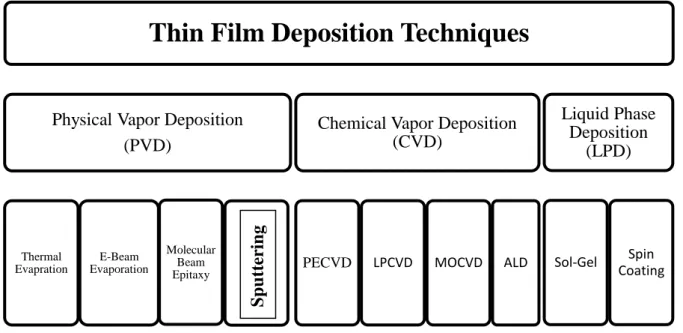
There is more than one classification for the thin films deposition techniques[25]. However, here we mention the most used classification. Thin film deposition techniques fall mainly under three categories, depending on the state of the materials deposited. The categories of such techniques are presented in the Fig. [1.1]. First one
4
is the Physical Vapor Deposition (PVD), where the material is ejected from a target and then transferred to the substrate through the vacuum. According to the type of target excitation that causes the ejection of the atoms, different systems are used. Under this category falls many systems, here are few of these deposition systems[25];
1- Thermal Evaporation, where the atoms are ejected by resistive heating, one of the draw backs is its limitation to low melting point metals. Also known as evaporative technique
2- Electron-beam Evaporation[26], as the name suggesting, in this system the atoms are ejected using an electron beam of high energy up to 30 KeV. It can evaporate any type of materials.
3- Molecular Beam Epitaxy (MBE)[27], it is known for its Knudsen effusion cells from which the element is slowly evaporated under a high vacuum of (10-11) torr. These three techniques are also known as the evaporative methods
4- Sputtering, where the material targets are bombarding by Argon ions to eject the atoms, as this work was conducted with this system, it will be discussed in details in chapter two. Another classification for this, is the Glow-Discharge process[25,28].
Second category is the Chemical Vapor Deposition (CVD), where the materials are in gas form as it under goes a series of decompositions and reactions before reaching the substrates. Such technique includes; Plasma Enhanced Chemical Vapor Deposition (PECVD), Low Pressure Chemical Vapor Deposition (LPCVD), Metal-Organic Chemical Vapor Deposition (MOCVD) and Atomic layer Deposition (ALD). The third category is the Liquid Phase Deposition (LPD), such as Sol-gel and Spin Coating. The most frequently used one for the doped zinc oxides thin films is the PVD. Each of the previously mentioned categories has its advantages over the others[29,30].
5
Thin Film Deposition Techniques
Physical Vapor Deposition (PVD) Thermal Evapration E-Beam Evaporation Molecular Beam Epitaxy
Chemical Vapor Deposition (CVD)
PECVD LPCVD MOCVD ALD
Liquid Phase Deposition
(LPD)
Sol-Gel Coating Spin
S p u tt er in g
6
1.3. Motivation
As mentioned earlier, ZnO is a candidate for the electronic applications, as it possesses a wide bandgap of 3.4 eV, however, it exhibits relatively high resistivity due to low carrier concentration and low carrier mobility, which led us to consider dopants material to tailor the thin film optical band gap as well as its conductivity. The effect of dopant materials such as aluminum (Al), indium (In) and gallium (Ga) were studied extensively through the last decade [31,32]. Among them, in particular (Ga) has shown to be less reactive and more resistant to oxidation compared to Al which makes them better dopant material [13]. Moreover, since Ga-O covalent bond length (1.92 Å) is almost similar to that of Zn-O covalent bond length (1.97 Å), Ga+3 can easily substitute Zn+2 without deteriorating the lattice[16,15,14]. On the other hand, In-Ga-ZnO doped films (IGZO) also possess excellent properties for their high carrier concentration and mobility at low cost along with high transparency and low temperature deposition processes.
Throughout the literature, two main draw backs were found, the lack of the mechanical characteristics studies for such materials and the effect of the deposition parameters on the metallic content percent in the thin films. Such draw backs were the motivation for this work. The XPS data has shown the atomic content of the metallic dopants inside the thin films as will be discussed in chapter 4 along with the mechanical characterizations of the sputtered doped zinc oxide thin films. Moreover, to investigate the effect of low substrate heating at 200 °C on the thin films characteristics and compare those to its counterpart Room Temperature (RT)-grown thin films, in terms of their characteristics and the possibility of using this low temperature for getting enhanced characteristics instead of the post-annealing process, in order to reduce the processes used.
7
1.4. Thesis Overview
This thesis work is composed of four chapters, where each is composed of subsections. Chapter one is the introduction where a brief intro about the functional oxide materials is presented along with the history of the thin films. Additionally, the motivation and the thesis overview are given. A detailed presentation for the experimental procedure carried in this study is demonstrated in addition to a simplified review about the main techniques and characterizations tool used in this study, is summarized in Chapter 2, where the operation principles of sputtering are pointed out along with the theory and calculations used in the interpretation of the characterization data obtained from each of the X-Ray Diffraction (XRD), Atomic Force Microscopy (AFM), X-Ray Photoelectron Spectroscopy (XPS), Ellipsometery, UV-Vis-Spectroscopy and the Nano-indentation for the mechanical characterization along with a detailed presentation for the experimental procedure carried in this study is demonstrated
The results and discussion are revealed in details in Chapter 3, where each group of the doped zinc oxide; IZO, GZO and IGZO, is expressed individually in a separate section, demonstrating the effect of the deposition parameters on the thin film characteristics. Only for GZO thin films, two groups are presented each for a different target used in the deposition. One is composed of (Ga2O3 / ZnO) 5/95 wt%
and the other target is composed of 7/93wt%. Moreover, in a separate section the mechanical characterization is demonstrated separately. In the end, the conclusion and the future prospective are suggested in Chapter 4.
8
Chapter 2
Experimental Methodology
Experimental Methodology
2.
The experimental part is mainly composed of two sections; the first is fabrication and film growth, where the deposition parameters and conditions are illustrated. The second is the film characterization, where the characterization tools and their data interpretation methods are explained. In this chapter a detailed description of the processes will be presented. Starting with substrate cleaning ending up with the characterization tools used. Each of IZO, GZO and IGZO, were deposited under these parameters [RF-power, (Ar) gas flow and pressure]. The main study was to develop a recipe that results in best film characteristics and then test this recipe with substrate heating at 200 ºC. Only for the GZO group, there were two targets used of different composition [5wt% and 7wt%] were used in an attempt to study the effect of the target composition on the characteristics of the deposited films especially the film composition.
9
2.1. Sputtering
Sputtering technique as mentioned earlier falls under many types of classifications. One of which is the PVD, as it represents the physical evaporation and deposition of the materials by using ion bombardment without any involvement of chemical reactions. Other known classification is Glow-Discharge process, where the glow-discharge is used to generate the energetic particles that strike the target causing atoms ejection. This happens in the presence of low-pressure gas that is usually argon (Ar)[33,34].
Sputtering technique itself has different systems within; such as Diode Sputtering and Magnetron sputtering. Each of these systems can be operated by both of direct current (DC) or radio frequency (RF)[28,35]. The simplest method used to be the DC-diode sputtering, where the glow discharge is guarded via dc voltage the cathode (metal target) and the anode (substrate) in the presence of Ar gas. Then the Ar+ ions generated in the glow discharge are accelerated resulting in the sputter of atoms from the target surface and in the deposition of these sputtered atoms in form of the thin films on the substrates. However, when it comes to insulator targets DC-diode sputtering isn’t the perfect choice, whereas the glow-discharge can’t be maintained any longer between the metal electrodes in the presence of insulator target. The diode sputtering was then introduced. The insulator target was supplied with RF-voltage to stabilize the glow-discharge during the process[33].
In magnetron sputtering[33], it’s the same where it can be operated via DC or RF, where either voltage is applied between the cathode (target) and the anode (substrate) in the presence sputtering gas usually (Ar). However, the idea in magnetron sputtering is to apply a magnetic field that is parallel to the cathode (target) in order entrap the electrons and confined them in a closed loop. The magnetic field applied results in the following sequential processes:
10
1- Increasing the collision rate between the electrons are the sputtering gas ions. 2- Increasing the plasma density.
3- Increases the current density at the target. 4- Increases the sputtering rate
This work was carried out by using the RF-Magnetron sputtering system. As it the most common used system for doped-ZnO thin films depositions, as within all these techniques – as mentioned in Introduction chapter – the RF- magnetron sputtering offers highly uniform and well-adhered thin films on large area substrates with high packing density even at low deposition temperatures.
2.1.1. Thin Films Deposition
Using VAKSIS NanoD-4S RF magnetron sputtering system, all of doped-ZnO thin films were deposited.
Silicon (Si) (100) and glass were used as substrates for all doped-ZnO thin films depositions. Substrates were first subjected to cleaning procedure, to make sure that substrates surfaces are ready for the thin film growth. Using acetone, isopropanol and deionized water (DI), the substrates were sonicated in each, for 5 minutes to get rid of any contamination before starting the deposition.
The distance between the substrate and the target was kept constant at 14 cm. the deposition was done with constant substrate rotation to keep the uniformity of the deposited thin films. In this study, high purity argon (Ar) gas was the only gas used as sputtering gas. The sputtering chamber was vacuumed to 1x10⁻⁶ Pa for starting a proper deposition. The targets were initially sputter cleaned for 5 minutes in (Ar) atmosphere before starting the deposition in order to remove any oxide layers that might have been formed upon previous depositions as well as removing any contaminations on the surface of the targets. The targets used were; IZO target bonded on copper back support, the target purity was 99% of (In2O3 / ZnO) 10/90
11
wt%, each of the two GZO targets were bonded on copper back support, with purity 99 % of (Ga2O3 / ZnO) 5/95 wt% and 7/93wt% and IGZO target of purity 99%
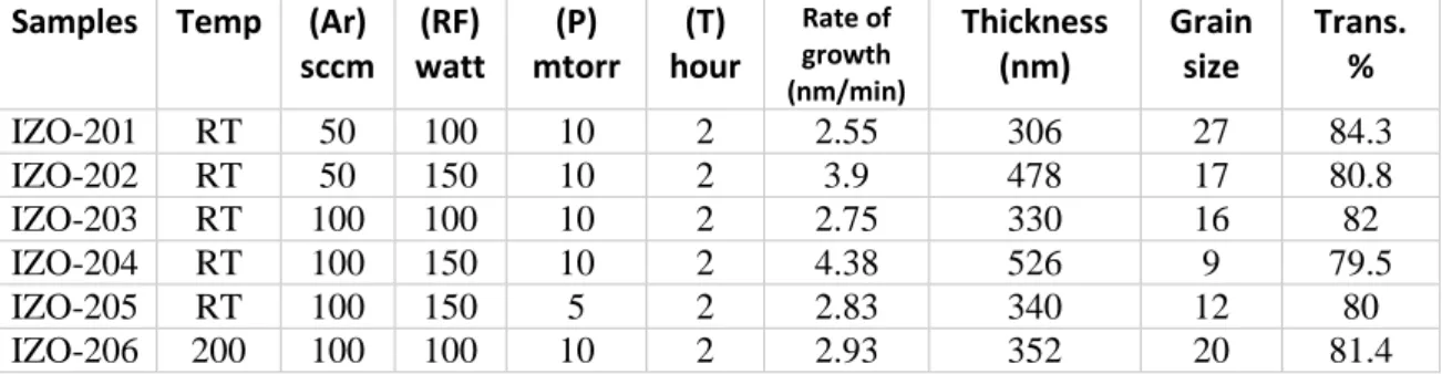
bonded on copper back support as well. Each of IZO, GZO and IGZO thin films depositions were performed in different (RF) plasma powers of 100 and 150 Watt, and different (Ar) flows of 50 and 100 sccm. The process pressure used was kept constant at 10 mtorr for IGZO thin films groups, while for IZO and GZO thin films were deposited at two different pressures of 5 and 10 mtorr. One of the recipes of each group was then subjected to substrate heating at 200 C. Table [2.1, 2.2, 2.3 and 2.4] show the recipes used for each group of the doped-ZnO thin films deposited. The deposition time was kept constant for 2 hours to determine the effect of the deposition parameters on the rate of deposition.
In order to perform the electrical characterization, metal contacts were deposited on the sides of the deposited thin films on the glass substrates. The metal contacts used were Tin (Sn) contacts. Four contacts were deposited on the edges of square shaped thin films deposited on the glass substrates.
A thicker film was grown for each of GZO and IGZO group, longer deposition time was used. Over 4 hours for GZO-5wt%, 7 hours for GZO-7wt% and 6 hours for IGZO. However, the continuous deposition for this long time interval surprisingly resulted in thick shaded films with transparency below 50%. This might be due to the high RF power used for deposition for long periods, which resulted in the formation of oxide layers over the surfaces of the target as well as the substrates. To overcome such results, a discontinuous deposition was performed for both GZO and IGZO, for intervals of 2 hours, resulted in thicker films around 900 nm. Meanwhile, the mechanical characterization was performed for the IZO thin films without the need for thicker film.
12 Table 2.1-1 IZO Deposition Parameters
Samples Temp (Ar)
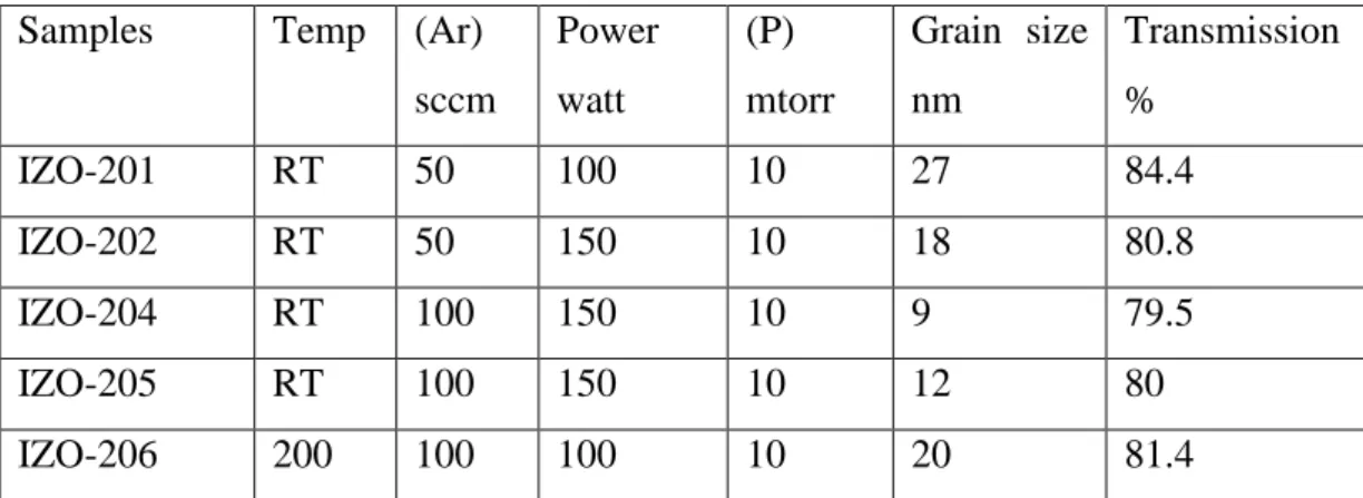
sccm (RF) watt (P) mtorr (T) hour Rate of growth (nm/min) Thickness (nm) Grain size Trans. % IZO-201 RT 50 100 10 2 2.55 306 27 84.3 IZO-202 RT 50 150 10 2 3.9 478 17 80.8 IZO-203 RT 100 100 10 2 2.75 330 16 82 IZO-204 RT 100 150 10 2 4.38 526 9 79.5 IZO-205 RT 100 150 5 2 2.83 340 12 80 IZO-206 200 100 100 10 2 2.93 352 20 81.4
Table 2.1-2 GZO-5wt%- Deposition Parameters
Samples Temp (Ar)
sccm (RF) watt (P) mtorr (T) hour Rate of growth (nm/min) Thickness (nm) Grain size (nm) Trans. % GZO-201 RT 50 100 5 2 2.11 254 15 87.1 GZO-202 RT 50 150 5 2 3.3 396 21 84.3 GZO-203 RT 50 150 10 2 1.75 210 10 70 GZO-205 RT 100 150 10 2 3 356 11 54.8 GZO-206 200 100 150 10 2 3.8 460 9 74.4
Table 2.1-3 GZO-7wt%-Deposition Parameters
Samples Temp (Ar)
sccm (RF) watt (P) mtorr (T) hour Rate of growth (nm/min) Thickness (nm) Grain size Trans. % GZO-301 RT 100 100 10 2 2.1 255 11 82.8 GZO-302 RT 100 150 10 2 2.4 290 7 88 GZO-304 200 100 100 10 2 2.2 260 10 84.8 GZO-305 200 100 150 10 2 2.6 315 7 86.7 GZO-306 200 50 100 10 2 2.2 270 9 88.8
Table 2.1-4 IGZO- Deposition Parameters
Samples Temp (Ar)
sccm (RF) watt (P) mtorr (T) hours Rate of growth (nm/min) Thickness (nm) Transmission % IGZO-201 RT 100 150 10 2 3 371 54 IGZO-202 RT 100 100 10 2 2.5 304 80 IGZO-204 RT 50 100 10 2 2.6 314 84.8 IGZO-205 200 50 100 10 2 2.58 310 86.6 IGZO-206 200 100 100 10 2 2.66 320 80.5
13
2.2. Thin Film Characterization Techniques
When it comes to the characterization, two questions are being asked; first what feature or characteristics do we need to study? Second, How to study this feature or characteristic? In general, Characterization of thin films is carried out to investigate their optical, electrical and mechanical properties along with their crystallinity, microstructure and chemical composition. All doped-ZnO thin films in this study were subjected to X-Ray Diffraction (XRD) to investigate their crystallinity and the estimate the grain size, Ellipsometery to determine their thicknesses and optical constants and to Carry 5000 System to determine their transmission. Whereas, selected thin films of each group of the doped-ZnO grown at RT and at 200 °C, were further subjected to each of X-ray photoelectron spectroscopy (XPS), hall measurement system, atomic force microscopy (AFM) and nano-indentation.
2.2.1. Optical and Electrical Characterization
The optical characterization was carried out by spectroscopic Ellipsometery and (UV–VIS–NIR) spectrophotometer. Spectroscopic Ellipsometery is an optical non-invasive characterization system that detects the change in polarization of the light after being reflected or transmitted from the thin films. The change of light polarization is represented by the amplitude ration (ψ) and phase difference (Δ). Since the light polarization is directly affected by both thicknesses and optical characteristics of the thin films, the reflected polarized light is detected and the data obtained is fitted through different models, giving in the exact thicknesses and optical constants of the thin films.
In this work, the thicknesses of the doped-ZnO thin films along with their optical constants were determined using angle spectroscopic Ellipsometery (V-VASE, J.A. Woollam) with rotating analyzer and xenon light source. Ellipsometery measurements were taken at multiple angles of incidence from 𝜃𝑎=70° to 75° in 5°
14
steps. The optical properties were modeled using the Cauchy model and Tauc– Lorentz dispersion formula for 𝑛(𝜆) and 𝑘(𝜆) [32], and a three-layer model including substrate, thin film, surface roughness, and ambient. Resulting in determining the film thicknesses and their optical constants, this in turn resulted in estimating the optical band gap. The optical constants are crucial for the optical band gap calculation. As to pin out the optical band gab, first, the absorption coefficient (α) should be calculated from the famous Beer’s Law:
𝜶 =
𝟒𝝅𝒌𝛌(2.1)
Where (α) is the absorption coefficient, (k) is the extinction coefficient and (λ) is the wavelength. By plotting (hνα)2 – Y axis- versus (hν) – X axis- the optical bandgap (Eg) is then estimated by extrapolating the linear behavior part of the plot to the
X-axis of the photon energy, as shown in Fig.[3.2.6]
Thin film on glass substrate was used for the transmission characterization. This Optical transmission was measured using an ultra violet–visible–near infrared (UV– VIS–NIR) single beam spectrophotometer (Ocean Optics HR4000CG-UV-NIR) in the wavelength range of [280-900] nm relative to air.
The electrical measurements were carried out by ezHEMS Hall Effect Measurement System, where the carrier mobility, film Resistivity and carrier concentration were measured, by using the Van der pauw method. Simply metallic contacts are made on the thin films edges on the glass substrate. The thin film sample is then attached to the four contact stage, which in turns introduced into the system’s chamber, where a current is then pass through the thin film in the presence of magnetic field. By knowing the thicknesses of the thin films, all of the resistivity (ρ), mobility (µ) and carrier concentration (η) are determined by the system.
15
2.2.2. X-ray Diffraction (XRD)
(XRD) is typically used to identify the crystalline nature of solid materials, as it identifies the degree or crystallinity, grain size, the crystal structure and orientation. Mainly an incident monochromatic X-ray is subjected to the samples, as the reflected rays have different path upon hitting different planes, a path difference is resulted. A constructive interference occurs only if this path difference is comparable to the atomic spacing, this is known as Bragg’s condition or Bragg’s Law:
𝟐𝒅 𝑺𝒊𝒏𝜽 = 𝒏𝝀 (2.2)
Where (n) is an integer, (λ) is the incident wave length, (d) spacing and (θ) is the diffraction angle.
Figure 2.2-1 Bragg’s diffraction
(https://commons.wikimedia.org/wiki/File:Bragg_diffraction.svg)
The doped-ZnO thin films crystallinity was determined via multi-purpose x-ray diffraction (XRD) in a PANalytical X'Pert PRO MRD diffractometer using Cu Kα (λ= 1.5406 Å) radiation, where the grain size was determined via the known scherrer’s equation as shown:
𝑫 =
𝜷 𝒄𝒐𝒔 𝜽𝟎.𝟗 𝝀 (2.3)16
Where D is the grain size, (λ=0.154 nm) is the x-ray wavelength, β is the FWHM in radians and θ is the Bragg’s diffraction angle.
2.2.3. X-ray photoelectron spectroscopy (XPS)
XPS is a quantitative spectroscopic and vacuum required technique that detects the elemental composition of the samples along with their chemical and bond states. It depends on measuring the kinetic energy of the electrons emitted from the samples upon irradiating them with known X-ray wavelength. Therefore the binding energy becomes a quantitative value that can be calculated from the following conservation of energy equation:
Eb = Ep – (Ek + ϕ) (2.4)
Where (Eb) is the binding energy of the electron, (Ep) is the photon energy of the
X-ray, (Ek) is the kinetic energy of the emitted electron and (ϕ) is the work function
which is a correction factor dependent on the instrument used. This technique detects both surface and bulk chemistry. In order to investigate the bulk, the sample undergoes etching using (Ar) ion beam.
The surface and bulk chemical compositions and bonding states of the doped-ZnO thin films RT-grown and their counterpart grown with substrate heating at 200°C , was determined by using X-ray photoelectron spectroscopy (XPS) using [Thermo Scientific K-Alpha spectrometer] with a mono-chromatized (Al Kα X-ray) source of (1486.6 eV). The samples were etched by (Ar) ion beam having an acceleration voltage of 1 kV for bulk investigation. The data of the fill scans and the elemental scan was fitted.
17
2.2.4. Atomic Force Microscopy and Nano-Indentation
The Surface morphology was examined for the chosen thin film using atomic force microscopes (AFM, Asylum Research MFP-3D) operating in the tapping mode using a triangular tip, where Surface roughness and grain size were estimated.
The mechanical characterization was then performed via Ambios Q-Scope AFM with nano-indentation modulus using Berkovich indenter method[36,37]. The measurement was done through one cycle of loading and unloading of a force by the nano-indenter tip, the (E) and the (H) of the deposited films were estimated from the data acquired in form of load versus displacement where the slop represents the contact stiffness (S). A schematic illustration of the indentation load is shown in Figure [2.2].
Figure 2.2-2 Schematic illustration of indentation load- displacement data [36]
The (H) was estimated from the following equation[36]:
𝐻 =
𝑃𝑚𝑎𝑥18
Where Pmax is the maximum load and A is the contact area, which in case of
Berkovich indenter the contact angel is 65.3º, which is represented as:
𝐴 = 24.5(hₑ)² (2.6)
Where, hₑ is the plastic depth of penetration. Another formula is used to estimate the elastic modulus: 𝟏 𝑬ₑ
=
(𝟏−𝝂𝟐) 𝑬+
(𝟏−𝝂𝒊𝟐) 𝑬𝒊 (2.7)Where (Ee) is the effective modulus, this effective modulus is the actual elastic
displacement that occurs in both the thin films and the indenter, each with its own elastic modulus and Poisson’s ratio; (E, ν) and (Ei, νi) for the sample and the
19
Chapter 3
Results and Discussion
Results and Discussion
3.
This chapter is composed of 4 sections, 3 of which are designated to a material group of doped-ZnO thin films characterization, while the fourth section is for the mechanical characterization. The structure of all the sections, is almost the same for the 3 groups [IZO, GZO and IGZO], the common structure is as follow; first, the effect of deposition parameters [RF-power, (Ar) flow and process pressure] on the crystallinity and the optical characteristics are being discussed in the beginning of each section of each material. Then a comparison is stated between the RT-grown thin films and the 200°C- grown thin films for each of; crystallinity and the optical characteristics, chemical composition, bond state and electrical properties, ending with morphological and mechanical properties.
20
3.1. Indium Zinc Oxide Thin Films (IZO)
The first material to be discussed in this study is the Indium doped Zinc Oxide Thin films (IZO). The IZO target that was used was bonded on copper back support, the target purity was 99% of (In2O3 / ZnO) 10/90 wt%. This group of thin films is
composed of 6 samples, 5 of which are grown in RT while 1 sample was grown at 200°C. The structure of the result starts with the effect of RF-power at two different values of (Ar) flows and vice versa at constant process pressure of 10 mtorr, then the effect of process pressure at constant RF-power and (Ar) flow of 100 watt and 100 sccm respectively. After which a comparison is stated between thin film grown at RT and that grown at 200°C, regarding their crystallinity and the optical characteristics, chemical composition, bond state and electrical properties, and finally their morphological and mechanical properties.
3.1.1. Crystallinity and Optical properties
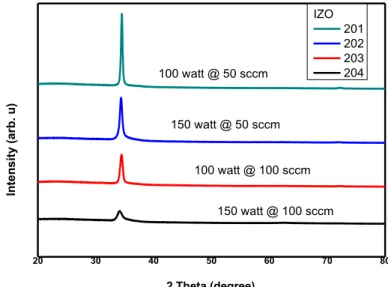
It’s known that the XRD patterns for sputtered ZnO thin films exhibits hexagonal wurtzite structure with c-axis orientation with dominant diffraction crystal peak of (002) at 35.4° [16,15,14,38]. And so apparently the doped ZnO thin films show the same characteristics. It’s worth mentioning that for the last decade the literature has shown that the IZO films grown at room temperature are amorphous[39–45], and the diffraction peaks would appear at higher growth temperatures starting at 400 °C or higher doping values of (In) [46]. However, in this study all the room temperature grown IZO thin films have shown the crystalline peak corresponding to the (002) plan, with different intensities as shown in Fig [3.1.1]. The (002) peak was the only dominant peak for all the grown IZO thin films, and no other peaks were observed.
21 20 30 40 50 60 70 80 IZO 201 202 203 204 100 watt @ 50 sccm 150 watt @ 50 sccm 100 watt @ 100 sccm 150 watt @ 100 sccm 2 Theta (degree) In te n si ty (a rb . u )
Figure 3.1-1 XRD Pattern of RT-grown thin films of IZO
All of the IZO thin films exhibit hexagonal wurtzite structure as expected. While keeping the process pressure constant at 10 mtorr, two values of RF-power were used (100 and 150 watt) once at 50 sccm of (Ar) flow and another at 100 sccm. It’s noticeable that higher RF-power decreases the intensity of the diffraction peak, along which the grain size decreases as well. The same observations were obtained while monitoring (Ar) flow, where the intensity of the diffraction peak decreased as well with increasing the (Ar) flow. It’s worth mentioning that there was no significant shift in the (002) peak angle, where the shift was only in order of 0.2° and 0.3° toward lower angle in case of increasing the RF- power at 50 sccm and 100 sccm (Ar) flow respectively. The calculated Grain Sizes are mentioned in Table [2.1]. This is came in contradiction with the GZO and IGZO results were the RF-power increment resulted in enhancement of the crystallinity of the thin films as it will be discussed later in this chapter in the GZO and IGZO thin film results section. In fig [3.1.2] the XRD pattern of two thin films RT-grown at different process pressure [10 and 5] mtorr.
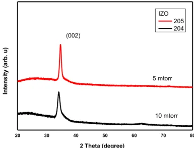
22 20 30 40 50 60 70 80 2 Theta (degree) In te n si ty (a rb . u ) IZO 205 204 (002) 10 mtorr 5 mtorr
Figure 3.1-2 XRD Pattern of IZO thin films at different process pressures
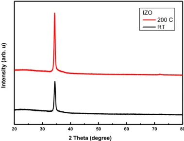
Decreasing the process pressure to 5 mtorr has increased the intensity of the dominant (002) peak when compared to the 10 mtorr-grown thin films. Moreover a shift toward higher diffraction angle by 0.7° was observed in case of decreasing the process pressure to 5 mtorr. The 200° C grown thin film (IZO-206) was deposited at 100 watt for RF-power, 100 sccm (Ar) flow and 10 mtorr process pressure which are the same deposition parameters as for sample (IZO-203) except for the growth temperature. Fig [3.1.3] shows the XRD patterns of IZO thin films grown under same parameters except for the temperature. The changes observed were first the intensity of the (002) peak increased, second the grain size increased from 16 nm to 20 nm representing RT-grown thin film and the 200 C grown thin film respectively.
23 20 30 40 50 60 70 80 2 Theta (degree) In te n si ty (a rb . u ) IZO 200 C RT
Figure 3.1-3 XRD patterns of IZO thin films grown at RT and 200 °C
For all the IZO thin films XRD patterns, no metallic peaks have been observed; neither for Zn or (In) indicating that (In) atoms is well incorporated into the thin films substituting the Zn atoms, and that the thin films are fully oxidized.
Ellipsometery measurements were taken at multiple angles of incidence from 𝜃𝑎=70° to 75° in 5° steps. The optical properties were modeled using the Cauchy model and Tauc–Lorentz dispersion formula for 𝑛(𝜆) and 𝑘(𝜆), and a three-layer model including substrate, film, surface roughness, and ambient. The results defined the film thicknesses and their optical constants; this in turn resulted in estimating the optical band gap. The thicknesses of the IZO thin films are shown in Table [2.1]. The rate of deposition hasn’t change much upon changing neither the process pressure nor the (Ar) gas flow, were it kept swinging from [2.5 to 2.9 nm/ min]. However, the rate of deposition has jumped to 3.9 nm/min and 4.3 nm/min upon using RF-power of 150 watt at 50 Sccm and 100 sccm (Ar) gas flow respectively, showing that the RF-power has a significant effect on the rate of growth, that might be due the increases of the ionization efficiency, which results in trapping more electron in the plasma in the vicinity of the substrate, resulting in higher deposition
24
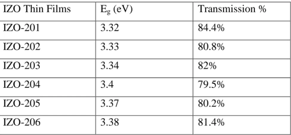
rate [34]. The (Eg) hasn’t change much compared to GZO, as will be discussed later,
where it kept swinging between 3.3 eV to 3.38 eV over the change of deposition parameters. Apparently, tailoring the band gap of ZnO thin films using (In) doping is not quite significantly. The optical bandgaps (Eg) are represented in table [3.1.1].
Table 3.1-1 Optical Bandgap and Transmission of IZO Thin Films
IZO Thin Films Eg (eV) Transmission %
IZO-201 3.32 84.4% IZO-202 3.33 80.8% IZO-203 3.34 82% IZO-204 3.4 79.5% IZO-205 3.37 80.2% IZO-206 3.38 81.4%
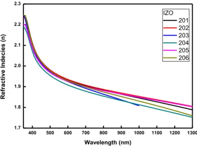
In fig [3.1.4] and fig. [3.1.5], the optical constants [(n) and (k)] are shown for all the IZO thin films. It can be seen that the refractive indices of all the IZO thin films are similar in the visible region except for the film grown under 200 °C, were its refractive index decreased. While in the infra-red region the refractive indices showed higher values for grown under 5 mtorr sccm, and the lower value for the thin film grown under 10 mtorr process pressure both thin films were grown under RF-power of 150 watt and 100 sccm (Ar) flow. The Extinction coefficient (k) were observed to be similar as well for all of the IZO thin films over the visible region, while it varies over the infra-red region.
25 400 500 600 700 800 900 1000 1100 1200 1300 1.7 1.8 1.9 2.0 2.1 2.2 2.3 R efr ac ti ve In d ec ie s (n ) Wavelength (nm) IZO 201 202 203 204 205 206
Figure 3.1-4 IZO thin films refractive indices
400 500 600 700 800 900 1000 1100 1200 1300 0.00 0.05 0.10 0.15 0.20 0.25 Ex ti n cti o n C o effi ci en t (k ) Wavelength (nm) IZO 201 202 203 204 205 206
26
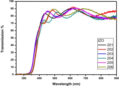
All the IZO thin films were highly transparent over the visible region recording transmission > 85%. Fig [3.1.6] represents the transmission spectra of the IZO thin films over the range of [280 – 900] nm. As seen there is only a small blue shift which agrees with the small changes over the optical band gap, extrapolated from the Ellipsometery data analysis. This blue shift according to Burestin-Moss repost, known as BM-Shift, is an indication for the increase of carrier concentration that is attributed with the increase of optical bandgap[43,47].
300 400 500 600 700 800 900 0 10 20 30 40 50 60 70 80 90 100 T ra n sm is si o n % Wavelength (nm) IZO 201 202 203 204 205 206
27
3.1.2. Chemical Composition, Bond State and Electrical
properties
Generally, X-Ray Photoelectron Spectroscopy was performed for the two thin films of each group of material. These two samples were deposited under same condition except for the temperature, where one is RT-grown while the other is grown at 200 °C. The two thin films have shown the following peaks; Ar 2p, C 1s, O 1s, Zn 2p and In 3p. The presence of the Ar 2p peak was an indication for a slight contamination within the XPS-chamber.
For O 1s, the peak positions are known to be classified typically into three main binding energy regions; low binding energy (BE) centered at 530.35 ± 0.3, medium BE at 531.31 ± 0.3 and high BE at 532.25 ± 0.3, each attributed to O-2 ions in the lattice, O-2 in the oxygen deficient regions and the chemosorbed oxygen on the surface either absorbed O2 or adsorbed H2O respectively[10,48,49]. After fitting the
data, the IZO thin films O1s peak was observed at lower (BE) and it was centered at 530.4 eV which is consistent with the O-2 ions within the lattice. There was no noticeable shift in the peaks for the thin film grown at 200 C. Moreover both films didn’t show any metallic peaks either for Zn or In, which indicate that both are on the oxide states, which in turns agrees with the XRD findings.
Thin films deposited on glass substrates were used for the electrical characterization via ezHEMS Hall system, where a four metal contacts were made on top of the thin films. Using van der pauw, a current was applied to the thin films in the presence of magnetic field, to determine the electrical characteristics of the IZO thin films. According to C. Lee et al. annealing at high temperatures >200 has a tendency to change the resistivity significantly, because the variation in resistivity due to the microstructural change, are based on thermally activated processes[43]. He has shown that amorphous IZO thin films sputtered by RF and annealed at 200 C acquired a low resistivity of 6.2 X 10⁻⁴ Ω.cm [39]. In this study, thin films grown at RT possess low resistivity, were the measurement recorded 5.97 X 10⁻⁴ Ω.cm, and
28
carrier concentration of 7.59 X 1020 cm-3 along with mobility of 2.75 V.cm.s. Here the results of RT-grown thin filsm were comparable to those annealed. As shown in [table 3.1.3] all the electrical characteristics of the IZO thin films are presented.
Table 3.1-2 Transmission of IZO Thin Films Samples Temp (Ar)
sccm Power watt (P) mtorr Grain size nm Transmission % IZO-201 RT 50 100 10 27 84.4 IZO-202 RT 50 150 10 18 80.8 IZO-204 RT 100 150 10 9 79.5 IZO-205 RT 100 150 10 12 80 IZO-206 200 100 100 10 20 81.4
Table 3.1-3 IZO thin films Electrical Properties Samples Thickness (nm) Resistivity (σ) (Ω.cm) Carrier Conc. (η) (cm-3) Mobility (µ) (cm2. V-1.S-1) IZO-201 306 4.15 x 10⁻³ 7.49 x 10¹⁹ 2.94 IZO-202 478 6.03 x 10⁻³ 1.09 x 10²⁰ 9.54 IZO-204 526 5.97 x 10⁻⁴ 7.59 x 10²⁰ 2.75 IZO-205 340 1.12 x 10⁻³ 7.89 x 10²⁰ 1 IZO-206 352 5.08 x 10⁻³ 5.54 x 10²⁰ 2.22
Apparently, the higher mobility was seen in thin film grown at 150 watt RF-power, 50 sccm (Ar) flow and process pressure of 10 mtorr, presented by thin film IZO-204. As shown the mobility increased from 2.94 to 9.54 cm2. V-1.S-1 when the RF-power increased from 100 watt to 150 watt; however it falls back to 2.75 upon increasing
29
the (Ar) flow up to 100 sccm as in thin film IZO-204. Moreover, the mobility deceases further when the process pressure dropped to 5 mtorr, where it possesses (1 cm2. V-1.S-1) which is very low compared to the records in literature which is reported in the range of (~5 to 10 cm2. V-1.S-1 ) [46]. We see here that the sensitivity decreased by an order of one magnitude to drop from 6.03 x 10⁻³ to 5.97 x 10⁻⁴ (Ω.cm). As shown, this decrease in resistivity was on the expenses of the mobility which dropped apparently from (~10 to ~ 2 m2. V-1.S-1).
3.1.3. Morphological Structure
2D AFM images of IZO thin films of 1µm x 1µm are shown in fig [3.1.7], for both grown at RT and at 200 C. its known that amorphous IZO thin films acquire low RMS > 1 nm[41,50]. The thin films showed that they exhibit high surface roughness; this might be because the thin films exhibit poly-crystalline rather than amorphous characteristics as it was indicated from the XRD. It appears that the thin film deposited at low (Ar) flow of 50 sccm has shown RMS of 4.22 nm. And as the (Ar) flow increased up to 100 sccm, the RMS was increased up to 5.37 nm. Moreover the RMS also increased significantly upon increasing the RF-power to 150 watt, resulting in RMS of 6.96 nm. The thin film grown at 200 °C showed roughhouses of 3.88 nm, which is lower than those of the RT-grown thin films, however, thin film deposited at RT but at low process pressure of 5 mtorr instead of 10 mtorr, has shown the lowest RMS among the rest of the IZO thin films, giving RMS of 1.66. This is an indication process pressure has a major effect on the roughness of IZO thin films and that they can be tailored upon the desired application as the case of organic light emitting diodes (OLED), that requires transparent thin films of low surface roughness, which is found to be a critical aspect for the OLED life time performance[50] and in terms of flexibility[51].
30
a) b)
31
3.2. Gallium Zinc Oxide Thin Films (GZO)
The second material of this study was GZO, where two targets each bonded on copper back support, with purity 99 % of (Ga2O3 / ZnO) 5/95 wt% and 7/93wt%,
were used for the thin films depositions. The structure of this section is the same as previous, as a starting point, the optical properties and crystallinity of the films are demonstrated followed by, the film composition and bond state, morphology and electrical properties. Each of these characteristics is discussed with respect to the parameter involved in their deposition. Since this section is for two groups of different target compositions, the thin film groups are assigned as GZO-5wt% and GZO-7wt% to differentiate between the two groups.
3.2.1. Crystallinity and Optical properties
It’s known that the XRD patterns for sputtered ZnO thin films exhibits hexagonal wurtzite structure with c-axis orientation with dominant diffraction crystal peak of (002) at 35.4°[16,15,14,38]. Starting with GZO-5wt%, XRD pattern for the GZO thin films deposited at different parameters are presented in figures [3.2.1, 3.2.2 and 3.2.3] for different RF powers, different pressure and different Ar flow respectively. All of the GZO thin films exhibit hexagonal wurtzite structure as expected. However, three peaks of (100), (002), and (101) have appeared with different intensities in most of the samples indicating that the thin films of GZO-5wt% acquire polycrystalline hexagonal wurtzite structure and the variation in the diffraction lines of the three peaks indicate that the thin films acquire asymmetry crystallite [16]. (002) peak was dominant only in case of the deposited thin film at pressure of 5 motrr.
As shown in Fig [3.2.1] two main features are observed upon increasing the RF-Power, first is that the (002) peak shifted toward the left to lower diffraction angle from 34.4° to 33.2°, second is that the intensity of the (002) peak is significantly increased. This indicates that the film crystalline features have enhanced with the RF-power increment, however the shift to the lower diffraction angle is suggested to
32
be due to the increase in the inter-planer spacing[38]. The grain size was calculated using scherrer’s equation, giving 15.5 nm for the sample deposited at 100 watt and 21.6 nm for the thin film deposited at 150 watt, which shows that as the power increase the grain size increases as well. In figure [3.2.2] where the films deposited at different pressures of 5 mtorr and 10 mtorr are shown, the features observed are that the film shifted to higher angle with increasing the pressure from 33.2° to 34.2°. Moreover, two other diffraction peaks (100) and (101) were observed, indicating that the crystallinity and epitaxiallity of the thin film is decreasing as the pressure increasing [14].
Although that the presence of these additional diffraction peak indicates less crystalline and less epitaxial thin film, the grain size was significantly decreased from 21 nm to 10 nm. The same three peaks of (100), (002) and (101) were observed for the films deposited at different (Ar) gas flow of 50 and 100 sccm. The grain size was slightly differed from the 50 sccm to 100 sccm by 1 nm, where the film deposited at 50 sccm acquired grain size of 10.2 nm while the film deposited at 100 sccm acquired grain size of 11.4 nm. It’s clear that for GZO-5wt% group two contradictory observations have been shown upon increasing RF-power and increasing the pressure, where the diffraction peak (002) which was the dominant peak only in case of the high power, has shifted to the lower angle in case of the higher RF-power while for higher pressure the diffraction peak shifted to higher angle. For grain size, it was observed that it increases as the RF-Power increasing while decreases as the pressure increases.
All these observation indicate that the crystallinity in enhanced with high RF-power and low pressure. While the difference in the (Ar) used didn’t have any significant effect on either the crystallinity or the grain size. For the thicker sample of 900 nm deposited for the mechanical characteristics, many other diffraction peaks have slightly appeared as shown in fig [3.2.4], indicating the loss of epitaxiallity along with the crystallinity of the films at higher thickness. This might be a result of the discontinuous time interval of deposition.
33 20 30 40 50 60 70 80 In te n si ty ( A rb .u ) 2 Theta (degree) GZO 150 Watt 100 watt
Figure 3.2-1 XRD Pattern of GZO thin films Deposited at different RF powers
20 30 40 50 60 70 80 In te n si ty ( A rb .u ) 2 Theta (degree) GZO 5 mtorr 10 mtorr
34 20 30 40 50 60 70 80 In te n si ty ( A rb .u ) 2 Theta (degree) GZO 100 sccm 50 sccm
Figure 3.2-3 XRD Pattern of GZO thin films Deposited at different (Ar) flows
20 30 40 50 60 70 80 In te n si ty ( A rb .u ) 2 Theta (degree) 912 nm 460 nm (101) 35.7 35.9 (002) 33.6 33.9 (100) 31.6 31.7 (102) 46.8 (110) 55.9 (103) 61.8 (112) 68
35
Regarding the GZO-7wt% thin film group, as mentioned earlier also exhibits hexagonal wurtzite structure with c-axis orientation with dominant diffraction crystal peak of (002) with no additional diffraction peaks observed. In all GZO-7wt% thin films, one dominant peak appeared at (002) with no additional peaks, however the intensity of this peak changes upon the change in the deposition parameters. The effect of RF power is shown in fig [3.2.5] that represents the XRD pattern of GZO-7wt% thin films deposited at 100 watt and 150 watt. The intensity of the diffraction peak decreased with the higher deposition power that results in an increase in the FWHM values, which in turn decreased the grain size from 11 nm to 7 nm; moreover there was a slight shift to the left in the diffraction peak towards lower angle with the higher RF-power. Since 100 watt sample showed relatively better crystallinity, the recipe was tested directly with substrate heating at 200 °C.
20 30 40 50 60 70 80 In te n is ty ( ar b .u ) 2 Theta (degree) GZO-7wt% 150 watt 100 watt (002) 33.8 (002) 34.1
Figure 3.2-5 XRD Pattern of GZO-7wt% thin films deposited at 100 and 150 watt
![Figure 2.2-2 Schematic illustration of indentation load- displacement data [36]](https://thumb-eu.123doks.com/thumbv2/9libnet/5997909.126148/32.892.375.551.627.922/figure-schematic-illustration-indentation-load-displacement-data.webp)