Y = Mo, Cr, W; and M = Li, Na兲 nanowires and bulk phase of M2Y6X6. We found that not only Mo6X6, but also transition metal and chalcogen atoms lying in the same columns of Mo and Se can form stable nanowires consisting of staggered triangles of Y3X3. We have shown that all wires have nonmagnetic ground states in their equilibrium geometry. Furthermore, these structures can be either a metal or semiconductor depending on the type of chalcogen element. All Y6X6wires with X = Te atom are semiconductors. Mechanical stability, elastic stiffness constants, breaking point, and breaking force of these wires have been calculated in order to inves-tigate the strength of these wires. Ab initio molecular dynamic simulations performed at 500 K suggest that overall structure remains unchanged at high temperature. Adsorption of H, O, and transition metal atoms like Cr and Ti on Mo6Se6have been investigated for possible functionalization. All these elements interact with Mo6Se6wire forming strong chemisorption bonds, and a permanent magnetic moment is induced upon the adsorption of Cr or Ti atoms. Molybdenum selenide-type nanowires can be alternative for carbon nanotubes, since the crystalline ropes consisting of one type of共M2兲Y6X6structures can be decomposed into individual nanowires by using solvents, and an individual nanowire by itself is either a metal or semiconductor and can be functionalized.
DOI:10.1103/PhysRevB.74.235433 PACS number共s兲: 73.63.Nm, 73.22.⫺f, 75.75.⫹a
I. INTRODUCTION
In spite of active research carried out on the mechanical, electronic, and transport properties of nanowires for several decades,1–3 fabricating interconnects which fit molecular
electronic devices have remained one of the major challenges in nanotechnology. Recently, carbon nanotubes4have been a
focus of attention because of their diameter in nanometer scale and uniform cylindrical shape allowing ballistic transport.5–7These tubes can be metallic or semiconducting
depending on the diameter and chirality angle. They are strong along the axial direction, but flexible radially. More-over, they can be coated with metal atoms.8–10 Nowadays,
carbon nanotubes are synthesized in bundles which consist of a large number of tubes of different radius and chiral angle. It seems impossible to fabricate carbon nanotubes in desired diameter and chiral angle or select them from bundles. This difficulty remains a serious obstacle facing the wide range of possible technological applications of carbon nanotubes.
Molybdenum based nanowires with stoichiometry
M2Y6X6 共where M =Li,Na, Y =Mo, and X=Se,Te,S兲 have
been synthesized by Potel11and Tarascon.12These materials
grow also in ropes of structurally and electronically identical nanowires. Each rope has crystalline structure in a hexagonal close packed form. A weak interaction holds the wires to-gether. The isolated wires are easily obtained from the bundles by using a highly polar solvent.13 Although these
materials are in bulk crystalline form, they show one-dimensional 共1D兲 properties due to the existence of long
Y6X6 atomic chains. Chew et al.14 have used the nuclear
magnetic-resonance spectroscopy to probe the electronic
structure of the M cation sites in M2Mo6Se6, M
=共Li,Rb,Cs,In兲. Tarascon et al.12have reported that charge
transport properties of M2Mo6X6 共M =K,Rb,Cs,Tl and X
= Se, Te兲 nanowires can vary from metallic to semiconduct-ing, depending on the temperature and composition. Re-cently, Venkataraman et al.15,16have synthesized and charac-terized the structure and electronic properties of the bulk phase of Li2Mo6Se6 and isolated Mo6Se6 chains. Their
ob-servations have confirmed the 1D nature of these materials. Local density of states共LDOS兲 is consistent with Van Hove singularities peculiar to 1D systems. They have also ob-served that Peierls transition does not occur at least down to 5 K. Venkataraman et al.16 have observed Luttinger liquid
behavior in Mo6Se6 nanowires, where linear conductance
and current exhibit a power law dependence on temperature and bias voltage, respectively. Exponent governing of these power laws decreases with increasing number of conducting channels. Mechanical and electronic properties of Li2Mo6Se6
and individual Mo6Se6 nanowires have been studied by Riberio et al.17 Electronic structure of Li
2Mo6Se6, isolated
Mo6Se6wires, and bulk Li2Mo6Se6are similar. Lithium atom
behaves as a donor atom. Adsorption of Li does not modify the overall picture of the band structure, since the alkali atom, having very low ionization potential, easily donates its valence electron to the conduction band. Vilfan18,19has stud-ied electronic and elastic properties of bare and Li doped Mo6S6 nanowires with ab initio calculations. Mo6S6 wires
also weakly interact in bulk form like Mo6Se6. The elastic
constant of these wires along the wire axis is 320 Gpa which is higher than steel but smaller than the single wall carbon nanotubes 共SWNT兲.20,21 Recently, Mo
6S9−xIx wires have been synthesized.22The structure of these wires consists of a
rigid Mo octahedra. Each Mo atom is decorated with S or I atoms and octahedras are again connected by three S or I atoms. Yet, exact structure of these wires is unknown. Yang
et al.23 have theoretically studied equilibrium geometry and
electronic structure of Mo6S9I9nanowires. Different isomers
of these wires exhibit different electrical and magnetic prop-erties. They can become either conductors or narrow gap magnetic semiconductors. Moreover, thin films of metallic Li2Mo6Se6nanowire ropes can be used as a chemical sensor.
Xiubin et al.24,25have showed that resistance of such a thin
film changes upon adsorption of organic molecules, suggest-ing that the electrical conductance of the Mo6Se6 nanowire
may change with the type and number of adsorbed atoms or molecules.
Because of their synthesis as structurally identical wires with useful electronic and mechanical properties, Mo6Se6-type nanowires can be a potential alternative to
car-bon nanotubes. In this respect, we believe that Y6X6-type
nanowires will be a subject of interest in the future. This work presents a systematic investigation of structural, me-chanical, and electronic properties of M2Y6X6, Y6X6 共X
= Se, Te, S; Y = Mo, Cr, W; and M = Li, Na兲 type nanowires and bulk phase of M2Y6X6, within the density functional
theory. Our results are important for further research on these nanowires to reveal their properties for practical technologi-cal applications.
II. DESCRIPTION OF THE METHOD
We have performed first-principles plane-wave calculations26,27within density functional theory共DFT兲28 us-ing ultrasoft pseudopotentials.29 The exchange correlation
potential has been approximated by generalized gradient ap-proximation共GGA兲.30For partial occupancies, we have used
the Methfessel-Paxton smearing method.31 The width of
smearing has been chosen as 0.1 eV for atomic relaxation and 0.01 eV for accurate energy band and electronic density of states calculations. All structures have been treated by supercell geometry共with lattice parameters asc, bsc, and csc兲 using periodic boundary conditions. To prevent interaction between adjacent isolated wires, a large spacing 共asc= bsc ⬃15 Å兲 has been taken. For single wire calculations, csc corresponds to the lattice constant c0 共c0 being the lattice
constant of the Y6X6along the wire axis or z direction兲, but csc= 2c0 for double cell. Convergence with respect to the
number of plane waves used in expanding Bloch functions and k points in sampling the Brillouin zone have been tested for each wire system. In the self-consistent potential and to-tal energy calculations, the Brillouin zone of nanowires has been sampled by共1⫻1⫻15兲 and 共1⫻1⫻9兲 mesh points in the k space within the Monkhorst-Pack scheme32 for single and double cells, respectively, since there is no dispersion in
x and y directions. For bulk calculations, we have used a grid
of共3⫻3⫻15兲 k points. A plane-wave basis set with kinetic energy cutoff ប2兩k+G兩2/ 2m艋300 eV has been used. All
atomic positions and lattice parameters have been optimized by using the conjugate gradient method where total energy and atomic forces are minimized. The convergence for en-ergy has been chosen as 10−5eV between two ionic steps,
and the maximum force allowed on each atom is 0.05 eV/ Å.
III. STRUCTURE
The overall atomic structure of Mo6Se6-type nanowires
and their bulk crystalline are described in Fig. 1. The unit cell of an isolated nanowire consists of two staggered trian-gular layers composed of Y3X3 units. Each layer consists of
an equilateral triangle having one chalcogen atom at each corner and one metal atom placed between each chalcogen pair. Bulk structure unit cell has hexagonal symmetry, where nanowires along the z direction are arranged to form hexa-gons. Alkali atoms 共Li or Na兲 are placed between atomic planes as illustrated in Fig.1共c兲.
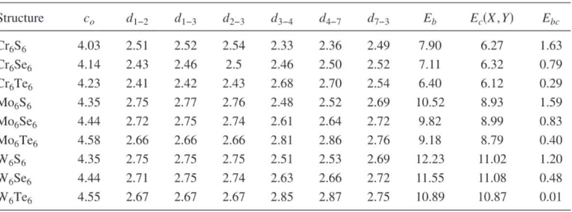
We first study the equilibrium structural properties of iso-lated nanowires and bulk structures by using total energy calculations where the atomic structure is fully optimized. Our detailed analysis reveals that the geometric structure in Fig. 1 is not unique to the experimentally synthesized Mo6Se6compound, but other metal and chalcogen atoms of the same columns can also form such structures. The binding energy Eb and the lattice constant c0 of optimized structure
of Y6X6nanowires are given in TableI. The lattice constants
we have calculated for Mo6Se6, Mo6S6, and bulk Li2Mo6Se6
are consistent with those reported in earlier experimental and theoretical works. Experimental value of c0 for isolated
Mo6Se6 is 4.5± 0.1 Å.15 Vilfan18 has calculated lattice con-FIG. 1.共Color online兲 共a兲 Side and 共b兲 top view of the atomic structure of isolated wires Y6X6. Y = Mo, Cr, W; and X = S, Se, Te. The metal and chalcogen atoms labeled as共1, 2, 3兲 and 共4, 5, 6兲, respectively, are on the same plane. Relevant interatomic distances d1–2, d1–3, d2–3,
d3–4, d4–7, and d7–3are between the atoms共1–2兲, 共1–3兲, 共2–3兲, 共3–4兲, 共4–7兲, and 共7–3兲, respectively. 共c兲 The unit cell of bulk 共periodic兲 structure of M2Y6X6where M = Li or Na are in different planes.
stant and in-plane Mo-Mo, Mo-S, and interplane Mo-Mo and Mo-S distances of an isolated Mo6S6 wire as 4.35± 0.05,
2.74, 2.49, 2.69, and 2.62 Å, respectively. These structural parameters are in agreement with our calculated structure parameters for Mo6S6. Eb per formula unit 共f.u兲 of isolated wire is calculated as
Eb=共6Ea关X兴 + 6Ea关Y兴 − ET关Y6X6兴兲/6, 共1兲
where Ea关X兴 and Ea关Y兴 are the ground state energies of single chalcogen and metal atoms, respectively, and
ET关Y6X6兴 is the optimized total energy of a nonmagnetic
nanowire. High Eb obtained for each nanowire can provide some clues about stability of the system. Furthermore, we compare Ebof Y6X6wires with Ec共X,Y兲, which is defined as the sum of bulk cohesive energies of each element forming the Y6X6 wire. Accordingly, Ec关X,Y兴=Ec关X兴+Ec关Y兴, where
Ec关X兴 and Ec关Y兴 are the calculated cohesive energy per atom of X and Y bulk crystals, respectively.33,34 Binding energies
of Y6X6 nanowires per f.u. with respect to the cohesive
en-ergy of metal and chalcogen crystals are calculated as
Ebc= Eb− Ec共X,Y兲. 共2兲 Calculated Ebc and Ec共X,Y兲 are presented in TableI. Ebcof
Y6X6nanowires ranges from 0.01 eV to 1.63 eV, and hence
the formation of them from bulk is exothermic. These results indicate that Y6X6nanowires can be produced from bulk
pre-cursors.
It is interesting to note that Ebincreases as the row num-ber of metal atom increases. On the other hand, in each metal group, Eb decreases with increasing row number of chalco-gen atom since transition metal共TM兲 atoms are located be-tween two chalcogen atoms occupying the corners of the large triangle, larger radius of metal but smaller radius of chalcogen enhances the binding energy. The variation in Eb 共and also Ebc兲 shows the similar trend in the variation of cohesive energies of these elements in bulk phase共see Fig. 2兲.35For the bulk structure, the optimized lattice parameters
are a = 8.52 and c0= 4.5 Å for Li2Mo6Se6. These values are
consistent with the experimental values11,16 of a = 8.5 and
c0= 4.48 Å. Lattice parameter coof isolated wire changes by 1.4% in the bulk crystal. The amounts of change in the
in-teratomic distances of Mo6Se6nanowire are also small upon
formation of crystal. It is noted that the variation of the lat-tice constant of the nanowires follows the same trend of the bulk crystal structure parameters of the corresponding metal atoms 共Y兲. The nature of interaction holding Li2Mo6Se6 in bulk phase is conjectured to be attractive van der Waals teraction. In principles, DFT includes the van der Waals in-teraction. However, it is poorly represented in GGA, but relatively better represented in LDA. In addition to GGA calculations which predicted co and a of Li2Mo6Se6 crystal
in good agreement with experimental data, we have also car-ried out LDA calculations using Ceperley-Alder exchange-correlation potential.36 LDA results underestimate c
o and a. On the other hand, the smallest Se-Se, Se-Li, and Mo-Se interatomic distances between adjoint wires in bulk phase are
Mo6Se6 4.44 2.72 2.75 2.74 2.61 2.64 2.72 9.82 8.99 0.83
Mo6Te6 4.58 2.66 2.66 2.66 2.81 2.86 2.76 9.18 8.79 0.40
W6S6 4.35 2.75 2.75 2.75 2.51 2.53 2.69 12.23 11.02 1.20
W6Se6 4.44 2.71 2.75 2.74 2.63 2.66 2.72 11.55 11.08 0.48
W6Te6 4.55 2.67 2.67 2.67 2.85 2.87 2.75 10.89 10.87 0.01
FIG. 2. 共Color online兲Variation of binding energy Ebof Y6X6 nanowires with respect to different X and Y atoms. Insets show the bulk cohesive energy of X or Y bulk crystals.
found to be larger than the corresponding sum of atomic radii. In addition to these arguments, the calculated binding energy of Li2Mo6Se6 crystal relative to the energy of
Li2Mo6Se6nanowires is only 0.9 eV. Based on these results,
we conclude that nanowires in the bulk crystal are held to-gether mainly by moderate chemical interaction.
As a next step, we have carried out finite temperature ab
initio MD calculations for one type of nanowires in each
metal group, namely Cr6Se6, Mo6Te6, and W6S6. We have
performed calculations in double cells at 500 K for 250 time steps共0.5 ps兲 using a Langevin thermostat. We also carried out ab initio MD calculations in six unit cells共as a periodi-cally repeating cell兲 at 500 K for 1 ps using a microcanoni-cal ensemble but by smicrocanoni-caling velocities at each time step. The Brillouin zone has been represented by a single k point at⌫. These ab initio MD calculations indicate that these wires are stable at high temperature. Trajectories of each atom in the course of MD simulations are illustrated around their equi-librium positions in Fig.3. Maximum displacements of at-oms from their equilibrium positions are highest共lowest兲 in Cr6Se6 共W6S6兲. Due to constraints of atomic motion at the
corner of the inner triangle, deviation of chalcogen atoms from equilibrim are higher than metal atoms.
IV. ELECTRONIC PROPERTIES
The detailed form of band structure around the Fermi en-ergy共EF兲 determines the electronic properties of these
mate-rials. The number of bands which cross EFis crucial for the quantum ballistic conductance and the stability of nanowire. Under ideal conditions and within Landauer theory, the equi-librium conductance of an infinite wire would be determined by the number of bands 共n兲 crossing the EF, namely G = 2ne2/ h. However, in a recent study on Mo6Se6 nanowires,
Luttinger liquid behavior has been observed16
experimen-tally. This suggests that conductance of Mo6Se6 nanowires
may not be written in a simple Landauer form. Due to electron-electron interaction in 1D geometry, equilibrium conductance of defect-free infinite Mo6Se6wire can be
writ-ten as G = 2nKe2/ h, where K represents the dimensionless
electron-electron interaction parameter of Luttinger liquid. Our analysis indicates that the form of the energy band structure that belongs to each metal group is similar. In Fig. 4, only the band structure of isolated wires with Y = Cr are illustrated as prototypes. For X = S and Se cases, the isolated wires are metallic with three bands crossing EF. Our partial density of states共PDOS兲 analysis presented in Fig.4共e兲–4共g兲
FIG. 3.共Color online兲 Trajectories of atoms around equilibrium position for one unit cell in共a兲 Cr6Se6,共b兲 Mo6Te6, and共c兲 W6S6. Atoms in upper plane共lower兲 are labeled by orange 共red兲 color.
FIG. 4. 共Color online兲 The band structure and partial density of states共PDOS兲 of Cr6S6共a兲, 共e兲; Cr6Se6共b兲, 共f兲; Cr6Te6共c兲, 共g兲; and band structure of bulk Li2Cr6Te6 共d兲. Fermi level of metallic sys-tems shown by dashed lines marks the zero of energy. In semicon-ducting Cr6Te6, the zero of the energy indicates the top of the valence band. To resolve the band gap in共g兲 the smearing of states is decreased. In contrast, the singularities of density of states disap-peared owing to the smearing of states by the Gaussian function in 共e兲 and 共f兲.
For example, while the Cr atom gives 0.17 e and 0.05 e to S and Se, respectively, it takes 0.28 e from the Te atom. The trend is similar for other TM atoms共Mo, W兲. Due to charge transfer to the Cr atom from Te, the electronic potential at Cr atom rises in energy. The energy gaps are 0.39, 0.23, and 0.25 eV for Cr6Te6, Mo6Te6, and W6Te6, respectively. Fig-ure 4共d兲 shows the band structure of bulk Li2Cr6Te6 along
the⌫-A 共along the wire兲 and A-L directions 共perpendicular to the wire兲. In bulk systems, conduction electrons are localized on wires. The dispersion of bands along the⌫-A direction is stronger than the dispersion of bands along the A-L direction. This situation is consistent with the 1D nature of bulk
M2Y6X6compounds. In this respect, our findings confirm the
experimental results and other theoretical works. Very small band dispersions along a direction perpendicular to the wire indicate that the interaction between the individual chains is very weak. In the bulk case, alkali atoms 共Li, Na兲 donate their electrons to wires and change the number of bands crossing the EF. This charge transfer raises the EF and re-duces the number of conduction bands of wires. For this reason, unlike Cr6Te6nanowire, bulk Li2Cr6Te6has metallic behavior.
V. MECHANICAL PROPERTIES
Our results concerning the stability and mechanical prop-erties of the nanowires provide valuable information for the synthesis of these materials in the future. First, we present our extensive analysis of mechanical stability.
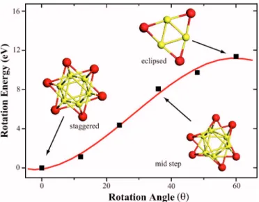
A. Rotation from staggered to eclipsed geometry
First, we have analyzed the stability of wires with respect to the rotation of the staggered triangular planes formed by
Y3X3. In this study, one of the planes in the unit cell is fixed
and the adjacent one is rotated in 12° steps. At each step, only the lattice constant csc= c is optimized. In Fig. 5, we
show the variation of rotation energy, i.e. ET共兲−ET共= 0兲 as a function of rotation angle. Here, ET共兲 denotes the total energy of a wire at a given rotation angle . Calculations indicate that there is a high energy barrier⌬Q 关=ET共= 60兲 − ET共= 0兲兴 between eclipsed and staggered structures. All wires prefer the staggered geometry and they relax from the eclipsed to the staggered geometry without any barrier. Inter-estingly, all isolated wires are nonmagnetic for all.
B. Elastic stiffness
The axial strength of these wires has been investigated by calculating the elastic stiffness constant , which is defined as the second derivative of the strain energy per unit cell with respect to the axial strain ⑀zz, namely = d2ET/ d⑀zz
2
. While calculating , we apply a small deformation to the wire along the wire axis in order to stay in the harmonic region. Consequently, we can use the Hooke’s law to find restoring force. The calculatedvalues are listed in TableII. Most of them are higher than that of steel and also compa-rable with the theoretically predicted value for the 共8,0兲 single wall Si nanotube 共23 eV/atom兲.37 However, they are
smaller than that of the single wall carbon nanotube as well as the linear carbon chain which are calculated to be
FIG. 5. 共Color online兲 Variation of the total energy ET共兲 of Mo6Se6 wire with the rotation angle between the adjacent tri-angles. The continuing line is fit to calculated data. The equilibrium total energy ET共=0兲 is set to zero.
TABLE II. First row: Elastic stiffness constants. Second row: Minimum strainzz,Breqiured to break the isolated Y6X6wire. Third row: Breaking-strain energy EB 共or strain energy required until zz,B兲 per cell.
Fourth row: Ratio of strain energy tozz,B共EB/zz,B兲.
Cr6S6 Cr6Se6 Cr6Te6 Mo6S6 Mo6Se6 Mo6Te6 W6S6 W6Se6 W6Te6
共eV/cell兲 192 117 156 280 254 210 306 254 220
zz,B共%兲 9.3 8.2 10.8 6.9 8.2 9.1 6.5 8.0 10.0
EB共eV per cell兲 1.15 1.02 1.50 1.17 1.29 1.44 1.29 1.49 1.73
52– 60 eV/atom38 and 119 eV/atom,39 respectively. In each
metal group, the wire with a S atom is stiffer than others and the stiffness decreases from S to Te in the Mo and W group. This trend is not followed in the Cr case. In each chalcogen group,tends to decrease from W to Cr. These results indi-cate thatis related to the radii of atoms. Highest 共lowest兲 value is obtained for largest共smallest兲 radius of a metal atom and smallest共largest兲 radius of a chalcogen atom.
C. Breaking strain
The variation of the total energy versuszz has been cal-culated for all wires by increasing c0 uniformly in small
steps. At each step, the structure has been fully relaxed. In Fig.6, we illustrate our results for Cr6Se6. In the same figure,
we also show the tensile force共minus the restoring force, i.e.
FT=
1
c0ET/zz兲. Here, one distinguishes two different be-haviors. In the first one, the wires elongate uniformly under axial tensile force by conserving symmetry. Beyond a critical strain or maximum critical force Fc, a smaller force is re-quired to achieve further elongation. This point coincides with the inflection point of the energy ET共zz兲 curve in Fig.6. This is taken usually as the breaking point of the atomic
chains. Passing through the breaking point the wire expands uniformly but with a tensile force FTsmaller than Fc.
In Y6X6wires, we deduce also a behavior which is
differ-ent from uniform elongation. Before one reaches the inflec-tion point at a certain value ofzz, a structural transformation starts where bonds between TM atoms in different planes break, and concomitantly chalcogen atoms find a place be-tween them. This structural transformation is derived by the elastic energy stored in the wire and is an anharmonic symmetry-breaking process. The system becomes more en-ergetic by lowering the total energy ET whereby the wire expands irregularly. We notice that a similar anharmonic structural transformation after an elastic deformation took place in the stretching of metal nanowires with finite cross section.40The transformation may release part of the elastic
energy accumulated in the wire after a certain deformation. At the end, the cross section reduces at a local region and a neck develops. The onset of yielding is taken as the onset of breaking strainzz,Bunder constant tensile force. In TableII, we list calculated values ofzz,B, breaking-strain energy EB, and EB/zz,B. Note that EB occurs in the range of 1 – 2 eV, which is typical for bond breaking energy.
Breaking strainzz,Bof Mo6S6has been found to be 6.6%
by Vilfan.18Our calculated strain is 6.9% and in fair
agree-ment with Vilfan.18The breaking strain of 19% for Mo
6Se6
has been found by Riberio et al.17 This value is about 2.5
times larger than our calculated breaking strain. In their cal-culations, a single cell has been used and the wire has ex-panded uniformly. We believe that this constraint gives rise to a larger breaking strain in Ref.17. The value of the break-ing strainzz,Bincreases with the row number of chalcogen atom in Mo6X6and W6X6 wires.
VI. FUNCTIONALIZATION OF NANOWIRES
We have next examined how the electronic and magnetic properties of Mo6Se6-type nanowires can be modified upon
adsorption of foreign atoms. Adsorbate induced changes in the properties of nanowires are crucial for fabrication of chemical and biological sensors. Moreover, functional nano-wires can be the building blocks of different devices. We choose Mo6Se6 which was synthesized experimentally as
prototype and study the effects of H, O, Cr and Ti adsorption.
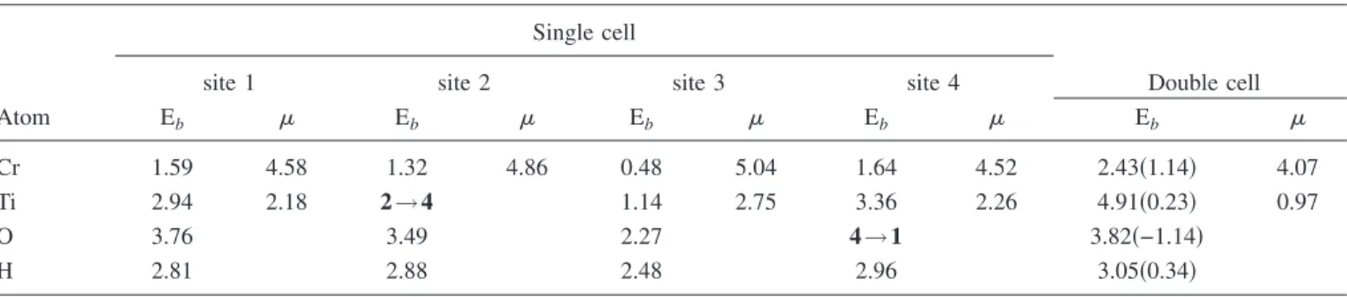
TABLE III. Calculated binding energies Eb共spin polarized for Cr and Ti and spin unpolarized for H and O systems兲 in eV and net
magnetic moment in BBohr magneton per adsorbate atom of individual atoms adsorbed on a possible four adsorption sites in a single cell and the most favorable binding site for a double cell of Mo6Se6nanowire. Values in parentheses are the binding energies calculated relative to bulk or molecular energies of adatoms.
Atom
Single cell
Double cell
site 1 site 2 site 3 site 4
Eb Eb Eb Eb Eb
Cr 1.59 4.58 1.32 4.86 0.48 5.04 1.64 4.52 2.43共1.14兲 4.07
Ti 2.94 2.18 2→4 1.14 2.75 3.36 2.26 4.91共0.23兲 0.97
O 3.76 3.49 2.27 4→1 3.82共−1.14兲
H 2.81 2.88 2.48 2.96 3.05共0.34兲
FIG. 6. 共Color online兲 The variation of the total energy of Cr6Se6with respect to the strain zz along the wire axis. Energy values indicated by square and filled circles correspond to the uni-formly and irregularly elongating wire, respectively. The atomic structure of uniformly and irregularly elongating wires are given by left and right insets, respectively. The force variation of uniformly elongating wire is shown by empty circles. The maximum of force variation corresponds to the inflection point of the energy.
We have considered four different possible adsorption sites in a single cell and one site 共which is the most favorable case兲 in a double cell of Mo6Se6共see Fig. 7兲. In single cell calculations, the nearest adsorbate-adsorbate distance is equal to c0共4.44 Å兲, while this distance is 2c0in double cell
calculations. Therefore, single cell calculation allows a sig-nificant coupling between adjacent adatoms. This coupling is small in double cell configuration. Eb of adsorbate atom in single cell configuration is obtained from the following ex-pression:
Eb= ET关Mo6Se6兴 + E关A兴 − ET关Mo6Se6+ A兴, 共3兲
where ET关Mo6Se6兴 stands for the fully optimized total energy
of bare Mo6Se6 nanowire calculated in single cell, E关A兴 is
the energy of the chain of adsorbate atom A and
ET关Mo6Se6+ A兴 is the fully relaxed total energy of the single
adsorbate on Mo6Se6 nanowire. We note that E关A兴 is calcu-lated after removing the Mo6Se6wire from the unit cell, but by keeping A in the same position as in Mo6Se6+ A.41 The
binding energies Eb are obtained according to the lowest ground-state total energies共either magnetic or nonmagnetic兲 of both ET关Mo6Se6+ A兴 and E关A兴. Bare nanowire has a
non-magnetic ground state with zero net spin. All adsorbates studied here have positive Eb which corresponds to opti-mized stable structure with significant binding. Our results are summarized in Table III. Both single and double cell calculations give the same site as the energetically most fa-vorable site. The double cell calculations can be representa-tive for single adsorption. While the A-A coupling energy is normally excluded in the Eb, the indirect effect of the A-A coupling to the chemisorption energy has remained. The bond between A and Mo6Se6 is generally weakened due to
the charge transfer from the bond to the A-A atomic chain of adsorbates. In the present case, Ebfor Ti and Cr is 1.64 and 3.36 eV per atom, respectively. These values are smaller than those obtained for double cell calculations. Both wires have magnetic ground states with= 4.52 and 2.26Bfor Cr and Ti, respectively. In Ti adsorption, initial geometry shown in Fig.7共b兲 transforms to site 4 geometry shown in Fig. 7共d兲 after structural optimization is performed. In the H and O
cases, Eb is 2.96 and 3.76 eV, respectively. Initial site 4 ge-ometry changes to site 1 in adsorption of O. Binding of all adsorbates to site 3 is weaker than the other adsorption sites. It is also instructive to calculate the binding energies of ad-sorbates with respect to the total energies of bulk or molecu-lar phases of these atoms instead of free atom energies. In Eq.共3兲, we have taken E关A兴 as the total energy per atom for Cr and Ti crystals and molecular energy per atom for H and O. The resulting Ebis represented in TableIIIin parentheses for double cell configuration. Even for this definition, signifi-cant Ebis obtained except for O. For oxygen, the reaction is endothermic. In double cell calculations, the amount of change in net magnetic and Eb 共⌬Eb兲 with respect to single cell calculations are different for each adatom. Dramatic change of induced net magnetic moment and Ebis observed in Ti adsorption.⌬Eb is 1.55 eV for Ti and 0.84 eV for Cr. Initial structure of wire is not preserved upon adsorption. Bond distances at the proximity of the adatom are slightly disturbed. For example, the nearest Mo-Se in-plane bond length extends from 2.61 to 2.74 Å in the case of Cr absorp-tion and from 2.61 to 2.92 Å for the Ti case. Metallic behav-ior does not change by these adsorbates.
VII. CONCLUSION
We have found that not only Mo6Se6, but also transition
metal atoms in the same column as Mo and chalcogen atoms in the same column as Se can form Mo6Se6-type stable
nano-wires. All wires have a high binding energy and it increases with increasing 共decreasing兲 row number of metal 共chalco-gen兲 atoms. The molecular dynamics simulations performed at 500 K and relaxation after random displacement of atoms indicate the stability of these structures. The wires with Te as a chalcogen atom are semiconductors but the rest of the fam-ily is metallic. Band structure for the bulk case gives rise to strong dispersion along wire axis. The calculated elastic stiff-ness constants point out that these wires are strong. Adatoms such as, O, H, Cr, and Ti atoms are also strongly bound to the Mo6Se6wire. Among them, Cr and Ti induce magnetic
mo-ment.
in共b兲; adatom is bound to Se atom 共red兲 in 共c兲, and in the same plane as Mo3Se3unit in共d兲.
*Electronic address: [email protected]
1S. Ciraci, A. Buldum, and I. P. Batra, J. Phys.: Condens. Matter 13, R537共2001兲.
2H. Ohnishi, Y. Kondo, and K. Takayanagi, Nature共London兲 395, 780共1998兲.
3O. Gülseren, F. Ercolessi, and E. Tosatti, Phys. Rev. Lett. 80, 3775共1998兲.
4S. Iijima, Nature共London兲 354, 56 共1991兲; S. Iijima, T. Ichihashi, and Y. Ando, ibid. 356, 776共1992兲.
5M. S. Dresselhaus, G. Dresselhaus, and P. C. Eklund, Science of Fullerenes and Carbon Nanotubes共Academic, San Diego, CA, 1996兲.
6S. Ciraci, S. Dag, T. Yildirim, O. Gülseren, and R. T. Senger, J. Phys.: Condens. Matter 16, R1共2004兲.
7R. T. Senger, S. Dag, and S. Ciraci, Phys. Rev. Lett. 93, 196807 共2004兲.
8S. Dag and S. Ciraci, Phys. Rev. B 71, 165414共2005兲.
9S. Dag, E. Durgun, and S. Ciraci, Phys. Rev. B 69, 121407共R兲 共2004兲.
10Y. Zhang and H. Dai, Appl. Phys. Lett. 77, 3015 共2000兲; Y. Zhang, N. W. Franklin, R. J. Chen, and H. Dai, Chem. Phys. Lett. 331, 35共2000兲.
11M. Potel, R. Chevrel, M. Sergent, J. C. Armici, M. Decroux, and O. Fischer, J. Solid State Chem. 35, 286共1980兲.
12J. M. Tarascon, F. J. DiSalvo, and J. V. Warszczak, Solid State Commun. 52, 227共1984兲; and J. M. Tarascon, G. W. Hull, and F. J. DiSalvo, Mater. Res. Bull. 19, 915共1984兲.
13J. H. Golden, F. J. DiSalvo, J. M. Fréchet, J. Silcox, M. Thomas, and J. Elman, Science 273, 782共1996兲.
14B. G. M. Chew, J. H. Golden, B. A. Huggins, F. J. DiSalvo, and D. B. Zax, Phys. Rev. B 50, 7966共1994兲.
15L. Venkataraman and C. M. Lieber, Phys. Rev. Lett. 83, 5334 共1999兲.
16L. Venkataraman, Y. S. Hong, and P. Kim, Phys. Rev. Lett. 96, 076601共2006兲.
17F. J. Riberio, D. J. Roundy, and M. L. Cohen, Phys. Rev. B 65, 153401共2002兲.
18I. Vilfan, Eur. Phys. J. B 51, 277共2006兲.
19S. Gemming, G. Seifert, and I. Vilfan, Phys. Status Solidi B 243, 3320共2006兲.
20M. F. Yu, B. S. Files, S. Arepalli, and R. S. Ruoff, Phys. Rev. Lett. 84, 5552共2000兲.
21S. Ogata and Y. Shibutani, Phys. Rev. B 68, 165409共2003兲. 22A. Meden, A. Kodre, J. P. Gomilsek, I. Arcon, I. Vilfan, D.
Vr-banic, A. Mrzel, and D. Mihailovic, Nanotechnology 16, 1578 共2005兲.
23T. Yang, S. Okano, S. Berber, and D. Tománek, Phys. Rev. Lett. 96, 125502共2006兲.
24Xiubin Qi and Frank E. Osterloh, J. Am. Chem. Soc. 127, 7666 共2005兲.
25Xiubin Qi, Frank E. Osterloh, S. A. Barriga, J. A. Giacomo, and S. Chiang, Anal. Chem. 127共4兲, 1306 共2006兲.
26M. C. Payne, M. P. Teter, D. C. Allen, T. A. Arias, and J. D. Joannopoulos, Rev. Mod. Phys. 64, 1045共1992兲.
27Numerical computations have been carried out by using VASP software: G. Kresse and J. Hafner, Phys. Rev. B 47, R558 共1993兲; G. Kresse and J. Furthmuller, ibid. 54, 11169 共1996兲. 28P. Hohenberg and W. Kohn, Phys. Rev. 136, B864 共1964兲; W.
Kohn and L. J. Sham, Phys. Rev. 140, A1133共1965兲. 29D. Vanderbilt, Phys. Rev. B 41, R7892共1990兲.
30J. P. Perdew, J. A. Chevary, S. H. Vosko, K. A. Jackson, M. R. Pederson, D. J. Singh, and C. Fiolhais, Phys. Rev. B 46, 6671 共1992兲.
31M. Methfessel and A. T. Paxton, Phys. Rev. B 40, 3616共1989兲. 32H. J. Monkhorst and J. D. Pack, Phys. Rev. B 13, 5188共1976兲. 33The crystal structure of Se and Te have hexagonal lattices in
which the atoms are arranged in spiral chains oriented along the
z axis. S has face centered orthorhombic crystal structure.
34Calculated bulk cohesive energies and lattice constants are in agreement with experimantel values.
35C. Kittel, Introduction to Solid State Physics, 7th ed.共Wiley, New York, 1996兲.
36D. M. Ceperley and B. J. Alder, Phys. Rev. Lett. 45, 566共1980兲. 37E. Durgun, S. Tongay, and S. Ciraci, Phys. Rev. B 72, 075420
共2005兲.
38D. Sánchez-Portal, Emilio Artacho, José M. Soler, A. Rubio, and P. Ordejon, Phys. Rev. B 59, 12678共1999兲.
39S. Tongay, R. T. Senger, S. Dag, and S. Ciraci, Phys. Rev. Lett. 93, 136404共2004兲.
40H. Mehrez and S. Ciraci, Phys. Rev. B 56, 12632共1997兲. 41Since E关A兴 is not a single free atom energy, but the energy of an
atomic chain having lattice parameter of the cell, it includes the A-A coupling. Therefore A-A coupling is excluded from Eb.