PLASMONIC NANOPARTICLES BY LASER
DEWETTING of THIN METALLIC FILMS
A THESIS
SUBMITTED TO THE DEPARTMENT OF PHYSICS
AND THE GRADUATE SCHOOL OF ENGINEERING AND SCIENCE OF BILKENT UNIVERSITY
IN PARTIAL FULFILLMENT OF THE REQUIREMENTS FOR THE DEGREE OF
MASTER OF SCIENCE
By Seval Sarıtaş January, 2013
ii
I certify that I have read this thesis and that in my opinion it is fully adequate, in scope and in quality, as a thesis for the degree of Master of Science.
. Prof. Dr. Atilla Aydınlı
I certify that I have read this thesis and that in my opinion it is fully adequate, in scope and in quality, as a thesis for the degree of Master of Science.
. Assist. Prof. Dr. Coşkun Kocabaş
I certify that I have read this thesis and that in my opinion it is fully adequate, in scope and in quality, as a thesis for the degree of Master of Science.
. Assist. Prof. Dr. Alpan Bek
Approved for the Graduate School of Engineering and Science:
. Prof. Dr. Levent Onural Director of the Graduate School
iii
ABSTRACT
PLASMONIC NANOPARTICLES BY LASER DEWETTING of THIN
METALLIC FILMS
Seval Sarıtaş
M. S. in Physics
Supervisior: Prof. Dr. Atilla Aydınlı
January, 2013
In this work, formation of metal nanoparticles via laser induced dewetting and their plasmonic properties have been investigated. The effects of metal film, substrate type, laser power density and dwell time on dewetting phenomenon were analyzed. Silver and gold thin films were fabricated with thermal evaporation on various substrates. Next, they were characterized by the ellipsometry, UV-VIS spectroscopy and atomic force microscopy (AFM) as the characteristic of the thin film affects dewetting. Samples were then processed by a cw argon laser. Varying the dwell time and power density, Ag and Au nanoparticles with different morphology were obtained. At the final stages of dewetting, nanoparticles attained spherical shapes. Particle size distribution and length scale analysis were performed using the images obtained from scanning electron microscope (SEM). Using these results, relations between the average particle size and film thickness, as well as the relation between length scale and film thickness were obtained to verify the occurrence of dewetting. Substrate and film type were observed to affect the particle morphology and particle size. Moreover, plasmonic resonance effect of Ag and Au nanoparticles were observed via the optical absorbance measurements. Multilayered metallic nanoparticles and embedded nanoparticles were fabricated and were found to display plasmonic properties.
iv
ÖZET
LAZER TOPAKLANMA YOLUYLA İNCE METAL FİLMLERDEN
PLAZMONİK NANO PARÇACIK OLUŞUMU
Seval Sarıtaş
Fizik, Yüksek Lisans
Tez Yöneticisi: Prof. Dr. Atilla Aydınlı
Ocak, 2013
Bu çalışmada, lazer topaklanma yoluyla plazmonik nano parçacıkların oluşumu ve onların plazmonik özellikleri incelenmiştir. Metal film, alttaş tipi, lazer güç yoğunluğu ve ışınlama süresinin topaklanma olayı üzerine etkisi analiz edilmiştir. Thermal buharlaştırmayla farklı alttaşlar üzerine gümüş (Ag) ve altın (Au) ince filmler üretilmiştir. Daha sonra, elipsometre, UV-VIS spektroskopi ve atomik kuvvet mikroskopu (AFM) ile karakterize edildiler çünkü ince filmlerin karakteristik özellikleri topaklanmayı etkilemektedir. İnce filmler karakterize edildikten sonra, farklı alttaşlar üzerindeki metal ince filmler sürekli argon lazer ile tavlandı. Işınlama süresi ve güç yoğunluğu değiştirilerek farklı morfolojide Ag ve Au nano parçacıklar elde edildi. Topaklanmanın son safhasında küresel şekle eriştiler. Taramalı alan mikroskopunun (SEM) imajlarından parçacık boyutu ve parçacıklar arası mesafe analizi yapıldı. Topaklanmanın varlığını doğrulamak için parçacık boyutu ve ince film kalınlığı arasındaki ilişki aynı zamanda parçacıklar arasındaki mesafe ve ince film kalınlığı arasındaki ilişki bu veriler kullanılarak elde edildi. Alttaş ve film tipinin parçacık morfolojisini ve parçacık büyüklüğünü etkilediği gözlemlendi. Ayrıca, soğurma ölçümüyle Ag ve Au nano parçacıkların plazmonik etkileri gözlemlendi. Çoklu tabaka metalik nano parçacıklar ve gömülü nano parçacıklar üretildi ve plasmon özellikleri gösterdikleri bulundu.
v
Acknowledgement
Besides my efforts, this thesis was completed with the encouragement and guidelines of many valuable people.
I would like to present my deepest gratitude to my academic advisor Prof. Atilla Aydınlı who expertly guided me during two years of my research period. He helped to develop my scientific mind and his firm enthusiasm for physics kept me constantly motivated to my research.
I would also present my gratitude to Assist. Prof. Dr. Coşkun Kocabaş and Assist. Prof. Dr. Alpan Bek for their valuable criticism as the members of my thesis committee.
I would like to thank Dr. Emel Sungur Özen for her enlightening mentorship and advices in all stages of my work, and also for invaluable contributions to this thesis.
I would like to thank my family for their care and support at all stages of my life and also thank my brother Serdar Sarıtaş who encouraged me in my determination to choose physics and to realize my potential.
I would like to thank my „‟laboratory partner‟‟ (Sinan Gündoğdu) for his support and friendship.
I would like to thank my „‟ fellow sufferer‟‟ (Melike Gümüş) for valuable friendship and trusts in me in all respect.
I would like to thank my officemates Abdullah Muti, Ertuğrul Karademir and Simge Ateş for creating less stressful working environment.
This work was supported in part by Turkish Scientific and Technical Research Council (TUBITAK), under grants no: 110T589 and 109R037
vi
Contents
1 Introduction 1
2 Background 5
2.1 Optical properties of metallic thin films . . . 6
2.2 Absorption and scattering of light by a nanoparticle . . . 9
2.3 Absorption and scattering by a conducting sphere . . . 11
2.3.1 Rayleigh scattering . . . 12
2.3.2 Mie scattering . . . 14
2.4 Nanoparticle formation . . . 15
3 Thin film deposition and characterization 21
3.1 Thermal evaporation of thin metallic films . . . 21
3.2 As grown film characterization . . . 22
3.2.1 Determination of the thickness and complex index of refraction . . 22
3.2.2 Determination of the optical constants of thin films . . . 28
3.2.3 Absorbance properties of Ag and Au thin films . . . 31
3.2.4 Surface characterization of thin films . . . 34
4 Nanoparticle formation by cw laser processing 36
4.1 Experimental set up . . . 36
4.2 SEM images of processed sample . . . 37
4.3 Surface characterization of processed sample . . . 53
5 Plasmonic properties of nanoparticles 56
5.1 The effect of particle size on plasmon resonance frequency . . . 56
5.2 The effect of embedding nanoparticles on plasmon resonance . . . 57
5.3 The effect of multilayered particles on plasmon resonance . . . 59
vii
viii
List of Figures
Figure 2. 1 (a) Imaginary and (b) real part of the dielectric constant for gold
according to the Drude-Sommerfeld free eleSctron model [11]. ... 8
Figure 2. 2 (a) Imaginary and (b) real part of the dielectric constant for gold
according to the Lorentz model [11]. ... 8
Figure 2. 3 Scattering of light by a nanoparticle. ... 9
Figure 2. 4 Free energy versus film thickness for different phase region
[19]. ... 17
Figure 2. 5 Shematic of dewetting (S<0) and spreading (S>0). ... 17
Figure 3. 1 Schematic of the evaporation chamber. ... 22
Figure 3. 2 Model used to fit the data from ellipsometric measurements. . 24
Figure 3. 3 Measured ellipsometric angle ψ as a function of wavelength and
simulation for the fit of the model to the data for 25.2 nm thick Ag
film on SiO
2, sample measured directly after evaporation…………. 25
Figure 3. 4 Measured ellipsometric ψ as a function of wavelength and
simulation for the fit of the model to the data for 25.2 nm thick Ag
film on SiO
2measured 7 days after evaporation. ... 25
Figure 3. 5 Measured ellipsometric angle ψ as a function of wavelength and
simulation for the fit of the model to the data for 25.2 nm thick Ag
film on SiO
2measured 10 days after evaporation. ... 26
Figure 3. 6 Oxide thicknesses of the 25.2 nm thick Ag/SiO
2thin film as a
function of air exposition time. ... 27
Figure 3. 7 Oxide thicknesses of the 18.9 nm thick Ag/SiO
2thin film as a
function of air exposition time. ... 27
Figure 3. 8 Measured ellipsometric angle ψ as a function of wavelength and
simulation for the fit of the model to the data for 23.8 nm thick Au
film on SiO
2sample. ... 28
ix
Figure 3. 9 Wavelength dependence of the refractive index (n) of Ag/SiO
2sample for different Ag film thicknesses (18.8 nm, 20.3 nm and 25.2
nm). ... 29
Figure 3. 10 Wavelength dependence of extinction coefficient (k) of
Ag/SiO
2sample for different Ag film thicknesses (18.8 nm, 20.3 nm
and 25.2 nm). ... 29
Figure 3. 11 Wavelength dependent refractive index (n) of Au/SiO
2sample
for different Au film thicknesses (14.1 nm, 19.2 nm, 23.8 nm). ... 30
Figure 3. 12 Wavelength dependent extinction coefficient (k) of Au/SiO
2sample for different Au film thicknesses (14.1 nm, 19.2 nm, 23.8 nm).
... 30
Figure 3. 13 Absorbance of as grown Ag/SiO
2sample for different
thicknesses (8 nm, 12.2 nm, 18.8 nm, 25.2 nm, 33.6 nm). ... 31
Figure 3. 14 Absorbance at 1000 nm of as grown Ag/SiO
2samples for
different film thicknesses (8 nm, 12.2 nm, 18.8 nm, 25.2 nm, 33.6
nm). ... 32
Figure 3. 15 Absorbance of as grown Au/SiO
2sample for different film
thicknesses (4.1 nm, 14.1 nm, 19.2 nm, 23.8 nm). ... 33
Figure 3. 16 Absorbance at 1000 nm of as grown Au/SiO
2sample for
different thicknesses (d=4.1 nm, 14.1 nm, 19.2 nm, 23.8 nm). ... 33
Figure 3. 17 AFM measurement for 8 nm (a) Ag/SiO
2(b) Ag/Si (c)
Ag/fused silica and for 10 nm (d) Au/SiO
2(e) Au/Si (f) Au/fused
silica. ... 35
Figure 4. 1 Experimental set- up for laser processing of thin metal films. 37
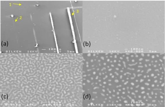
Figure 4. 2 SEM images of 11.5 nm Ag/SiO
2processed by cw Ar
+
laser
operating at 488 nm with 7.73 kW/cm2 power density. (a) SEM
images of the irradiated lines (b) SEM images of as grown region (c)
SEM images of line 2 which is a region irradiated at 70 ms dwell time
(d) SEM images of line 3 which is a region irradiated at 300 ms dwell
time. ... 38
x
Figure 4. 3 The threshold power density to observe the dewetting
phenomenon on different film thickness of Ag/SiO
2(9.7, 15.65, 23.9
nm). ... 39
Figure 4. 4 The threshold power density to observe the dewetting
phenomenon on different film thickness of Ag/fused silica (10, 15, 20,
25 nm). ... 39
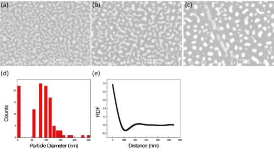
Figure 4. 5 SEM images of 12.2 nm Ag/SiO
2irradiated with cw Ar
+
laser
lasing at 488 nm with 3 kW/cm
2power density and (a) 56 ms dwell
time (b) 93 ms dwell time (c) 560 ms dwell time. d-e) size distribution
and radial distribution function obtained from SEM image in (c). .... 41
Figure 4. 6 SEM images of 18.9 nm Ag/SiO
2irradiated with cw Ar
+
laser
lasing at 488 nm with 5 kW/cm
2power density and (a) 56 ms dwell
time (b) 93 ms dwell time (c) 560 ms dwell time d-e) size distribution
and radial distribution function obtained from SEM image in (c). .... 41
Figure 4. 7 SEM images of 25.2 nm Ag/SiO
2irradiated with cw Ar
+
laser
lasing at 488 nm with 6 kW/cm
2power density and (a) 56 ms dwell
time (b) 93 ms dwell time (c) 560 ms dwell time. d-e) size distribution
and radial distribution function obtained from SEM image in (c). .... 42
Figure 4. 8 (a) Average particle diameter of Ag nanoparticles on glass
samples. The experimental data fits to h
(5/3)dependence and (b) length
scale of Ag nanoparticles on glass samples the experimental data fits
to h
2, where h is the thickness of the thin films. ... 43
Figure 4. 9 SEM images of 10 nm Ag/fused silica irradiated with cw Ar
+laser lasing at 488 nm with 21.7 kW/cm
2power density and (a) 28
ms dwell time (b) 112 ms dwell time (c) 700 ms dwell time d-e) size
distribution and radial distribution function obtained from SEM image
in (c). ... 44
Figure 4. 10 SEM images of 15 nm Ag/fused silica irradiated with cw Ar
+laser lasing at 488 nm with 25.4 kW/cm
2power density and (a) 25 ms
dwell time (b) 100 ms dwell time (c) 625 ms dwell time d-e) size
distribution and radial distribution function obtained from SEM image
in (c). ... 44
xi
Figure 4. 11 SEM images of 20 nm Ag/fused silica irradiated with cw Ar
+laser lasing at 488 nm with 17.4 kW/cm
2power density and (a) 28 ms
dwell time (b) 112 ms dwell time (c) 700 ms dwell time d-e) size
distribution and radial distribution function obtained from SEM image
in (c). ... 45
Figure 4. 12 SEM images of 25 nm Ag/fused silica irradiated with cw Ar
+laser lasing at 488 nm with 26.1 kW/cm
2power density and (a)28 ms
dwell time (b) 112 ms dwell time (c) 700 ms dwell time d-e) size
distribution and radial distribution function obtained from SEM image
in (c). ... 45
Figure 4. 13 Figure 4. 13: SEM images of 8 nm Ag/Si irradiated with cw
Ar
+laser lasing at 488 nm with 20 ms dwell time and (a) 270 kW/cm
2power density (b) 302 kW/cm
2power density (c) 334 kW/cm
2power
density d-e) size distribution and radial distribution function obtained
from SEM image in (c). ... 46
Figure 4. 14 SEM images of 12.5 nm Ag/Si irradiated with cw Ar
+laser
lasing at 488 nm with 302 kW/cm
2power density and (a) 8 ms dwell
time (b) 40 ms dwell time (c) 125 ms dwell time d-e) size distribution
and radial distribution function obtained from SEM image in (c). .... 46
Figure 4. 15 SEM images of 24.6 nm Ag/Si irradiated with cw Ar
+laser
lasing at 488 nm with 20 ms dwell time and (a) 270 kW/cm
2power
density (b) 302 kW/cm
2power density (c) 334 kW/cm
2power density
d-e) size distribution and radial distribution function obtained from
SEM image in (c). ... 47
Figure 4. 16 The threshold power density to observe the dewetting
phenomenon on different film thickness of Au/SiO
2(13.6, 15.1, 19.6
nm). ... 49
Figure 4. 17 The threshold power density to observe the dewetting
phenomenon on different film thickness of Au/fused silica (12.1, 13.9,
18.8 nm). ... 49
Figure 4. 18 SEM images of 13.6 nm Au/SiO
2irradiated with by cw Ar
+
xii
kW/cm
2power density (b) 16.7 kW/cm
2power density (c) 39.3
kW/cm
2power density d-e) size distribution and radial distribution
function obtained from SEM image in (c). ... 50
Figure 4. 19 SEM images of 15.1 nm Au/SiO
2irradiated with by cw Ar
+
laser operating at 488 nm with 104 ms dwell time and (a) 23.2
kW/cm
2power density (b) 30.7 kW/cm
2power density (c) 92.7
kW/cm
2power density d-e) size distribution and radial distribution
function obtained from SEM image in (c). ... 50
Figure 4. 20 SEM images of 19.6 nm Au/SiO
2irradiated with by cw Ar
+
laser operating at 488 nm with 104 ms dwell time and (a) 39.3
kW/cm
2power density (b) 54.3 kW/cm
2power density (c) 126.3
kW/cm
2power density. ... 51
Figure 4. 21 SEM images of 12.1 nm Au/fused silica irradiated with by cw
Ar
+laser operating at 488 nm with 104 ms dwell time and (a) 15.0
kW/cm
2power density (b) 19.9 kW/cm
2power density (c) 26.7
kW/cm
2power density d-e) size distribution and radial distribution
function obtained from SEM image in (c). ... 51
Figure 4. 22 SEM images of 13.9 nm Au/fused silica irradiated with by cw
Ar
+laser operating at 488 nm with 104 ms dwell time and (a) 26.7
kW/cm
2power density (b) 30.7 kW/cm
2power density (c) 43.9
kW/cm
2power density d-e) size distribution and radial distribution
function obtained from SEM image in (c). ... 52
Figure 4. 23 SEM images of 18.8 nm Au/fused silica irradiated with by cw
Ar
+laser operating at 488 nm with 104 ms dwell time and (a) 75.3
kW/cm
2power density (b) 131.9 kW/cm
2power density (c) 169.6
kW/cm
2power density. ... 52
Figure 4. 24 AFM images of (a)10 nm (b) 15 nm (c) 20 nm Ag thin film on
glass irradiated with cw Ar
+laser (at all lines configuration). ... 54
Figure 4. 25 The comparison of AFM and SEM images of 8 nm Ag/SiO
2irradiated with cw Ar
+laser (all lines configuration). (a)AFM image
(b) SEM image (c)3D view of AFM image. ... 54
Figure 4. 26 AFM images of (a)13.6 nm (b) 15.1 nm (c) 19.6 nm Au thin
xiii
Figure 5. 1 Absorbance measurements of the 10 nm, 15 nm, and 20 nm
thick Ag/SiO
2samples irradiated by 25.2 kW/cm
2power density and
336 ms dwell time. ... 57
Figure 5. 2 Absorbance measurement of embedded nanoparticles.how
much shift in each case ... 58
Figure 5. 3 Absorbance measurement of embedded nanoparticles. ... 59
Figure 5. 4 The optical microscope images of multilayered structure with
SiO
2layer. ... 60
Figure 5. 5 The absorbance measurement of multilayer nanoparticle
xiv
List of Tables
3.1 Lorentz model parameters [27] . . . 23 3.2 AFM measurement . . . 35 4.1 Particle size and length scale for different thickness of Ag on glass samples . . . . 42 4.2 Heat capacity and thermal conductivity for different substrates . . . 47 4.3 The size of the particle at the vertical direction . . . 53 4.4 The size of the particle at the vertical direction . . . 55
1
Chapter 1
1.
Introduction
Metal nanoparticles have recently received a lot of attention due to many possible applications ranging from biochemical sensors to efficient solar cells. The presence of localized plasmons in the particles have led to research on fundamental interactions of two level quantum systems with electromagnetic fields such as exciton-plasmon interactions. The objective of this thesis is to study the laser dewetting of thin metal films to obtain metal nanoparticles with tunable plasmonic resonance upon laser processing for possible applications such as the study of exciton-plasmon interactions. Metal nanostructures show optical properties that are strikingly different from the properties of the bulk material. As is well known over the centuries and witnessed by beautifully stained glasses of many churches and mosques, the deep red and yellow colors in stained glass are caused by small metal particles of gold and silver. Despite the systematic work of Faraday on nanoparticles where he recognized that the optical properties of bulk gold and colloidal gold are different and the color of gold changes depending on the size of the nanoparticles as far back as 1857 it is only in 1950‟s that the origin of this behavior is started to be understood as the results of collective oscillations of free electrons. In contrast with experimental work, the theory of optical properties of metal nanoparticles was developed by Gustav Mie as early as 1908. To explain the interaction of nanoparticles with light, he solved Maxwell‟s equations, assuming metal nanoparticles as spherically symmetric conducting objects. In recent years, Mie‟s approach was extended to other geometries such as metallic cylinders and disks.
There are many ways to obtain nanoparticles using experimental techniques such as sputtering, e-beam lithography (EBL) and dewetting. With EBL, size and shape of metal nanoparticles can be controlled [1] but this is a tedious and expensive procedure. Sputtering is simple and controllable in particle‟s size distribution [2]. However, the control of growth parameters is difficult in this process. The method of dewetting is easier. Dewetting can be described as the rupture of a thin liquid film on a substrate upon perturbation by an external source of energy. Alternatively, dewetting is the phenomenon describing formation of droplets from continuous thin films. Thin films are generally metastable in their as deposited state and can dewet to form islands when
2
the sample is appropriately heated. The driving force for dewetting is the minimization of the total energy of the free surface of the film and substrate, and of the film-substrate interface. This can, for example, be achieved by thermal or laser annealing. Bischof et al. analyzed the laser induced dewetting phenomenon of thin liquid metal films [3]. Later, Krishna et al. analyzed pulsed laser induced dewetting phenomena and obtained spherical silver naoparticles with predictable size distribution [4]. In addition, Wenyu Huang et al. reshaped prismatic Au nanoparticles in periodic monolayer arrays by femtosecond laser processing and they obtained spherical nanoparticles due to dewetting phenomenon [5]. There are many applications of metallic nanostructures such as surface enhanced spectroscopy (surface enhanced Raman scattering (SERS) and surface enhanced fluorescence) or absorption enhancement in solar cells. The appeal of metal nanoparticles for such application arises from large electromagnetic field enhancement associated with these metallic structures. The conduction electrons oscillate with under the influence of applied electromagnetic field. In the case of Raman spectroscopy, large enhancement factors as high as 1014 could be obtained from the silver and gold nanoaggregate cluster structures. Such large enhancements allow Raman measurements of single molecules even under nonresonant conditions [6]. Metallic nanostructures are also used for thin film solar cells to increase efficiency. Stuart and Hall put dense nanoparticle arrays on Si-on-insulator photodetector structures and increased the photocurrent in the infrared region by scattering light from metallic nanoparticles [7]. Later, Pillai et al. analyzed effects of particle size on efficiency using the same geometry with the silver nanoparticle array on silicon-on-insulator cell. They concluded that small silver nanoparticle increases efficiency both in the visible and in infrared region [8]. In addition, the shape of nanoparticles affects field enhancemement. Akimov and Koh also analyzed silver nanoparticle on ITO layer for thin-film a-Si:H solar cell. They studied effect of shape of the nanoparticle on light absorption for both resonant (silver) and nonresonant (aluminum) case. They found that spherical nanoparticles increase efficiency more than other nanoparticle shapes [9]. Atwater et al. worked on different plasmonic light trapping geometries to increase efficiency of thin film solar cells. There are two types of field enhancement: First, absorption enhancement is achieved by light trapping due to the scattering from the metal nanoparticles. In this case, the geometry consists of metal nanoparticles at the surface of the solar cell. Second, light trapping is achieved by excitation of localized modes in metal nanoparticles embedded in the semiconductors [10]. Changing the particle size and shape, field enhancement can be obtained at different wavelengths which can allow a more efficient use of the solar spectrum.
3
In this work, our aim is to obtain Ag and Au nanoparticles with well defined shape and size as well as percolated Ag and Au distributions by cw Ar+ laser induced dewetting. We fabricated metallic nanoparticles using cw laser processing and characterized them using various analytical techniques. Metallic thin films were obtained by thermal evaporation of the relevant metals on different substrates such as silicon, glass and fused silica. We first, characterized as deposited thin films to obtain primarily the thickness of the films among others. Silver and gold nanoparticles on different substrates were obtained via laser induced spinodal dewetting and the dewetting phenomena was studied as a function of film thickness, laser power density and irradiation times. Different samples with several film thicknesses as well as embedded nanoparticles and multi-layer structures were fabricated and their differences were studied. This work is expected to lead to formation of periodic arrays of metallic nanoparticles for exciton-plasmon coupling and eventually to high efficiency light emitting structures and photovoltaics.
In Chapter 2, the interaction of light with metal is explained using simple models to reveal important features of which there are two. Optical properties of metals strongly depend on the complex dielectric function of used in the models, Drude-Sommerfeld and Lorentz oscillator, to the express the dielectric function. These models point to a resonance phenomenon, at what is known as the plasma frequency. Thus, parameters affecting resonance conditions are discussed. Moreover; absorption and scattering from metallic nanoparticles are discussed and two approaches, Mie and Rayleigh, are explained for spherical metal nanoparticles. In Chapter 2 dewetting phenomenon by which nanoparticles are obtained from thin metal films is also explained.
In Chapter 3, sample preparation methods as well as the experimental approach and setups used are described. As the backbone of thin film fabrication method, thermal evaporation is explained. Next, the characterization of as deposited samples is presented. The thickness of the as deposited films were determined as well as their optical constants by means of ellipsometric measurements. The absorption coefficient of different films is determined by UV-VIS spectroscopy and finally, the roughness of as deposited films were characterized by atomic force microscopy (AFM).
Chapter 4 gives details of experimental set-up used to process the samples. SEM images of annealed Ag and Au samples on different substrates are shown. Also analysis of particle size distribution and length scale, as a measure of average distance between two particles, were made from SEM images. Furthermore, AFM measurements were done
4
for annealed Ag on glass substrates for different thicknesses in order to measure average particle‟s size and compare it with the data obtained from SEM images. We showed that average particle size and length scale depend on the thicknesses of thin films. In addition, the effect of the thermal properties of metal and substrate on nanoparticle formation was indicated.
In Chapter 5, we analyze the effect of plasmon after annealing for different thickness of Ag on glass samples and the effect of particle size and shape on plasmon resonance curve is obtained. Embedded and multilayer samples are also studied and the effect of dielectric constant and its thickness on plasmon resonance curve is analyzed.
In the last part; after a brief conclusion, we illustrated the areas that can exploit the plasmonic properties of the nanoparticles.
5
Chapter 2
2.
Background
Metal nanoparticles have widely been used in plasmonic applications for local field enhancements and electromagnetic confinement. Due to coupling with incident light, the conduction electrons in metallic nanoparticles are driven into collective oscillations generating an electromagnetic field whose quanta is called the plasmon. Plasmon modes exist in various metals, most notably in noble metals such as gold and silver. The excitation of plasmons by light leads to strong light scattering and absorption and enhancement of the local electromagnetic field. Enhancement of oscillation amplitude at resonance of conduction electrons leads to the formation of greater electromagnetic field at some frequencies than at others. These frequencies are known as resonance frequencies. Resonance phenomenon depends strongly on the dielectric function of the metal and the environment. The presence of plasmons can be inferred from the frequency dependent dielectric function which can be studied using either of two models: Drude- Sommerfeld and Lorentz oscillator models. These models are one electron models and do not take into account finite size effects. In the case of small metallic particles, resonance is affected by the size of the nanoparticles, as well. The metal nanoparticle size effect on plasmon resonance can be analyzed via the electromagnetic scattering crosss-section and absorption cross-section of metallic nanoparticles. Mie and Rayleigh scattering are two approaches which show the effects of nanoparticle size and dielectric constant on plasmon resonance. We have used the dewetting phenomenon to produce nanoparticles with controllable size and shape. A factor affecting the dewetting phenomenon during laser processing of thin metallic films is the heat transfer which prepares the conditions for surface free energy minimization.
6
2.1. Optical properties of metallic thin films
In order to understand the optical behavior of the thin metallic films, we have to understand how metals interact with light. To describe the optical properties of metals there are two models. Drude-Sommerfeld model explains the behavior of conduction electrons and Lorentz oscillator model takes into account inter-band excitations of electrons. In the Drude-Sommerfeld model, the equation of motion for a conduction electron with a damping term under the influence of an external electric field, can be written as a damped and driven harmonic oscillator:
(1)
where x is the displacement of the electron, ω is the angular frequency of the incident light, and E0 is its amplitude. The second term shows the damping force of the medium.
For a harmonic oscillator, we can propose x as x(t)=x0e-iωt. By inserting the proposed
solution into (1), we find:
(2)
In order to find the relative dielectric constant, we can benefit from the definition of the electric displacement D which is defined as D=єrє0E(t) which can also be written as
D=є0E+ P where P is the polarization, defined as the field due to total number of electric
dipoles, –Nex, present in the medium. Using x as expressed in Eqn (2), we can obtain an expression for the relative dielectric constant from above equation as:
(3)
where ωp is defined as the plasma frequency with . For small damping
7
constant will be equal to ). It is clear from the previous equation that when the frequency of the driving field is equal to the plasma frequency, resonance is achieved. The resonance condition is satisfied when goes to zero. In this case, refractive index, , changes dramatically leading to optical loss or gain. These results clearly demonstrate that the absorption of incident electromagnetic field can drive the electrons at a resonance frequency where absorption is maximum. This, in fact, is observable in our experiments.
In the Lorentz oscillator model, same method used above for free electrons is applied for bound electrons. In this case, interband transitions occur. The equation of motion for a bound electron can be written as:
(4)
where m is the effective mass of bound electrons, Г is the damping constant for bound electron and α is the spring constant representing the strength of the potential. As a result, dielectric function is found as:
(5)
Here, is the plasma frequency for bound electrons and is the density of
the bound electrons and . In the visible region, correction needs to be made to the dielectric function as obtained from Drude-Sommerfeld model for noble metalsdue to the response of bound electrons. In the visible part of the electromagnetic spectrum, oscillating bound electrons have enough energy to be excited into the conduction band. As can be seen from figures 2.1 and 2.2, for gold interband transition is significant at wavelengths shorter than 650 nm [11].
8
Figure 2. 1 : (a) Imaginary and (b) real part of the dielectric constant for gold according to the Drude-Sommerfeld free electron model [11].
Figure 2. 2 : (a) Imaginary and (b) real part of the dielectric constant for gold according to the Lorentz model [11].
200 400 600 800 1000 -60 -50 -40 -30 -20 -10 0 R e ( ) Wavelength (nm) (b) 200 400 600 800 1000 0 1 2 3 Im ( ) Wavelength (nm) (a) 200 400 600 800 1000 -3 -2 -1 0 1 2 3 R e ( ) Wavelength (nm) (b) 200 400 600 800 1000 0 2 4 6 Im ( ) Wavelength (nm) (a)
9
Since they are one electron models, we can use these models not only for thin metallic films but also for metallic nanoparticles, as well. As mentioned above, dielectric constant determines the resonance frequency leading to absorption of incident electromagnetic field by electrons. Resonance frequency also depends on the particle size and shape [11-13]. We can observe size effects on resonance frequency in experiments by transmittance measurements.
In the next section, we will also analyze the effect of size and shape of the nanoparticle on absorption and scattering.
2.2. Absorption and scattering of light by a nanoparticle
The interaction of electromagnetic radiation with matter can be explained by Maxwell‟s equations. When a nanoparticle with an arbitrary shape is illuminated by an electromagnetic wave, light is reflected and refracted and part of the refracted wave is absorbed by the nanoparticle.
Figure 2. 3 :Scattering of light by a nanoparticle.
As a first approximation, metallic materials can be assumed to be as homogeneous and isotropic. Maxwell‟s equations are solved using boundary conditions appropriate for the nanoparticles. The solution of Maxwell‟s equations can be thought in terms of harmonic waves. To find the relation between the electromagnetic field inside the nanoparticle (E, H) and the electromagnetic field outside the nanoparticle (Einc, Hinc, Esca, Hsca), boundary
conditions at the surface of the nanoparticle have to be used. There are two boundary conditions arising from tangential continuity of fields:
Einc, Hinc E, H є, σ Esca, Hsca єm єm
10
(6)
(7)
where n is the vector normal to the surface and subscripts inc and sca describe the incident and scattered component of E and H. Apart from these boundary conditions, there is additional boundary condition covering continuity of the normal component of E:
(8)
By calculating the electromagnetic fields, we can also calculate rate of energy flux where part of the energy of incoming light is scattered or absorbed. The rate of energy flux for a closed volume V containing the particle can be expressed as:
(9)
where W is the energy density, S= E x H is the Poynting vector which describes the radiant energy flux density. From the conservation of energy, in the stationary case, where , the radiant flux outside the particle, divS, has to be equal to the total energy loss in the particle by absorption, J.E.
Absorption rates consist of three terms, which are Wo, Wext, and Wsca. Wo is the rate of
energy absorbed from the incident wave in the integrating volume when there is no particle. This term is used to take into account of absorbing embedding media. Wext is
the extinction rate and Wsca is the scattering rate. The relationship between them can be
expressed as:
11
The optical scattering and absorption cross-sections [13] are useful quantities to describe effect of the size, the shape, and the wavelength on scattering and absorption by various nanoparticles. To find the optical scattering and absorption cross-section, σ, the rates of energy transfer to various processes are divided by incident intensity, I0.
(11)
The optical scattering and absorption cross-sections are useful to compare the size, shape and wavelength dependencies of the scattering and absorption by various nanoparticles. As the analytical solutions to Maxwell‟s equations are only possible for geometrical shapes, snumerical approaches are used for arbitrary shapes. In the next section, cross-sections will be expressed for spherical nanoparticles to understand the effect of the particle size on absorption and scattering by nanoparticles.
2.3. Absorption and scattering by a conducting sphere
It is simpler to model the nanoparticle as a sphere. In a metal, there are fixed positive ions and equal amount of free electrons. When the metal is illuminated with light, free electrons shift their spatial positions but positive ions exert a restoring force in the opposite direction. Therefore, free electrons start to oscillate. The frequency of oscillation is affected by the density of electrons, the size and the shape of the charge distribution. Depending on the metal nanoparticle‟s size, there are two types of collective oscillations called coherent and incoherent. The validity of one as opposed to the other is decided according to the ratio of the particle size to the wavelength of the incident light. For small ratios at visible wavelengths, with the typical size limit of about 300 nm, oscillations will be coherent. In coherent oscillations, the dipole modes are dominant [13]. The collective oscillations in this model is known as dipole plasmon resonance. If the ratio increases, higher order modes will be dominant and the oscillations will be incoherent.
In the next section, plasmon resonances are evaluated as a function of the size of spherical metal nanoparticles. For small nanoparticles Rayleigh scattering and for nanoparticles bigger than the said limit, [(2πr)/λ<<1 where r is the characteristic dimension of nanoparticle], Mie scattering will be considered.
12
2.3.1. Rayleigh scattering
Rayleigh scattering is the scattering of light from particles whose size is much smaller than the wavelength of the light. In this case, electromagnetic field is approximated to the near field zone kr << 1. In this type of scattering, incident electric field can be thought as being constant across the particle due to neglecting retardation effects, which means that all points of a nanoparticle respond simultaneously to an incoming electromagnetic field.
To find the electric field inside and outside of the spherical metal nanoparticles, Poison equation ∇2Φ=-4πQ(r) should be solved. If there is no net charge outside the metal nanoparticle, this equation turns into Laplace equation, ∇2Φ=0. Electric potential, Φ, is found inside and outside of particle from the solution of Laplace‟s equation. We can also obtain electric field inside the particle (E1) and electric field outside the particle
(E2) from the relation E= -∇Ф. For a spherical nanoparticle with radius , solutions
from electromagnetic theory textbooks can be found as:
(12)
(13)
where r is the radial distance, θ is the polar angle, E0 is the external field and x is the
direction of it. These equations imply that electric field is strongly localized at the surface of the particle at the resonant condition, that is: (ε1+ε2) is a minimum. As
mentioned earlier, these equations are used to calculate optical scattering and absorption cross-section which are the useful terms to understand the effect of size and shape of sphere to the scattering and absorption. For scattering cross-section radiated energy rates is divided by intensity and for absorption cross section dissipated energy rates is divided by intensity. Both the scattering and absorption cross-sections can be expressed in terms of polarizability, α(ω), as [13]:
13
(15)
Polarizability is related to the electric dipole moments in the nanoparticle and is defined
in terms of dipole moments as . The first term in the equation for the
outside electric field is the applied field but the second term is the induced dipole field. Thus the outside potential will be as:
(16)
where the dipole moment and polarizability are given as [11]:
(17)
(18)
As seen in the Eqns 14 and 15, scattering and absorption cross-sections are dependent on polarizability and polarizability depends on particle size, , as presented by in Eqn (18). It is clear that the smaller the particle size, the smaller are the absorption and scattering cross sections.
If the particle is small, only the dipole moment is present. In larger particles, higher terms of moment such as quadrupole and octupole moments cannot be ignored. However, larger particles need rigorous solutions in order to include higher order moments in the solutions. In this respect, Mie theory is more useful. In the next part, Mie theory will be summarized.
14
2.3.2. Mie scattering
In Mie theory, incident wave is assumed to be a plane wave and due to the symmetry of sphere a direction of propagation is chosen as z-axis. In this case the electromagnetic potential is found from Laplace‟s equation in terms of Legendre polynomials as (see “Classical Electrodynamics”, J. D. Jackson).
(19)
where r, θ and φ are the spherical coordinates, zn(kr) is the quantity that can be any of
the spherical Bessel functions which are spherical Bessel functions jn, spherical
Neumann functions γn, Henkel functions of the first kind , and of the second kind
for n=1, 2,…, ∞. The above equation suggests that there are many different solutions due to the indices n and m. Due to the spherical symmetry, m can only have values of -1 and +1. In this equation cos(mφ) comes from even solution and sin(mφ) comes from odd solution. The electromagnetic field in any polarization can be expressed in terms of plane of incidence and it can be the superposition of the two orthogonally polarized waves which are transverse magnetic (TM) and transverse electric (TE). In the TM mode, there is no radial component of the magnetic field and in the TE mode there is no radial component of electric field.
To find the optical scattering and absorption cross-sections, energy transfer rates similar to the case in Rayleigh scattering, are used. Using spherical coordinates, the energy transfer rates are found as:
(20)
15
(22)
where W0 is the absorption rate in the absence of the sphere, Wext is the extinction rate
and Wsca is the scattering rate. Rcs represents the radius of a concentric sphere which is
bigger than the radius of spherical particle. This is a conceptual radius representing the integration surface. If the rates are divided by intensity I0, cross-section, σ, is obtained.
Consequently, cross-sections are equal to:
(23)
(24)
where, an and bn are the scattering coefficients and they are size dependent and, kM is
the wavenumber. This is valid both the far-field zone (kr >> 1) and the near-field zone (kr << 1) because cross-section is independent from the Rcs [14]. Thus scattering and
extinction cross-sections obtained via Mie theory can be used to analyze the effect of the size and the shape of a particle on absorption and scattering.
2.4. Nanoparticle formation
There are many ways to obtain nanoparticles, such as dewetting, electron beam lithography (EBL), sputtering, and thermal evaporation. Our aim is to obtain nanoparticles with controllable size and shape. Although sputtering and thermal evaporation are relatively simple methods, there are several parameters affecting nanoparticle formations [15]. With EBL method, the size and shape of nanoparticles can be controlled but this is a sophisticated, time consuming and expensive approach and can only be done over very small areas [16]. In this work, we preferred the quick and simple method of laser dewetting which can be scaled up to very large areas. Laser
16
processing has the added advantage of spatial localization of the processed area as well as having low thermal budget [17].
Dewetting has received a lot of interest for nanoscale pattern formation because it is a predictable and robust process. Large scale applications such as in solar industry, dewetting is the proper fabrication method due to the simplicity of the process. There are some parameters affecting the process such as annealing time, thickness and type of the film, type of the substrate that affect the resulting nanoparticle size, shape and distribution.
Dewetting process is initiated from the instabilities of a thin fluid film. During this process, once formed, the thin liquid film on the substrate is ruptured and droplets are obtained [18]. If two or more components of a thin film decomposes into two distinct regions such as air and silver we can talk about spinodal decomposition. Spinodal decomposition occurs uniformly throughout the material and not only at certain nucleation sites. Thermodynamically unstable thin film-substrate systems are candidates for spinodal dewetting [3]. In these systems, the region with negative curvature of the free energy versus thickness curve defines the unstable region [19]. There are three distinct regions (phases) which are labeled as stable, metastable and unstable under the curve (Fig. 2.4). In these regions, components can have different chemical compositions and physical properties. Dewetting can also be expressed in terms of a spreading coefficient, S, defined as the free energy difference between a solid in contact with vapor and a solid covered by thick liquid layer and can be shown to be as [20]:
(25)
where referring to Fig 2.5, γB is the substrate B-vapor surface tension, γA is the liquid A-
vapor surface tension and γAB is the substrate B- liquid A surface tension. When S>0,
liquid A spreads completely on substarate B and when S<0 which is the lower energy configuration, liquid A turns into droplets on substrate B, in other words, dewetting occurs.
17
Figure 2. 4 :Free energy versus film thickness for different phase region [19].
Figure 2. 5: Shematic of dewetting (S<0) and spreading (S>0).
Free energy (F) is the sum of the surface/interface energies, external energy and volume energy. Interfacial energies are expressed by interfacial tensions and external energy is the gravitational energy. In addition, for volume energy, we have to take into account contribution of the intermolecular forces. In the case of apolar film on apolar substrate, intermolecular force is the long range dispersion force (Van der Waals). Therefore, free energy can be shown as:
1E-10 1E-9 1E-8 1E-7 1E-6 1E-5 1E-4 1E-3 0,01 1 2 3 4 5 F re e Ene rg y (J/ m 2 ) Film Thickness (nm) Unstable Metastable Stable
18
(26)
where is the thickness, is the density of the film, g is the gravitational acceleration and P(h) is the energy related intermolecular force. If we consider P(h) to be dominated by Van der Walls interactions, the interaction energy varies as 1/h6 and integrated over the plane of the surface we have [4]:
(27)
where A is the Hamaker coefficient which determines the sign and magnitude of the interaction between the substrate-film and film-vacuum interface. The Hamaker coefficient, A, can be calculated using a relationship which is a function of the frequency dependent dielectric coefficients of the different media, which is summed over the entire frequency regime and is proportional to (ε1 – ε2). (ε2 – ε3), where ε1, ε2,
and ε3 are the dielectric functions of substrate, film, and vacuum, respectively. Typical
values for Hamaker coefficients are in the order of 10-19 J [21].
Dewetting can occur in three different ways: i) Homogeneous nucleation and growth, ii) heterogeneous nucleation and growth of droplets, and iii) droplet formation during thin film hydrodynamic (TFH) instabilities. In homogeneous nucleation there is no characteristic length scale i.e., holes are randomly distributed. However, heterogeneous nucleation and growth is due to defects, impurities or other heterogeneities so that nucleation starts where defects are. Ideally, a characteristic length scale can be obtained with ordered nucleation sites. Dewetting of spinodally unstable systems is an example of dewetting which is due to the thin film hydrodynamic (TFH) instabilities. Spinodal dewetting initiated by the thermal fluctuations at the surface of the thin liquid film [22]. In this type of dewetting there is a characteristic length scale and particle size which are proportional to square of film thickness and (5/3) power of the thickness, respectively. Spinodal dewetting occurs when the curvature of free energy is smaller than zero. The morphological changes due to dewetting reduce the free energy of the film-substrate-vapor system, the system then enters into a stable regime. Free energy per unit area can be written as [4]:
19
Volume free energy comes from the van der Waals interaction between nonpolar atoms. If the free energy curvature as a function of film thickness is negative, the film is in the unstable region and, spinodal dewetting can occur.
Benefiting from the lubrication theory, which gives the relation between the mass flux and effective pressure gradient which comes from the perturbation producing the interface curvature and disjoining pressure due to van der Waals interactions, spinodal dewetting can be analyzed. Disjoining pressure has been expressed as A/6 (h‟)3 where h‟ is the instantaneous film thickness. The dynamical equation is as shown below [23]:
(29)
where η is the viscosity and γ is the interfacial energy of the film vacuum interface and A*=A/2π. If h is perturbed, h‟ will be equal to h + h* so the above equation will become: (30)
Substituting normal mode form h*=ε exp (ikxx + ikyy + σ t) where σ shows the growth
or decay rate of perturbations and if , then will be obtained where km
is the fastest growing mode. Thus; the characteristic length scale, Λ=2π/km, becomes:
(31)
This result can be confirmed using statistical methods on the distribution of droplets to calculate length scale.
20
The diameter of the particle (D) can be found from volume conservation [24]. Volume of the particle is approximated as cylinder with diameter R and thickness h. According to volume conservation [25]:
(32)
where f (θ) is a geometric factor and depends on the particle contact angle (θ). Using the length scale, Eqn. 3, we can find particle diameter as:
21
Chapter 3
Thin film deposition and
characterization
In this work, we chose Ag and Au thin films for nanoparticle formation to observe their plasmonic effects. The plasmon resonance frequency of the Ag and Au is in the visible part of the electromagnetic spectrum. To begin with, we have prepared thin films by thermal evaporation and then we obtained metallic nanoparticles by laser induced dewetting. The dewetting phenomenon depends on the initial thin film‟ characteristics; we, therefore, characterized the as deposited thin films first.
3.1. Thermal evaporation of thin metallic films
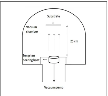
Thermal evaporation is one of the most commonly used metal deposition techniques. There are two types of thermal evaporation techniques: resistance heating and electron beam heating. In this work, we used resistance heating technique which consists of vaporizing a solid material (pure metal in our case) by heating it to sufficiently high temperatures and recondensing it onto a cooler substrate to form a thin film. As the name implies, heating is carried out by passing a large current through a tungsten boat which has a finite electrical resistance (figure 3.1). The chamber pressure is an important parameter, as at high pressure the metal vapor can intereact with atmosphere but if the pressure is small enough, the evaporated atoms will move in straight lines towards the substrate. The depositions were performed at pressure of 10-6 Torr and the sample was placed at 25 cm above the source. All the samples were prepared at the same deposition rate of 1 Å/ sec.
22
Figure 3. 1:Schematic of the evaporation chamber.
3.2. As grown film characterization
3.2.1. Determination of the thickness and complex index of refraction
Determination of the thickness and the complex index of refraction of Ag and Au films is important for further processing of these films. The as deposited Ag and Au thin films were analyzed using ellipsometry which is a sensitive optical technique for analyzing the characteristics of surfaces and thin films. The ellipsometer is sensitive to changes in the polarization state of the reflected light. If linearly polarized light is reflected from the sample obliquely, the reflected light becomes elliptically polarized. Direction of incident light, reflection properties of sample and angle of incidence affect the shape and the orientation of the ellipse. By analyzing the polarization of the reflected and the incident light, we can find the phase change (∆) and the relative amplitude ratio (tanψ) upon reflection. By measuring ellipsometric angles, ∆ and ψ, we can deduce the thickness of the thin film. For this purpose, we used J. A. Woollam variable angle spectroscopic ellipsometer (VASE) in the wavelength range of 300-1700 nm. The relationship between the polarization and reflection can be expressed as [26]:
23
(34)
where rp-polarized and rs-polarized are the reflection amplitudes of p-polarized light and
s-polarized light, respectively. Using the ellipsometric angle ψ and ∆, we can obtain the optical properties of the Ag and Au thin films. To do this, a model consisting of possible layers of materials that may exist in the sample is formed with the relevant optical constants. The reflection of the model is simulated and fit to experimental data by varying the thickness and the refractive index of each layer in the model.
Ag thin films
Our ellipsometer model consists of a thick layer of glass at the bottom and thin layer of Ag layer on it and also thin oxide layer at the top of the sample (cf figure 3.2). We used Lorentz oscillator model to find the thickness of the oxide layer. Lorentz model was used to take into account both real and imaginary part of the optical constants for the absorbing region. In this model, absorption features are explained in terms of amplitude, broadening, and center energy. The Lorentz oscillator model can be described with the dielectric constant given as:
(35)
where A is amplitude, B is broadening of Lorentz oscillator, Ec is center energy and
ε1,offset is the offset with respect to real component. In this work, ε1,offset was taken as
2,678 and constants were chosen as in the Table 3.1 [27]. Typical examples for ellipsometric data and fit is shown in figures 3.3-3.5.
Table 3. 1:Lorentz model parameters [27] Amplitude (eV) Center Energy (eV) Broadening (eV) 32.277 4.631 3.414 3.27 3.891 0.624 4.745 3.182 1.607
24
We determined the thin films thicknesses by fitting the ellipsometric data to the model we constructed. The measurements were done directly after evaporation process as well as several days after the evaporation to observe the possible oxidation of the thin film processes.
Figure 3. 2 :Model used to fit the data from ellipsometric measurements.
Glass substrate
Silver
25
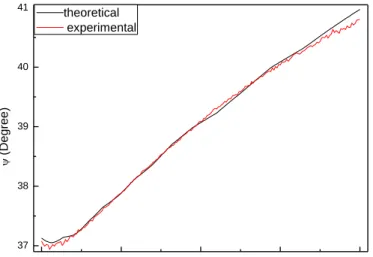
400 500 600 700 800 37,0 37,5 38,0 38,5 39,0 39,5 40,0 40,5 41,0 (D e g re e ) Wavelength (nm) theoretical experimentalFigure 3. 3 :Measured ellipsometric angle ψ as a function of wavelength and simulation for the fit of the model to the data for 25.2 nm thick Ag film on SiO2, sample measured
directly after evaporation.
400 500 600 700 800 37 38 39 40 41 (D e g re e ) Wavelength (nm) theoretical experimental
Figure 3. 4 : Measured ellipsometric ψ as a function of wavelength and simulation for the fit of the model to the data for 25.2 nm thick Ag film on SiO2 measured 7 days after
26
400 500 600 700 800 38,0 38,5 39,0 39,5 (D e g re e ) Wavelength (nm) theoretical experimentalFigure 3. 5 :Measured ellipsometric angle ψ as a function of wavelength and simulation for the fit of the model to the data for 25.2 nm thick Ag film on SiO2 measured 10 days
after evaporation.
The oxide thicknesses with errors of the order of ±0.1 nm for different samples were determined. As an example, the nominal oxide thickness of 18.9 nm thick Ag film on SiO2 after several days is shown in figure 3.6 and 3.7. It can be seen that the oxidation
level of silver in ambient atmosphere is very small and from the sample of thickness 18.9 nm, it can be inferred that the oxidation is self-limited as the oxide thickness does not evolve after a relatively long time.
27
0 2 4 6 8 10 0,2 0,3 0,4 0,5 0,6 0,7 0,8 O xi d e t h ickne ss (n m)Air exposition time (day)
Figure 3. 6 : Oxide thicknesses of the 25.2 nm thick Ag/SiO2 thin film as a function of
air exposition time. The line is drawn to guide the eye.
0 5 10 15 20 25 30 0,65 0,70 0,75 0,80 0,85 0,90 0,95 1,00 1,05 1,10 1,15 O xi d e t h ickne ss (n m)
Air exposition time (day)
Figure 3. 7 : Oxide thicknesses of the 18.9 nm thick Ag/SiO2 thin film as a function of
28
Au thin films
In this case, our ellipsometer model consists of glass at the bottom with Au layer on it. We have determined the thin films thicknesses by fitting our model to the experimental ellipsometric data. An example for actual ellipsometric data and the fit is shown in figure 3.8. In this case, we have not made oxidation analysis for Au samples as Au does not have known native oxide.
400 600 800 1000 1200 24 26 28 30 32 34 36 38 40 (D e g re e ) Wavelength (nm) theoretical experimental
Figure 3. 8 :Measured ellipsometric angle ψ as a function of wavelength and simulation for the fit of the model to the data for 23.8 nm thick Au film on SiO2 sample.
3.2.2. Determination of the optical constants of thin films
We analyzed the ellipsometry data to obtain refractive index (n) and absorption coefficient (k) of different thin film thicknesses. Figure 3.9 and figure 3.10 show the graph of n and k for different thicknesses of Ag/ SiO2, respectively.
29
400 500 600 700 800 0,12 0,13 0,14 0,15 0,16 0,17 0,18 0,19 0,20 0,21 0,22 n Wavelength (nm) Palik 18.8 nm 20.3 nm 25.2 nmFigure 3. 9 :Wavelength dependence of the refractive index (n) of Ag/SiO2 sample for
different Ag film thicknesses (18.8 nm, 20.3 nm and 25.2 nm).
400 500 600 700 800 2,0 2,5 3,0 3,5 4,0 4,5 5,0 k Wavelength (nm) Palik 18.8 nm 20.3 nm 25.2 nm
Figure 3. 10 : Wavelength dependence of extinction coefficient (k) of Ag/SiO2 sample
for different Ag film thicknesses (18.8 nm, 20.3 nm and 25.2 nm).
As seen in the figures, all samples of Ag/SiO2 show similar behavior. They are
30
The same analysis was done for Au/SiO2 samples. The graphics of n and k for different
thicknesses of Au/SiO2 samples are shown in the figures 3.11 and 3.12.
400 600 800 1000 1200 0,0 0,2 0,4 0,6 0,8 1,0 1,2 1,4 1,6 n Wavelength (nm) 14.1 nm 19.2 nm 23.8 nm Palik
Figure 3. 11 : Wavelength dependent refractive index (n) of Au/SiO2 sample for
different Au film thicknesses (14.1 nm, 19.2 nm, 23.8 nm).
400 600 800 1000 1200 2 4 6 8 k Wavelength (nm) 14.1 nm 19.2 nm 23.8 nm (Palik)
Figure 3. 12 :Wavelength dependent extinction coefficient (k) of Au/SiO2 sample for
31
Moreover, the thicknesses of thin films can also be deduced from optical absorbance measurements. Therefore, in the next section, we explain the absorbance properties of Ag and Au thin films.
3.2.3. Absorbance properties of Ag and Au thin films
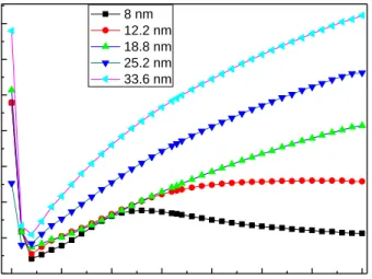
Absorbance measurements can be used as a measure of film thickness. We measured absorbance of all as grown samples. The measurements are shown in the figure 3.13.
300 400 500 600 700 800 900 1000 0,0 0,2 0,4 0,6 0,8 1,0 1,2 1,4 Abso rb a n ce (a .u .) Wavelenght (nm) 8 nm 12.2 nm 18.8 nm 25.2 nm 33.6 nm
Figure 3. 13 :Absorbance of as grown Ag/SiO2 sample for different thicknesses (8 nm,
12.2 nm, 18.8 nm, 25.2 nm, 33.6 nm).
As seen in figure 3.13, absorbance value increases with the film thickness. The 8 nm thick film shows a different behavior from the others. We can see a peak centered around 540 nm. This is due to the plasmonic structure of the film. The sample is composed of nanoscale islands (cf figure 3.17) [29].
Using the dependency of absorbance on film thickness, we can deduce their thicknesses. The absorbance can be described as:
32
where, λ is the wavelength, I0 is the intensity of the incident light and IT is the intensity
of the transmitted light and IT=I0*10-kd where, k and d are the absorption coefficient and
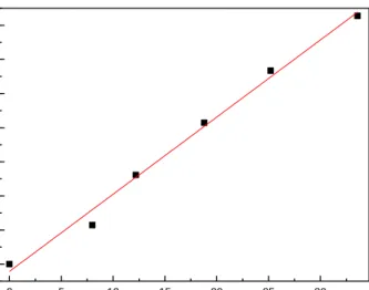
thickness of the sample. As seen in figure 3.14, there is a linear relationship between the absorbance value and the thickness. Very thin films are composed of islands and absorbance shows a different feature due to the effect of plasmon. We observe a wide absorbance peak centered around 540 nm, indicative of the island nature of the thin film. 0 5 10 15 20 25 30 0,0 0,2 0,4 0,6 0,8 1,0 1,2 1,4 Abso rb a n ce @ 1 0 0 0 n m Thickness (nm)
Figure 3. 14 : Absorbance at 1000 nm of as grown Ag/SiO2 samples for different film
thicknesses (8 nm, 12.2 nm, 18.8 nm, 25.2 nm, 33.6 nm).
We also made absorbance measurement for as grown Au/SiO2 samples as presented in
figure 3.15. As in the case of as grown Ag/SiO2 samples, we have determined the
thickness of as grown Au/SiO2 samples. The island growth is also present in the Au thin
films. We note the plasmon related absorbance wide peak around 650 nm and it is consistent with literature [30]. The linear relationship between the absorbance value at 1000 nm and the thickness for Au/SiO2 samples is shown in figure 3.16.
33
400 600 800 1000 0,1 0,2 0,3 0,4 0,5 0,6 0,7 0,8 0,9 1,0 1,1 1,2 Abso rb a n ce (a .u .) Wavelength (nm) 4.1 nm 14.1 nm 19.2 nm 23.8 nmFigure 3. 15 : Absorbance of as grown Au/SiO2 sample for different film thicknesses
(4.1 nm, 14.1 nm, 19.2 nm, 23.8 nm). 0 5 10 15 20 0,0 0,2 0,4 0,6 0,8 1,0 1,2 Abso rb a n ce @ 1 0 0 0 n m Thickness(nm)
Figure 3. 16 : Absorbance at 1000 nm of as grown Au/SiO2 sample for different
34
In addition to the optical constants and the thickness of the films, surface roughness may also play a role in the dewetting. We, therefore, made surface characterization of thin films via AFM.
3.2.4. Surface characterization of thin films
Atomic force microscope (AFM) is used to image and measure surface topography of samples. AFM data provides us with a measure of roughness of the samples. The roughness of a sample can affect the size of the nanoparticles we need to obtain. It is known that as the roughness of the sample increases, the particle size and the length scale obtained after annealing decreases [4]. In this section, we analyze the as grown silver and gold thin films on glass, silicon and fused silica substrates using AFM. In previous sections we showed, through ellipsometer and absorbance measurements the existence of clusters in very thin samples. AFM measurements support these observations. Clusters can be seen in the AFM images of 8 nm thick Ag and 10 nm thick Au on SiO2, and on Si as well as on used silica samples, figure 3.17. Roughness
35
Figure 3. 17 :AFM measurement for 8 nm (a) Ag/SiO2 (b) Ag/Si (c) Ag/fused silica and
for 10 nm (d) Au/SiO2 (e) Au/Si (f) Au/fused silica.
Table 3. 2: AFM measurement
rms roughness of as deposited thin films (nm) 8 nm Ag/SiO2 9.3 8 nm Ag/Si 7.9 8 nm Ag/fused silica 4.6 10 nm Au/SiO2 7.1 10 nm Au/Si 8.4 10 nm Au/fused silica 6.0
36
CHAPTER 4
4.
Nanoparticle formation by cw laser
processing
In this chapter, nanoparticle formation via laser induced dewetting of Ag and Au thin films on different substrates is presented. A cw Ar laser was used to scan the surfaces of thin films at various power densities. Laser processed samples were analysed in terms of particle size, shape and lenght scale as size, shape and lenght scale are dependent on dewetting phenomenon.
4.1. Experimental set up
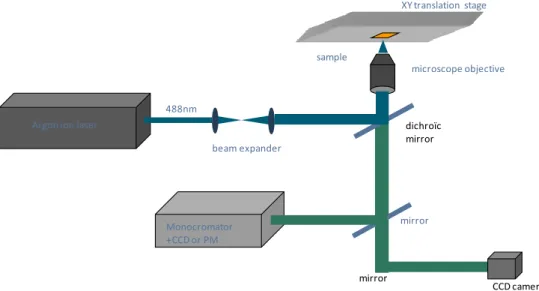
Figure 4.1 presents the experimental set up. In this set-up, a cw Ar+ laser with a number of wavelengths in the UV and visible is used to process the samples. Ar+ laser can also be operated under all lines lasing condition reaching to maximum of 10 W optical power. The sample is mounted on a computer controlled motorized XY translation stage. The laser beam is focused on the sample by a series of microscope objectives. The dwell time can be changed by varying the scan speed of the stage. Different illumination conditions are obtained by using different objectives with various numerical apertures or an added lens with focal length of 25 cm, changing dwell time and the laser power density.
![Figure 2. 4 : Free energy versus film thickness for different phase region [19].](https://thumb-eu.123doks.com/thumbv2/9libnet/5951313.124143/31.892.329.669.253.508/figure-free-energy-versus-thickness-different-phase-region.webp)