1Abstract—In this work, a new CMOS based grounded voltage controlled positive resistor (GVCPR) with one control voltage is proposed. The proposed GVCPR employs only five CMOS transistors, one operated in triode region and others operated in saturation region or OFF. One of the main properties of the proposed GVCPR is its ultra low power consumption; however, a single active component matching condition is needed. A number of SPICE simulation results
using IBM 0.13 μm SIGE013 level-7 CMOS process
parameters such as its performance analysis and verification in tunable voltage-mode first-order all-pass filter and high-Q & high-gain voltage-mode multiple-feedback second-order band-pass filter are included to confirm the theory. The superior performance of the proposed GVCPR is also proven by numeric Figure of Merit calculation.
Index Terms—CMOS, grounded voltage controlled positive resistor, GVCPR, low power dissipation, low voltage circuit, low transistor count circuit, Figure of Merit.
I. INTRODUCTION
Electronically tunable resistors are widely used in analog signal processing. The application of tunable resistors can be found in telecommunications, electronics and measurements such as active RC filters with variable cut-off frequencies, controlled oscillators, variable gain amplifiers, voltage or current dividers, and voltage or current to frequency converters. In VLSI technology, a resistor can be achieved in silicon technology by using poly silicon of diffusion areas [1]. However, resistors of practical values on silicon wafer suffer from limited values and high variability due to process variations. Moreover, its resistance values are not variable, and therefore, they are generally replaced by active resistors [2]. Our detailed literature survey given in Table I shows that during the last three decades several grounded voltage or current controlled positive resistor realizations were
Manuscript received January 1, 2014; accepted May 9, 2014.
Ing. Norbert Herencsar, Ph.D. was supported by the project CZ.1.07/ 2.3.00/30.0039 of Brno University of Technology. Research described in this paper was also in part supported by the project SIX CZ.1.05/2.1.00/03.0072 from the operational program Research and Development for Innovation and Czech Science Foundation projects under No. P102/11/P489 and P102/09/1681.
reported that in standard CMOS technology can be electronically controlled externally via control voltage(s) [3]–[9]. As a main disadvantage of these realizations is high power dissipation. The configurations in [10] and [11] employ respectively four and two bipolar junction transistors (BJTs). However, in practice the BJT-based circuits are less preferred due to their temperature dependence. In [12], the controlled grounded resistor is made up of a junction gate field-effect transistor (JFET) and an active building blocks such as voltage buffer (VB) and second/generation current conveyor (CCII).
In this work, a new CMOS based grounded voltage controlled positive resistor (GVCPR) with one control voltage is proposed. The proposed GVCPR employs only five CMOS transistors, one operated in triode region and others operated in saturation region or OFF. The circuit is supplied by voltages equal to the threshold voltages of the used IBM 0.13 μm SIGE013 level-7 CMOS technology. Hence, one of the main advantages of the proposed GVCPR is its ultra low power consumption. However, the proposed GVCPR needs a single active component matching condition. A number of SPICE simulation results and numerical Figure of Merit calculation are included to confirm the theory and superior performance of the proposed GVCPR.
II. PROPOSEDGROUNDEDVOLTAGECONTROLLEDPOSITIVE RESISTOR
Symbol of the proposed CMOS based GVCPR is given in Fig. 1 where –VTPand –VTNare positive and negative power supply voltages, respectively. Also, Vcis control voltage of the proposed CMOS based GVCPR. Apart from these, VTP and VTN are respectively threshold voltages of PMOS and NMOS transistors [13]. From Fig. 1, impedance of the proposed GVCPR is defined as follows
( ). in in eq c in V Z R f V I (1)
In fact, the equivalent input resistance of the GVCPR is a function of the control voltage Vc.
Grounded Voltage Controlled Positive Resistor
with Ultra Low Power Consumption
E. Yuce
1, S. Minaei
2, N. Herencsar
31
Department of Electrical and Electronics Engineering, Pamukkale University,
Denizli, Kinikli-20070, Turkey
2
Department of Electronics and Communications Engineering, Dogus University,
Acibadem, Kadikoy 34722, Istanbul, Turkey
3
Department of Telecommunications, Brno University of Technology,
Technicka 3082/12, 616 00 Brno, Czech Republic
ELEKTRONIKA IR ELEKTROTECHNIKA,ISSN1392-1215,VOL.20,NO.7,2014
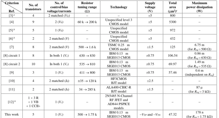
TABLE I. COMPARISON OF PREVIOUSLY PUBLISHED GROUNDED VOLTAGE OR CURRENT CONTROLLED POSITIVE RESISTORS.
Criterion Ref. No. of transistors No. of control/bias voltage/currents Resistor tuning range () Technology Supply voltage (V) Total area (m2)c Maximum power dissipation (W) [3]a 4 2 matched (V G) ±5 800 [4] 9 2 (Vb) 60 k 200 k Unspecified level 3 CMOS model ±5 5300 [5]b 5 1 (Vb) Unspecified CMOS model ±5 972 [6]b 2 2 matched (V) Unspecified CMOS model ±5 432 [7] 8 2 matched (V) 500 1.6 k TSMC 0.25 μm CMOS model ±1.5 125 6.75 m (for Req= 500)
[8] circuit 1 8 In both 1 (Vc) 630 830 IBM 0.13 μm
SIGE013 CMOS ±0.75 106.54
0.86 m (for Req= 630)
[8] circuit 2 10 In both 1 (Vc) 535 810 IBM 0.13 μm
SIGE013 CMOS ±0.75 69.97 1.49 m (for Req= 535) [9] 3 1 (Vc) 411 800 IBM 0.13 μm SIGE013 CMOS ±0.75 57.46 0.6 m (independent on Req) [10] 4 2 matched (I0) 35 120 k HF3CMOS BJT model ±2.5
[11] 2 2 matched (I0) 34 285 k ALA400-CBIC-RBJT model ±1.5 87
(for Req= 3 k) [12]b 1 + 3 R + 1 VB + 1 CCII+ 1 (Vc) 2N5485 N-Channel RF JFET and AD844 PSPICE models
This work 5 1 (Vc) 500 1.75 k IBM 0.13 μm
SIGE013 CMOS VTPandVTN 47.32
178 n (for Req= 1.75 k)
Notes: “–“ – not mentioned; “a“ – simulations are not provided; “b“ – Obtained simulation results are not commented; “c“ – Sum of products of the widths and lengths of each
transistors in the CMOS resistors.
Fig. 1. Symbol of the proposed grounded voltage controlled positive resistor.
Fig. 2. Proposed CMOS GVCPR dissipating very low power.
The proposed CMOS GVCPR is depicted in Fig. 2. The transistor M2is operated in linear region (VGS2– VTN2> VDS2 = │Vin│), which has the following drain current, iD2, for all
Vin
2 2 2 2 , 2 in D N c TN in V i k V V V (2)where kN2 is the transconductance parameter of the M2
transistor and VTN2is the threshold voltage with body effect [13]. For the proposed GVCPR in Fig. 2, it is assumed that all the transconductance parameters are equal. In other words, kP1= kN2= kN3= kN4= kN5= k. Routine analysis of the proposed GVCPR in Fig. 2, the following input current is found
2 3 4.
in D D D
I i i i (3)
For Vin> 0, M2and M3are ON while M1, M4and M5are
OFF thus the following drain currents are obtained
2 3 2 , D in k i V (4) and 4 0. D i (5)
For Vin< 0, M3is OFF while M1, M2,M4and M5are ON
thus the following drain currents are obtained
3 0 , D i (6) and 2 4 2 . D in k i V (7)
After combining equations from (3) to (7), the following input resistance is evaluated
2 1 . ( ) in eq in c TN V R I k V V (8)
It is important to note that one should select Vc> VTN2in addition to VGS2– VTN2> │Vin│ for proper operation of the proposed GVCPR.
III. SIMULATIONRESULTS
To verify the theoretical study, the behavior of the proposed GVCPR shown in Fig. 2 has been verified by SPICE simulations. In the design, transistors are modeled by
ELEKTRONIKA IR ELEKTROTECHNIKA,ISSN1392-1215,VOL.20,NO.7,2014
the IBM 0.13 μm SIGE013 level-7 CMOS process parameters (VTN= 0.0408721 V, N= 451.7567843 cm2/(Vs), V
TP=0.2178731 V, P= 100 cm2/(Vs),
TOX= 3.2 nm) [14]. The aspect ratios of all the NMOS (M2–
M5) and PMOS (M1) transistors in Fig. 2 are chosen as
6.5m/1.04 m and 19.5 m/1.04 m, respectively. In the GVCPR, a DC voltage equal to Vb= –0.75 V is connected to the bulk of the transistor M2, while the bulk of other
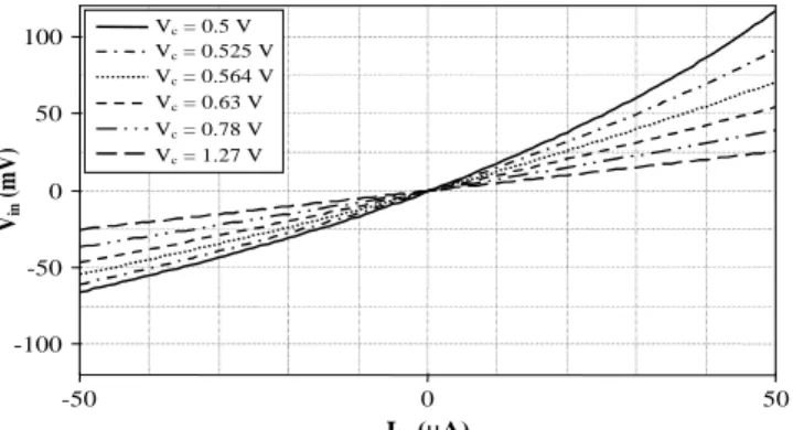
transistors are connected to their corresponding sources to prevent body effect. The –0.75 V voltage is standard voltage (VSS) of the used IBM 0.13 μm SIGE013 CMOS technology and can be easily found in a system that is realized with technology. Iin (A) -50 0 50 -100 -50 0 50 100 Vin ( m V ) Vc = 0.564 V Vc = 0.63 V Vc = 0.525 V Vc = 0.5 V Vc = 0.78 V Vc = 1.27 V
Fig. 3. I – V characteristics of the proposed GVCPR for different values of control voltage Vc.
First of all, the performance of the GVCPR was tested by DC analysis. The I – V characteristics are shown in Fig. 3, that were performed by applying input currents to resistor and obtaining the corresponding voltages on the same terminal. The proposed circuit was varied by control voltage values Vc= {0.5; 0.525; 0.564; 0.63; 0.78; 1.27} V and it behaves as a resistor with equivalent values of Reqbetween 1.75 k to 500 by 250 decrement. Similarly, the value of Reqversus control voltage Vc is depicted in Fig. 4. It can be again seen that the obtained resistance changes from 1.75 k to 500 by varying Vc from 0.5 V to 1.3 V by 10 mV increment. 0.4 0.6 0.8 1.0 1.2 1.4 0 0.5 1.0 1.5 2.0 Control voltage Vc (V) Req ( k )
Fig. 4. Controllability of the Reqwith respect to the control voltage Vc.
Figure 5 illustrates the time-domain performance of the GVCPR with value equal to Req 1 k (Vc= 0.63 V), in which transient analysis was applied from 100 ns to 200 ns by 50 ps step sizes for sinusoidal input currents at
f = 100 MHz and three different magnitudes Iin= {15; 30;
45} μA. Fast Fourier Transform (FFT) characteristics of the
GVCPR are given in Fig. 6 while keeping the same settings.
Time (ns) 100 110 120 130 -45 0 45 -45 0 45 Vin ( m V ) Iin ( A ) Iin = 45A
Iin = 15A Iin = 30A Iin = 45A
Time (ns) 100 110 120 130 (a) Time (ns) 100 110 120 130 -45 0 45 -45 0 45 Vin ( m V ) Iin ( A ) Iin = 30A Iin = 45A
Iin = 15A Iin = 30A Iin = 45A
Time (ns)
100 110 120 130
(b)
Fig. 5. Time-domain responses of the proposed GVCPR for Req 1 k:
(a) applying sinusoidal input currents with f = 100 MHz and three different magnitudes, (b) voltage responses.
Iin = 15A Iin = 30A Iin = 45A Frequency (GHz) 0 0.2 0.4 0.6 0.8 1.0 100n 10 1m 100m Vin ( V )
Fig. 6. FFT responses for the proposed GVCPR for Req 1 k applying
sinusoidal input currents with f = 100 MHz and different magnitudes.
Iin (A) 0 20 40 60 80 100 0 2 4 6 8 T H D ( % ) Req = 1 k Req = 750 Req = 500
Fig. 7. Distortion characteristics of the proposed GVCPR for three different values of Reqagainst applied input currents at f = 100 MHz.
In Fig. 7, distortion characteristics of the GVCPR for
Vc= {0.63; 0.78; 1.27} V (Req 1 k, 750 , 500 ) are depicted, where sinusoidal input currents with f = 100 MHz and different magnitudes are applied to the circuit separately to find out total harmonic distortion (THD) of the corresponding voltages on the same terminal. For Req 1 k it can be seen that an input with amplitude of 50A yields THD value of 3.87%.
ELEKTRONIKA IR ELEKTROTECHNIKA,ISSN1392-1215,VOL.20,NO.7,2014 45 60 15 75 -90 -45 0 30 Frequency (Hz) 100 1k 10k 100k 1M 10M 100M 1G 10G 100G |R e q | (dB ) Phase (de g.) Vc = 0.564 V Vc = 0.63 V Vc = 0.525 V Vc = 0.5 V Vc = 0.78 V Vc = 1.27 V Frequency (Hz) 100 1k 10k 100k 1M 10M 100M 1G 10G 100G (a) 45 60 15 75 -90 -45 0 30 Frequency (Hz) 100 1k 10k 100k 1M 10M 100M 1G 10G 100G |R e q | (dB ) Phase (de g.) Vc = 0.564 V Vc = 0.63 V Vc = 0.525 V Vc = 0.5 V Vc = 0.78 V Vc = 1.27 V Frequency (Hz) 100 1k 10k 100k 1M 10M 100M 1G 10G 100G (b)
Fig. 8. Phase and magnitude responses of the proposed GVCPR with respect to frequency where control voltage Vcvaries between 0.5 V and
1.27 V.
In Fig. 8, for different values of Vc, the frequency responses of the phase and magnitude of
Req 1.75 k 500 by 250 decrement are shown, obtained from AC analysis. It can be seen that the phase difference between Iin and Vin for the proposed circuit is nearly zero from very low frequencies to 10 MHz. Moreover, the magnitude of the Req is approximately constant up to 100 MHz. Using the ONOISE statement, the output noise behavior for three different values of
Req {1.5 k; 1 k; 500 } with respect to frequency have also been simulated, as it is shown in Fig. 9. The most important feature of the proposed GVCPR is its ultralow power consumption due to the very low biasing current.
0.1 1 10 Frequency (Hz) 100 1k 10k 100k 1M 10M 100M 1G 10G 100G Voltage n oise (n V/ Hz) Req = 1.5 k Req = 1 k Req = 500
Fig. 9. Output voltage noise variation of the proposed GVCPR for three different values of Reqversus frequency.
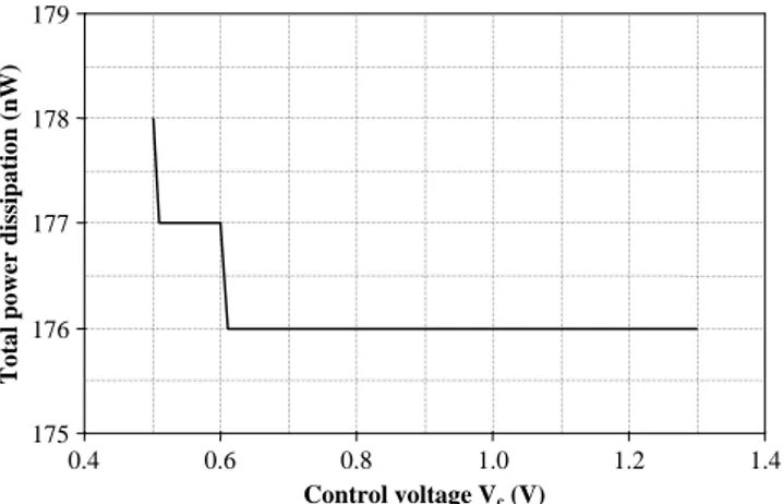
The power consumption versus applied various control
voltages for the proposed GVCPR is shown in Fig. 10, where the Vcis increased from 0.5 V to 1.3 V by 10 mV step size. 0.4 0.6 0.8 1.0 1.2 1.4 175 176 177 178 179 Control voltage Vc (V) T o ta l p o w er d is sip a tio n (n W )
Fig. 10. Total power dissipation of the proposed GVCPR versus control voltage Vc.
From the simulation results, it can be seen that the proposed resistor consumes ultralow power (around 176 nW) and the results are in good agreement with the theory.
IV. APPLICATIONEXAMPLES
In this section, the performance of the proposed GVCPR in Fig. 2 is tested in more complex circuits such as in tunable voltage-mode (VM) first-order all-pass filter (APF) and high-Q and high-gain VM multiple-feedback (MFB) second-order band-pass (BP) filter.
A. Tunable VM First-Order All-Pass Filter
First of all, to demonstrate the usefulness of the proposed GVCPR, it was used in VM first-order APF, which is shown in Fig. 11 [15].
Fig. 11. VM first-order all-pass filter example for testing the proposed GVCPR [15].
An APF (phase shifter) is a useful analog signal processing unit, which finds wide application areas in control or measurement systems in order to shift phases of the signals while keeping their amplitudes unchanged. Assuming R1= R2, routine analysis yields the following
voltage transfer function (TF) for the circuit in Fig. 11
1, 1 eq out in eq sCR V T s V sCR (9)
180 2 tan 1
.eq
CR
(10)
The pole frequency of the VM first-order APF is calculated as 0 1 . 2 eq f CR (11)
Hence, the proposed GVCPR can be with advantage used for tuning the f0of the filter via control voltage Vc.
In order to confirm the performance of the proposed GVCPR, the behavior of the VM first-order APF shown in Fig. 11 has also been verified using SPICE software. In simulations the passive element values were chosen as
R1= R2= 1 kΩ, C = 53 pF, and the ADA4899-1 [16]
ultralow noise and distortion unity-gain stable high speed voltage feedback op amp was used with DC power supply voltages equal to ±5 V. Fig. 12 shows the ideal and simulated gain and phase responses illustrating the electronic tunability of the filter example. The pole frequency is varied for f0 {1.9; 3; 4; 5.8} MHz via control voltage Vc= {0.5; 0.63; 0.78; 1.27} V of the proposed GVCPR, respectively. Similarly, possibility of tuning the pole frequency f0via Vcis shown in Fig. 13, where the control voltage was increase from 0.5 V to 1.27 V by 10 mV step size.
Frequency (Hz) 1k 10k 100k 1M 10M 100M -4 -2 0 2 4 0 45 90 135 180 Vc = 0.78 V Vc = 1.27 V Vc = 0.63 V Vc = 0.5 V P h a se (d eg .) G a in ( d B )
Fig. 12. Electronical tunability of the pole frequency of the VM first-order all-pass filter by the proposed GVCPR.
0.4 0.6 0.8 1.0 1.2 1.4 0 2 4 6 8 Control voltage Vc (V) f0 (M H z)
Fig. 13. Tuning the pole frequency of the VM first-order all-pass filter via control voltage Vcof the proposed GVCPR.
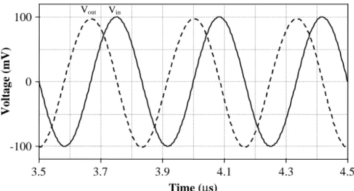
Finally, to illustrate the time-domain performance, transient analysis was performed to evaluate the voltage
swing capability and phase errors of the filter as it is demonstrated in Fig. 14. A sine-wave input of 100 mV amplitude and frequency of 3 MHz was applied to the filter while keeping the passive element values as listed above and setting Vc= 0.63 V (Req 1 kΩ). Note that the output waveform is in 90 degree phase shift with the input one. The total harmonic distortion (THD) at this frequency is found as 3.48 %. Time (s) 3.5 3.7 3.9 4.1 4.3 4.5 -100 0 100 Vout Vin V o lt a g e (m V )
Fig. 14. Time-domain responses of the VM first-order all-pass filter at 3 MHz.
B. High-Q and High-Gain VM MFB Second-Order Band-Pass Filter
As a second test, the proposed GVCPR is used in high-Q and high-gain VM infinite-gain MFB second-order BP filter, which is given in Fig. 15 [12]. Routine circuit analysis yields the following VM TF for the circuit
2 2 1 BP 2 1 2 2 1 2 , 1 p out in p p R R sC V R H V s C C R R s C C R (12) where Rp= R1 Req.The natural angular frequency 0, quality factor Q, and
centre frequency gain H0 can be derived from (12) as
follows: 0 1 2 2 1 , p = C C R R (13)
2 1 2 1 2 , p R C C Q R C C (14)
2 2 0 1 1 2 . R C H R C C (15)In SPICE simulations again the ADA4899-1 [16] ultralow noise and distortion unity-gain stable high speed voltage feedback op amp was used with DC power supply voltages equal to ±5 V and passive component values were chosen as
C1= C2= 20 pF, R1= 1 kΩ, and R2= 120 kΩ.
To demonstrate the utility of the proposed GVCPR, its value in the filter given in Fig. 15 was changed via control voltage Vc= {0.5; 0.63; 0.78; 1.27} V and magnitude responses are depicted in Fig. 16. It can be seen that as Vc increases (Req decreases), 0 and Q increase, which is
ELEKTRONIKA IR ELEKTROTECHNIKA,ISSN1392-1215,VOL.20,NO.7,2014
Fig. 15. High-Q and high-gain VM infinite-gain MFB second-order BP filter example for testing the proposed GVCPR [12].
10k 100k 1M 10M 100M -20 0 20 40 Frequency (Hz) M a g n it u d e (d B ) Vc = 0.78 V Vc = 1.27 V Vc = 0.63 V Vc = 0.5 V
Fig. 16. Electronically tuned high-Q and high-gain BP filter magnitude responses.
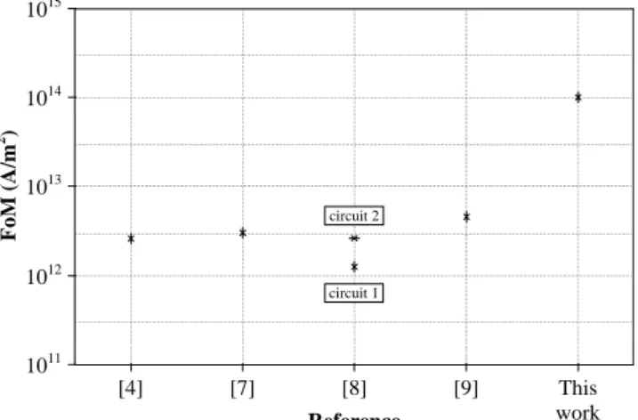
V. FIGURE OFMERIT
In order to provide additional evaluation and fair comparison of proposed GVCPRs in literature, a numeric Figure of Merit (FoM) was calculated by
2
,
resistor tuning range A
FoM
supply voltage total area m
(16)
where the related values were taken from Table I and the results are depicted in Fig. 17. Note that due to limited information in some of the listed references the FoM is calculated and compared only for GVCPRs in [4] and [7]– [9]. Here it is worth noting that for the proposed GVCPR the highest value of FoM denotes superior circuit performance.
[4] [7] [8] [9] This work Reference circuit 2 circuit 1 1011 1012 1013 1014 1015 F o M (A /m 2 )
Fig. 17. Performance comparison of grounded voltage controlled positive resistors listed in Table I.
VI. CONCLUSIONS
In this study, a new CMOS based GVCPR with one control voltage is proposed. The proposed GVCPR employs only five CMOS transistors, one operated in triode region and others operated in saturation region or OFF. One of the main properties of the proposed GVCPR is its ultra low power dissipation. Nevertheless, the proposed GVCPR requires a single active component matching constraint. A number of SPICE simulation results verify the claimed theory well as expected.
REFERENCES
[1] D. A. Johns, K. Martin, Analog Integrated Circuit Design. New York: John Wiley & Sons, 1997, pp. 112–115.
[2] S. A. Tekin, M. Alci, “Design and applications of electronically tunable floating resistor using differential amplifier”, Elektronika ir Elektrotechnika, vol. 19, no. 4, pp. 41–46, 2013. [Online]. Available: http://dx.doi.org/10.5755/j01.eee.19.4.1310
[3] C.-S. Park, R. Schaumann, “A high-frequency CMOS linear transconductance element”, IEEE Trans. on Circuits and Systems, vol. CAS-33, no. 11, pp. 1132–1138, 1986. [Online]. Available: http://dx.doi.org/10.1109/TCS.1986.1085859
[4] G. Wilson, P. K. Chan, “Novel voltage-controlled grounded resistor”, Electronics Letters, vol. 25, no. 25, pp. 1725–1726, 1989. [Online]. Available: http://dx.doi.org/10.1049/el:19891154
[5] Z. Wang, “Novel voltage-controlled grounded resistor”, Electronics Letters, vol. 26, no. 20, pp. 1711–1712, 1990. [Online]. Available: http://dx.doi.org/10.1049/el:19901093
[6] Z. Wang, “2-MOSFET transresistor with extremely low distortion for output reaching supply voltages”, Electronics Letters, vol. 26, no. 13, pp. 951–952, 1990. [Online]. Available: http://dx.doi.org/10.1049/ el:19900620
[7] E. Yuce, S. Minaei, H. Alpaslan, “Novel CMOS technology-based linear grounded voltage controlled resistor”, Journal of Circuits, Systems, and Computers (JCSC), vol. 20, no. 3, pp. 447–455, 2011. [Online]. Available: http://dx.doi.org/10.1142/S0218126611007384 [8] E. Yuce, S. Minaei, H. Alpaslan, “Single voltage controlled CMOS
grounded resistors and their application to video filter”, Indian Journal of Engineering and Material Sciences. (submitted for publication in 2013).
[9] E. Yuce, S. Tokat, F. Yucel, “A new wideband electronically tunable grounded resistor employing only three MOS transistors”, Turk. J. Elec. Eng. & Comp. Sci., 2014.
[10] O. Saaid, A. Fabre, “Class AB current-controlled resistor for high performance current-mode applications”, Electronics Letters, vol. 32, no. 1, pp. 4–5, 1996. [Online]. Available: http://dx.doi.org/10.1049/ el:19960023
[11] R. Arslanalp, E. Yuce, A. T. Tola, “Low component count BJT technology based current controlled tunable resistors and their applications”, IET Circuits, Devices and Systems, vol. 7, no. 1, pp. 21–30, 2013. [Online]. Available: http://dx.doi.org/10.1049/iet-cds.2012.0214
[12] B. Maundy, S. Gift, P. Aronhime, “Practical voltage/current-controlled grounded resistor with dynamic range extension”, IET Circuits, Devices & Systems, vol. 2, no. 2, pp. 201–206, 2008. [Online]. Available: http://dx.doi.org/10.1049/iet-cds:20070164 [13] B. Razavi, Fundamentals of Microelectronics, 2008.
[14] IBM 0.13 μm SIGE013 level-7 CMOS technology SPICE models. [Online]. Available on http://www.mosis.com/cgi-bin/cgiwrap/ umosis/swp/params/ibm-013/t97f_8hp_5lm-params.txt
[15] R. Genin, “Realization of an all-pass transfer function using operational amplifiers”, in Proc. IEEE, vol. 56, no. 10, pp. 1746– 1747, 1968. [Online]. Available: http://dx.doi.org/10.1109/ PROC.1968.6731
[16] Datasheet ADA4899-1 – Unity-Gain Stable, Ultralow Distortion, 1 nV/√Hz Voltage Noise, High Speed Op Amp. Analog Devices, Rev. B, 6/2007.