Temperature-dependent C-V characteristics of Au/ZnO/n-Si
device obtained by atomic layer deposition technique
A. Kocyigit1 · I. Orak2,3 · Ş. Aydoğan4 · Z. Çaldıran4 · A. Turut5
Received: 4 October 2016 / Accepted: 19 December 2016 © Springer Science+Business Media New York 2017
free charges in the interface. The series resistance (Rs) of
the device was taken into account to understand its effect on main electrical parameters, and it could be seen from these results that the Rs strongly depends on the device
tem-perature. The impedance (Z) values decreased with chang-ing from −1 to +2 V bias voltages and increaschang-ing tempera-ture. The barrier height which was obtained from the C−2-V
plots increased a slope of 0.00108 eV/K with a decrease in temperature from 160 to 340 K. It can be concluded that the Au/ZnO/n-Si device may be used and improved for next technological applications such as capacitor and memristor.
1 Introduction
There is a great interest in metal–semiconductor devices in the electronic industry owing to their versatile techno-logical applications [1–5]. Sometimes, metal oxide (ZnO, SnO2,…) and insulator layers insert between the metal
and semiconductor in order to control properties of these devices [6]. These properties contain diode parameters such as barrier height, ideality factor and interface states. There are many using areas of these devices such as rectifi-ers [7], inverters [8], polarity protection [9] and freewheel-ing diodes [10].
The ZnO has a high direct band gap of 3.37 eV, large exciton binding energy (60 meV) and very promising prop-erties, such as the combination of low costs, non-toxicity and low temperature deposition [11, 12]. The semiconduc-tor ZnO has also many using areas in electronic industry such as chemical sensors [13], varistors [14], solar cells [15], UV photo detectors [16], lasers [17] and light-emit-ting diodes [18]. It could be numbered many techniques to obtain the ZnO layers between the metal and semiconduc-tor such as spray pyrolysis [19], spin coating [20], atomic
Abstract Since the importance of Schottkky devices, Au/
ZnO/n-Si device were obtained, and the capacitance–volt-age (C-V) and conductance-voltcapacitance–volt-age (G-V) characteristics of Au/ZnO/n-Si device were studied using admittance spectroscopy at changing temperature from 160 to 340 K with 20 K intervals and −1 to +2 V bias voltage range. The interface thin film ZnO layer was deposited on the n-type Si wafer by atomic layer deposition technique (ALD) in order to obtain homogenous interface layer. The layer thick-ness of ZnO was taken as 10 nm by the resulting ZnO film growth rate at about 1.45 Å per cycle. This thin film layer was characterized with XRD and AFM analyses. It can be seen from the C-V curves of the device that the capacitance values increased in depletion region with increasing tem-perature and exhibited peaks towards to forward biases after 240 K temperature. The changing of capacitance values confirmed re-ordering and re-structuring of charges in the interface of the device with changing temperature. The G-V curves of the device also increased with increasing temper-ature and towards to forward bias voltages due to increasing
* A. Kocyigit
1 Department of Electrical Electronics Engineering, Engineering Faculty, Igdir University, 76000 Igdir, Turkey 2 Vocational School of Health Services, Bingöl University,
12000 Bingöl, Turkey
3 Department of Physics, Faculty of Sciences and Arts, Bingöl University, 12000 Bingöl, Turkey
4 Department of Physics, Faculty of Sciences, Ataturk University, 25100 Erzurum, Turkey
5 Engineering Physics Department, Faculty of Engineering and Natural Sciences, Istanbul Medeniyet University, 34700 Istanbul, Turkey
layer deposition (ALD) [21]. Among these technique, the ALD has significant advantages because it has large area uniformity, definite thickness control, highly protective deposition, and ALD technique can be used under low tem-perature growth which is very important for the fabrication of low cost and flexible electronics [22].
To better understand the properties of metal–semicon-ductor devices, it should be obtained temperature depend-ent electrical characteristic of these devices. On the other hand, temperature dependent electrical characterizations provide more information about conduction mechanism, interface states and barrier inhomogeneity of metal–semi-conductor devices [23–26]. If the literature is investigated, it could be seen many studies about temperature depend-ent electrical characterization of differdepend-ent metal–semicon-ductor structures because of its importance. For example, Kumar et al. [27] investigated TiO2/Si MOS device at dif-ferent annealing temperature, and they found that electrical parameters were influenced changing temperature. Weich-sel et al. [28] studied temperature dependent capacitance effects on palladium zinc oxide Schottky structure, and they obtained changing capacitance and diode parameters with changing temperature. Reddy et al. [29] researched the temperature-dependent current–voltage (I-V) and capaci-tance–voltage (C-V) characteristics of Pt/Ti/n-InP Schottky structures. There are no so many investigations about the temperature-dependent C-V characteristics of Au/ZnO/n-Si devices in the literature.
In addition to above properties of Schottky devices, if a metal dopes on semiconductor surface, the obtained metal semiconductor devices exhibit a capacitor like behavior depending on frequency [30]. In this context, the aims of this study are to investigate the capacitor properties of the Au/ZnO/n-Si device at different temperatures from 160 to 340 K as step 20 K using impedance spectroscopy for tech-nological applications and to fill the literature about tem-perature dependent electrical properties of Au/ZnO/n-Si device.
2 Materials and methods
n-type Si wafer, which had (100) orientation and 7.3 × 1015 cm−3 carrier concentration with respect to
manufacturer specifications, was used for the fabrica-tion of the ZnO/n-Si heterojuncfabrica-tion. The n-type Si wafer was cut into pieces of 1.0 cm length and 1.0 cm breadth. Before using this wafer, it was polished and cleaned with various solvents, and then it was degreased consecutively in acetone and methanol for 3 min. After cleaning, the wafer was etched with H2SO4:H2O2:H2O (5:1:1) for 1 min
to remove the surface damages and undesirable impuri-ties. Gold was evaporated (thermal) on the back side of
the wafer for ohmic contact, and the n-Si/Au structure was annealed at 450 °C for 3 min in N2 atmosphere. The
thickness of metal coverage was determined using a quartz thickness monitor placed in close proximity to the Si sample. The ZnO layer was deposited on n-Si wafer with ALD technique as 10 nm thickness with 1.45 Å growth rate at per cycle. Au metal was evaporated on the ZnO surface as metallic contacts using mask which had 1.0 mm diameter holes on it. The device was character-ized with C-V measurements in the range of 160–340 K temperatures with 20 K intervals at 500 kHz frequency by using a homemade liquid nitrogen cryostat equipped with a temperature controller in darkness. The ZnO film layer in the device was also characterized with Bruker D8 Discover XRD and PSIA XE-100E model AFM.
3 Result and discussion
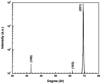
XRD patterns of the ZnO film have been shown in Fig. 1. According to this figure, only ZnO peaks can be seen from XRD pattern; (100), (103) and (201) peaks. The XRD pattern of the ZnO has indicated that the ZnO thin film was deposited successfully using by ALD technique on n-Si wafer surface.
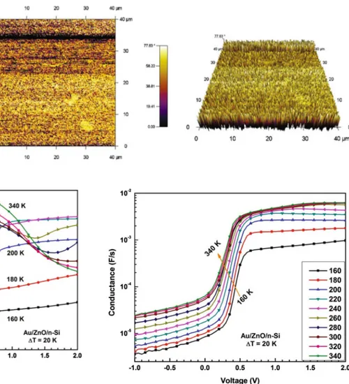
2D and 3D AFM images of the ZnO thin film have been indicated in Fig. 2 for 40 μm x 40 μm wide area scanning. It can be seen from the AFM images that the ZnO surface has good homogeneity and smoothness. It can be said from this figures that ALD technique is very effective for smooth ZnO thin film layer.
Figure 3 has shown the C-V characteristics of Au/ ZnO/n-Si device at changing temperatures from160 K to
340 K and bias voltage from −1 to +2 V at 500 kHz fre-quency. It can be seen from this figure that the tempera-ture and applied bias voltage strongly have affected the capacitance behavior of the Au/ZnO/n-Si device. In the inversion region of the C-V characteristics, capacitance values almost have not influenced from temperature, but they have increased suddenly in depletion region due to narrowing depletion region with increasing forward bias and increasing temperature. The capacitance graphs have exhibited peaks above 240 K temperatures, and the peak positions have changed towards to negative biases. These peaks and changing at their positions could be ascribed to reordering of the near midgap interface states and series resistance with changing temperature [31–35].
In addition, the increasing capacitances and intensity of peaks can be attributed to changing freeze-out effect in charges with increasing temperature [36–38]. The high capacitance values near room temperature imply that the device may be used at room temperature for capacitor and memristor applications [39, 40].
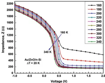
The G-V plots of the Au/ZnO/n-Si device at various tem-peratures for 500 kHz frequency have been shown in Fig. 4. It can be said from this figure that the conductance values have been influenced also from applied forward biases and increasing temperatures [40]. Increasing forward bias from zero to 0.5 V value, the conductance values have increased suddenly. These increasing can be attributed to narrowing depletion region and charges which have enough energy to escape from traps in the interface [32]. The changing tem-perature from 160 K to 340 K, the conductance values have increased depending on increasing mobility of charge car-ries and decreasing secar-ries resistance of the device [41].
It should be also investigated the series resistance (Rs)
of the device to more understand the device properties. The series resistance can cause a serious error in the extraction of interfacial properties and doping profiles from admit-tance measurements, and it can limit the sensitivity of the small-signal steady-state methods. Therefore, it is not pos-sible series resistance to be neglected. The series resistance
Fig. 2 AFM images of the ZnO
layer surface onto n-Si substrate
Fig. 3 (online color) C-V characteristics of Au/ZnO/n-Si device at
various temperature and 500 kHz Fig. 4 (online color) G-V characteristics of Au/ZnO/n-Si device with
equation is given by following formula depending conduct-ance and capacitconduct-ance values:
where Gmand Cm are measured conductance and
capaci-tance, respectively, and 𝜔 is angular frequency and equal to 2𝜋f. Rs values were calculated from Eq. (1) using the
meas-ured conductance and capacitance values for each tempera-ture in Figs. 1 and 2. Then, the series resistance–voltage
(R–V) curves of the Au/ZnO/n-Si device in the temperature
range of 160–340 K have been indicated in Fig. 5.
As can be seen from Fig. 5, the Rs values have
remained almost unchanged in the reverse bias region (negative voltages) and at high voltages in the forward bias region (positive voltages) for each temperature. Fur-thermore, it can be seen that the observed series resist-ance peaks in the forward bias region have shifted from about 0.60 V at 160 K to 0.25 V at 300 K. The peak posi-tion of the series resistance has increased very slightly towards to negative voltage with increasing temperature. When the interface state density in equilibrium with the semiconductor becomes lower than expected one, the series resistance effect is more obvious. Therefore, it can be said that the interface state density is lower in this voltage range. The interface states in this voltage range are called the near midgap states. These kinds of results can be seen in the literature. For example, D.A. Jameel et al. [42] fabricated PANI/(100) GaAs and PANI/ (311)B GaAs devices by a simple technique to fabricate hybrid devices, where polyaniline thin films was called PANI. They [42] observed two peaks for the temperature-dependent series resistance–voltage curves of the PANI/
Rs= Gm G2 m+ ( 𝜔Cm)2
(100) GaAs. One of the peaks appeared in the reverse bias region and the other in the forward bias region, and one peak in only forward bias region for the PANI/(311)B GaAs device for each temperature. The series resistance value for both devices increased with decreasing temper-ature in the reverse and forward bias regions. Yakupha-noglu [43] obtained the series resistance–voltage curves from C-V and G-V characteristics of the Al/p-Si/n-CdO diode under various frequencies at 300 K. He observed two peaks 0.0–1.0 V range in forward bias region of the
series resistance–voltage curves. This behavior had been
attributed to the changes and distribution density of inter-face states [35, 44].
Figure 6 shows impedance-voltage (Z-V) curves of Au/ ZnO/n-Si device in changing temperature from 160 K to 340 K at 500 kHz frequency. According to this figure, the impedance values generally have decreased with increas-ing temperature in a given voltage. This decreasincreas-ing can be attributed to freezing effect which is eliminated with increasing temperature, and charges need less energy to run away from traps at high temperatures [37, 45]. On the other hand, this case may be ascribed to the contributions of majority carriers and interface states to the conductiv-ity [29, 41]. In addition, the Z values have decreased with changing bias voltage from −1 V to about 0.5 V (deple-tion region), and then they have remained constant in the accumulation region. Also, these changing in the Z val-ues with temperature and voltage prove particular distri-bution of interface states or presence of interfacial layer ZnO effect [40, 41].
The C− 2-V plots of the Au/ZnO/n-Si device
depend-ing on temperature have been shown in Fig. 7. It can be seen from this figure that these plots are linear and almost
Fig. 5 (online color) Series resistance–Voltage (R-V) curvess of Au/
parallel each other which indicates uniform dopant con-centration and ideal rectifying contact of the device [36,
45, 46]. Also, it can be said from these plots that charges cannot follow ac signal in the depletion region [45]. Fur-thermore, V0 intercept potentials (Table 1), which was
obtained from the C−2-V plots, have decreased almost
periodically with increasing temperature. These changing can be ascribed to interface states of the device [47].
By using C−2-V graphs, Fermi energy level (E
F), barrier
height (Φb), maximum electric field (Em), concentration
donor atoms (Nd) and effective density of conduction band
(Nc) were calculated, and the values of these parameters
were tabulated in Table 1. EF values have increased with
increasing temperature due to increasing charge carriers in the interface of device or increasing donor concentrations [32, 45, 47]. Em values have decreased with increasing
tem-perature owing to the increasing charge carriers.
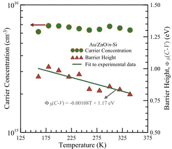
It could be seen from Fig. 8 that the barrier heights and donor concentrations of device have changed depending
on temperature. The barrier heights have decreased a slope of 0.00108 eV/K with an increase in temperature from 160 to 340 K. This decrasing can be ascribed that increasing temperature has caused the decrease the band gap of Au/ZnO/n-Si device [32, 40, 45]. However, donor concentration plot has some fluctuations, but it gener-ally has not so changed with increaing temperature (in Table 1). This case may be compared with some results in the literature [25, 45].
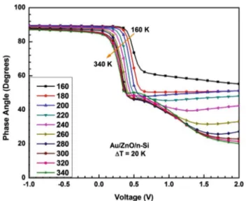
Phase angle (θ) versus voltage graphs of the device have been shown in Fig. 9 for changing temperatures from 160 to 340 K. Phase angel values have not changed from −1 V to about 0.25 V, but they have decreased with increasing temperature after 0.25 V. It can be said from this results that device is more capacitive in the forward biases rather than reverse biases because phase angel val-ues have remained constant at 90° at reverse biases [48].
Fig. 7 (online color) C−2-V plots of Au/ZnO/n-Si device changing temperature from 160 K to 340 K
Table 1 The some electrical
parameters of Au/ZnO/n-Si device obtained C− 2-V graphs
T(K) Nd (1015 cm− 3) Nc (1017 cm− 3) EF (eV) eV0 (eV) Φb (eV) Em (104 V/m)
160 6.16 1.70 0.046 0.90 0.94 3.96 180 6.86 2.02 0.053 0.97 1.02 3.72 200 6.83 2.37 0.061 0.93 0.10 3.46 220 6.69 2.73 0.070 0.87 0.94 3.16 240 6.51 3.12 0.080 0.88 0.96 2.86 260 6.34 3.51 0.090 0.75 0.84 2.50 280 6.43 3.93 0.099 0.73 0.83 2.26 300 6.79 4.35 0.108 0.76 0.86 1.93 320 6.58 4.80 0.119 0.72 0.84 1.69 340 6.34 5.25 0.130 0.67 0.80 1.45 125 175 225 275 325 375 Temperature (K) 1015 1016 Carrier Concentration (c m -3) 0.50 0.75 1.00 1.25 1.50 Barrier Height, b (C -V ) (eV) Au/ZnO/n-Si Carrier Concentration Barrier Height Fit to experimental data
b(C Φ
Φ
-V) = -0.00108T + 1.17 eV
Fig. 8 (online color) Barrier height and donor concentration
4 Conclusion
The ZnO layer in the Au/ZnO/n-Si device was obtained by using ALD technique and it has 10 nm thicknesses after then device completed as a Schottky device. XRD studies of ZnO film have shown that film has only ZnO peaks, and AFM images indicated homogenous and smooth film sur-face. The C-V and G-V measurements for the Au/ZnO/n-Si device were performed by changing temperature from 160 to 340 K with 20 K intervals. The C-V plots of Au/ ZnO/n-Si device have increased with increasing tempera-ture in the depletion region, and they have exhibited peaks in about 0.5 V forward biases after 240 K. The tempera-ture-dependent G-V plots of the device have also increased with increasing temperature in a given bias voltage because of increasing free charges in the interface. The impedance values have decreased towards to forward bias voltage and increasing temperature. Some electrical parameters such as Fermi energy level (EF), barrier height (Φb) and maximum
electric field (Em) were calculated from C−2-V pots and
dis-cussed in details. Phase angle values have not changed in negative biases but they have decreased forward bias with increasing temperature. The Au/ZnO/n-Si device may be used and improved for future technological applications.
References
1. M. Ali Yıldırım, B. Güzeldir, A. Ateş, M. Sağlam, Temperature dependent current–voltage characteristics of the Zn/ZnO/n-Si/ Au–Sb structure with ZnO interface layer grown on n-Si sub-strate by SILAR method. Microelectron. Eng. 88, 3075–3079 (2011) doi:10.1016/j.mee.2011.05.025
2. Ş. Karataş, N. Yildirim, A. Türüt, Electrical properties and inter-face state energy distributions of Cr/n-Si Schottky barrier diode. Superlattices Microstruct. 64, 483–494 (2013) doi:10.1016/j. spmi.2013.10.015
3. F.Z. Bedia, A. Bedia, B. Benyoucef, S. Hamzaoui, Electri-cal characterization of n-ZnO/p-Si heterojunction prepared by spray pyrolysis technique. Phys. Procedia. 55, 61–67 (2014) doi:10.1016/j.phpro.2014.07.010
4. G. Sahin, Effect of wavelength on the electrical parameters of a vertical parallel junction silicon solar cell illuminated by its rear side in frequency domain. Results Phys. 6, 107–111 (2016) doi:10.1016/j.rinp.2016.02.003
5. M. Boujnah, M. Boumdyan, S. Naji, A. Benyoussef, A. El Kenz, M. Loulidi, High efficiency of transmittance and electri-cal conductivity of V doped ZnO used in solar cells applica-tions. J. Alloys Compd. 671, 560–565 (2016) doi:10.1016/j. jallcom.2016.02.107
6. I. Orak, A. Kocyigit, A. Turut, The surface morphology prop-erties and respond illumination impact of ZnO/n-Si photodiode by prepared atomic layer deposition technique. J. Alloys Compd. (2016). doi:10.1016/j.jallcom.2016.08.295
7. L. Meng, J. Zhang, J. An, X. Hou, Stable p-type ZnO thin films on sapphire and n-type 4 H-SiC achieved by controlling oxygen pressure using radical-source laser molecular beam epitaxy. Phys. Status Solidi. 213, 72–78 (2016) doi:10.1002/ pssa.201532443
8. O. Seok, M.-K. Han, Y.-C. Byun, J. Kim, H.-C. Shin, M.-W. Ha, High-voltage AlGaN/GaN Schottky barrier diodes on sili-con using a post-process O2 treatment. Solid State Electron 103, 49–53 (2015) doi:10.1016/j.sse.2014.09.007
9. R. van Dalen, G.E.J. Koops, O. Pfennigstorf, Punch-through diodes as replacement for low-voltage Zener diodes in ESD pro-tection circuits. J. Electrostat. 61, 149–169 (2004) doi:10.1016/j. elstat.2004.02.004
10. H. Feng, W. Yang, J.K.O. Sin, A low recovery loss reverse-con-ducting IGBT with metal/p-body schottky junctions for hard-switching applications. ECS J. Solid State Sci. Technol. 5 Q61– Q67 (2016) doi:10.1149/2.0291602jss
11. V. Kabra, L. Aamir, M.M. Malik, Low cost, p-ZnO/n-Si, rec-tifying, nano heterojunction diode: Fabrication and electrical characterization. Beilstein J. Nanotechnol. 5, 2216–2221 (2014) doi:10.3762/bjnano.5.230
12. S.O. Tan, H. Uslu Tecimer, O. Çiçek, H. Tecimer, İ. Orak, Ş. Altındal, Electrical characterizations of Au/ZnO/n-GaAs Schottky diodes under distinct illumination intensities. J. Mater. Sci. Mater. Electron. 27, 8340–8347 (2016) doi:10.1007/ s10854-016-4843-4
13. S. Ameen, D.-R. Park, M. Shaheer Akhtar, H.S. Shin, Lotus-leaf like ZnO nanostructures based electrode for the fabrication of ethyl acetate chemical sensor. Mater. Sci. (2016) doi:10.1016/j. matlet.2015.11.055
14. T. Chen, M.-H. Wang, H.-P. Zhang, Z.-Y. Zhao, T.-T. Liu, Novel synthesis of monodisperse ZnO-based core/shell ceramic pow-ders and applications in low-voltage varistors. Mater. Des. 96, 329–334 (2016) doi:10.1016/j.matdes.2016.02.015
15. J. He, C. Cheng, J. Hu, Electrical degradation of double-Schottky barrier in ZnO varistors. AIP Adv. 6, 30701 (2016) doi:10.1063/1.4944485
16. S.K. Singh, P. Hazra, S. Tripathi, P. Chakrabarti, Performance analysis of RF-sputtered ZnO/Si heterojunction UV photodetec-tors with high photo-responsivity. Superlattices Microstruct. 91, 62–69 (2016) doi:10.1016/j.spmi.2015.12.036
17. C.Y. Liu, H.Y. Xu, Y. Sun, J.G. Ma, Y.C. Liu, ZnO ultraviolet random laser diode on metal copper substrate. Opt. Express. 22, 16731 (2014) doi:10.1364/OE.22.016731
Fig. 9 θ-V plots of Au/ZnO/n-Si device changing temperature from
18. Y.J. Park, H. Song, K.B. Ko, B.D. Ryu, T.V. Cuong, C.-H. Hong, Y.J. Park, H. Song, K.B. Ko, B.D. Ryu, T.V. Cuong, C.-H. Hong, Nanostructural effect of ZnO on light extraction efficiency of near-ultraviolet light-emitting diodes. J. Nano-mater. 2016, 1–6 (2016) doi:10.1155/2016/7947623
19. M. Yilmaz, Ş. Aydoğan, The effect of mn incorporation on the structural, morphological, optical, and electrical features of nanocrystalline ZnO thin films prepared by chemical spray pyrolysis technique, Metall. Mater. Trans. A. 46, 2726–2735 (2015) doi:10.1007/s11661-015-2875-7
20. A. Kocyigit, D. Tatar, A. Battal, M. Ertugrul, B. Duzgun, Highly efficient optoelectronic properties of doubly doped SnO2 thin film deposited by spin coating technique. J. Ovonic Res. 8, 171–178 (2012)
21. S. Alkis, B. Tekcan, A. Nayfeh, A.K. Okyay, UV/vis range photodetectors based on thin film ALD grown ZnO/Si heterojunction diodes. J. Opt. 15, 105002 (2013) doi:10.1088/2040-8978/15/10/105002
22. N. El-atab, S. Alqatari, F.B. Oruc, T. Souier, M. Chiesa, A.K. Okyay, A. Nayfeh, N. El-atab, S. Alqatari, F.B. Oruc, T. Souier, Diode behavior in ultra-thin low temperature ALD grown zinc-oxide on silicon diode behavior in ultra-thin low temperature ALD grown zinc-oxide on silicon, AIP Adv. 3, 102119 (2016) doi:10.1063/1.4826583
23. D.S. Reddy, M.S.P. Reddy, V.R. Reddy, Analysis of current– voltage–temperature (I-V-T) and of Pt / Ti Schottky contacts on n-type InP. 5, 448–454 (2011)
24. E. Arslan, Y. Şafak, Ş. Altındal, Ö. Kelekçi, E. Özbay, Tem-perature dependent negative capacitance behavior in (Ni/Au)/ AlGaN/AlN/GaN heterostructures. J. Non. Cryst. Solids 356, 1006–1011 (2010) doi:10.1016/j.jnoncrysol.2010.01.024
25. F.E. Cimilli, H. Efeoğlu, M. Sağlam, A. Türüt, Temperature-dependent current–voltage and capacitance–voltage character-istics of the Ag/n-InP/In Schottky diodes. J. Mater. Sci. Mater. Electron. 20, 105–112 (2009) doi:10.1007/s10854-008-9635-z
26. I. Jyothi, V. Janardhanam, H. Hong, C.-J. Choi, Current–volt-age and capacitance–voltCurrent–volt-age characteristics of Al Schottky contacts to strained Si-on-insulator in the wide temperature range. Mater. Sci. Semicond. Process. 39, 390–399 (2015) doi:10.1016/j.mssp.2015.05.043
27. A. Kumar, S. Mondal, S.G. Kumar, K.S.R. Koteswara Rao, High performance sol–gel spin-coated titanium dioxide dielec-tric based MOS structures. Mater. Sci. Semicond. Process. 40, 77–83 (2015) doi:10.1016/j.mssp.2015.06.073
28. C. Weichsel, O. Pagni, E. van Wyk, A.W.R. Leitch, Temper-ature-dependent capacitance studies of palladium/zinc oxide Schottky diodes. Superlattices Microstruct. 39, 1–7 (2006) doi:10.1016/j.spmi.2005.08.019
29. Y. Munikrishana Reddy, M.K. Nagaraj, M. Siva Pratap Reddy, J.-H. Lee, V. Rajagopal Reddy, Temperature-dependent cur-rent–voltage (i–v) and capacitance–voltage (c–v) characteris-tics of ni/cu/n-inp schottky barrier diodes. Braz. J. Phys. 43, 13–21 (2013) doi:10.1007/s13538-013-0120-7
30. M. Sharma, S.K. Tripathi, Study of barrier inhomogeneities in I–V-T and C-V-T characteristics of Al/Al2O3/PVA:n-ZnSe metal–oxide–semiconductor diode. J. Appl. Phys. 112, 24521 (2012) doi:10.1063/1.4737589
31. D. Korucu, S. Duman, Frequency and temperature dependent interface states and series resistance in Au/SiO2/p-Si (MIS) diode. Sci. Adv. Mater. 7, 1291–1297 (2015)
32. D. Korucu, Ş. Altindal, T.S. Mammadov, S. Özçelik, On the temperature dependent anomalous peak and negative capaci-tance in Au/n-InP Schottky barrier diodes. Optoelectron. Adv. Mater. Commun. 3, 56–59 (2009)
33. S. Stemmer, V. Chobpattana, S. Rajan, Frequency dispersion in III-V metal–oxide–semiconductor capacitors. Appl. Phys. Lett.
100, 233510 (2012) doi:10.1063/1.4724330
34. İ. Orak, The performances photodiode and diode of ZnO thin film by atomic layer deposition technique. Solid State Commun. 247, 17–22 (2016). doi:10.1016/j.ssc.2016.08.004.
35. A. Ali, H. Madan, S. Koveshnikov, S. Oktyabrsky, R. Kambham-pati, T. Heeg, D. Schlom, S. Datta, Small-signal response of inver-sion layers in high-mobility In 0.53Ga0.47As MOSFETs made with thin high-K dielectrics. IEEE Trans. Electron Devices 57, 742–748 (2010) doi:10.1109/TED.2010.2041855
36. S. Duman, E. Gür, S. Doğan, S. Tüzemen, Temperature depend-ent capacitance and DLTS studies of Ni/n-type 6 H-SiC Schottky diode, Curr. Appl. Phys. 9, 1181–1185 (2009) doi:10.1016/j. cap.2009.01.009
37. N. Shiwakoti, A. Bobby, K. Asokan, B. Antony, Temperature dependent dielectric studies of Ni/n-GaP Schottky diodes by capac-itance and conductance measurements. Mater. Sci. Semicond. Pro-cess. 42, 378–382 (2016) doi:10.1016/j.mssp.2015.11.010
38. Ö. Demircioglu, Ş. Karataş, N. Yıldırım, Ö.F. Bakkaloglu, A. Türüt, Temperature dependent current–voltage and capacitance– voltage characteristics of chromium Schottky contacts formed by electrodeposition technique on n-type Si. J. Alloys Compd. 509, 6433–6439 (2011) doi:10.1016/j.jallcom.2011.03.082
39. I. Orak, M. Ürel, G. Bakan, A. Dana, Memristive behavior in a junctionless flash memory cell. Appl. Phys. Lett. 106, 233506 (2015) doi:10.1063/1.4922624
40. D. Korucu, S. Duman, A. Turut, The origin of forward bias capaci-tance peak and voltage dependent behaviour of gold/p-type indium phosphide Schottky barrier diode fabricated by photolithography, Mater. Sci. Semicond. Process. 30, 393–399 (2015) doi:10.1016/j. mssp.2014.10.043
41. A. Gümüş, G. Ersöz, İ. S. Yücedağ, Bayrakdar, Ş. Altindal, Com-parative study of the temperature-dependent dielectric properties of Au/PPy/n-Si (MPS)-type Schottky barrier diodes. J. Korean. Phys. Soc. 67, 889–895 (2015) doi:10.3938/jkps.67.889
42. D.A. Jameel, J.F. Felix, M. Aziz, N. Al Saqri, D. Taylor, W.M. de Azevedo, E.F. da Silva, H. Albalawi, H. Alghamdi, F. Al Mashary, M. Henini, High-performance organic/inorganic hybrid heterojunction based on Gallium Arsenide (GaAs) substrates and a conjugated polymer. Appl. Surf. Sci. 357, 2189–2197 (2015) doi:10.1016/j.apsusc.2015.09.209
43. F. Yakuphanoglu, Nanocluster n-CdO thin film by sol–gel for solar cell applications. Appl. Surf. Sci. 257, 1413–1419 (2010) doi:10.1016/j.apsusc.2010.08.045
44. Ç. Bilkan, A. Gümüş, Ş. Altındal, The source of negative capaci-tance and anomalous peak in the forward bias capacicapaci-tance–voltage in Cr/p-si Schottky barrier diodes (SBDs). Mater. Sci. Semicond. Process. 39, 484–491 (2015) doi:10.1016/j.mssp.2015.05.044. 45. M.M. Bülbül, S. Bengi, I. Dökme, S. Altındal, T. Tunç,
Tempera-ture dependent capacitance and conductance-voltage characteris-tics of Au/polyvinyl alcohol(Co,Zn)/n-Si Schottky diodes. J. Appl. Phys. 108, 34517 (2010) doi:10.1063/1.3462427
46. T. Marimuthu, N. Anandhan, R. Thangamuthu, M. Mummoorthi, G. Ravi, Synthesis of ZnO nanowire arrays on ZnOTiO2 mixed oxide seed layer for dye sensitized solar cell applications. J. Alloys Compd. 677, 211–218 (2016) doi:10.1016/j.jallcom.2016.03.219
47. Ş. M. Aydoğan, Sağlam, A. Türüt, The effects of the temperature on the some parameters obtained from current–voltage and capaci-tance–voltage characteristics of polypyrrole/n-Si structure. Polymer (Guildf).46, 563–568 (2005) doi:10.1016/j.polymer.2004.11.006
48. A. Turut, A. Karabulut, K. Ejderha, N. Bıyıklı, Capacitance–con-ductance–current–voltage characteristics of atomic layer depos-ited Au/Ti/Al2O3/n-GaAs MIS structures. Mater. Sci. Semicond. Process. 39, 400–407 (2015) doi:10.1016/j.mssp.2015.05.025