High-Frequency Performance of
Submicrometer Transistors That Use
Aligned Arrays of Single-Walled Carbon
Nanotubes
Coskun Kocabas,†,‡ Simon Dunham,§,‡ Qing Cao,⊥ Kurt Cimino,|Xinning Ho,§ Hoon-Sik Kim,§ Dale Dawson,[ Joseph Payne,[Mark Stuenkel,| Hong Zhang,*,[ Tony Banks,∇Milton Feng,| Slava V. Rotkin,¶and John A. Rogers*,§,|,⊥,#,∇ Departments of Physics, Department of Materials Science and Engineering, Department of Electrical and Computer Engineering, Department of Chemistry, Beckman Institute for AdVanced Science and Technology, and Frederick Seitz Materials Research Laboratory, UniVersity of Illinois, Urbana-Champaign, Illinois, Northrop Grumman Electronics Systems, Linthicum, Maryland 21090, and Department of Physics and Center for AdVanced Materials and Nanotechnology, Lehigh UniVersity, Bethlehem, PennsylVania
Received January 13, 2009; Revised Manuscript Received March 9, 2009
ABSTRACT
The unique electronic properties of single-walled carbon nanotubes (SWNTs) make them promising candidates for next generation electronics, particularly in systems that demand high frequency (e.g., radio frequency, RF) operation. Transistors that incorporate perfectly aligned, parallel arrays of SWNTs avoid the practical limitations of devices that use individual tubes, and they also enable comprehensive experimental and theoretical evaluation of the intrinsic properties. Thus, devices consisting of arrays represent a practical route to use of SWNTs for RF devices and circuits. The results presented here reveal many aspects of device operation in such array layouts, including full compatibility with conventional small signal models of RF response. Submicrometer channel length devices show unity current gain (ft) and unity power
gain frequencies (fmax) as high as∼5 and ∼9 GHz, respectively, with measured scattering parameters (S-parameters) that agree quantitatively
with calculation. The small signal models of the devices provide the essential intrinsic parameters: saturation velocities of 1.2× 107cm/s and
intrinsic values of ftof∼30 GHz for a gate length of 700 nm, increasing with decreasing length. The results provide clear insights into the
challenges and opportunities of SWNT arrays for applications in RF electronics.
Fundamental experimental1and theoretical studies2,3suggest
that single-walled carbon nanotubes (SWNTs) electronic devices can respond on picosecond time scales, correspond-ing to frequencies approachcorrespond-ing the terahertz regime. Transis-tors that exploit the small capacitances4(∼100 aF/µm), large
mobilities5-8(∼104cm2/(V s)), and high degree of linearity9
of SWNTs to achieve amplifiers,10oscillators,11circuits,12,13
and systems14 with operating speeds in this range are of
considerable interest. Evaluating the scattering parameters (S-parameters) provides the most established and accepted procedure for determining the frequency responses in individual transistors. For devices that use single SWNTs, such measurements are confounded by parasitic capacitances and large impedance mismatches between the instrumentation and the devices. De-embedding and other procedures can, in principle, minimize the effects of parasitics but only with substantial uncertainties, mainly because the capacitances of the SWNTs are orders of magnitude smaller than the parasitics.15-19The use of multiple SWNTs deposited from
solution in random or partially aligned configurations15,20can
reduce some of these problems, but the low output resistances and limited switching capabilities of reported devices (due, presumably, to a preponderance of metallic SWNTs in the channel) are undesirable for measurements and practical devices.21,22 Length scaling of properties has not been
* Corresponding authors: E-mail addresses: [email protected]; [email protected].
†Departments of Physics, University of Illinois. ‡These authors contributed equally to this work
§Department of Materials Science and Engineering, University of Illinois. ⊥Department of Chemistry, University of Illinois.
|Department of Electrical and Computer Engineering, University of
Illinois.
[Northrop Grumman Electronics Systems.
∇Frederick Seitz Materials Research Laboratory, University of Illinois. ¶Lehigh University.
#Beckman Institute for Advanced Science and Technology, University
of Illinois.
NANO
LETTERS
2009
Vol. 9, No. 5
1937-1943
10.1021/nl9001074 CCC: $40.75 2009 American Chemical Society
Downloaded via BILKENT UNIV on April 6, 2020 at 12:19:04 (UTC).
reported for either type of device. Here we present systematic studies of radio frequency (RF) transistors each of which incorporates large numbers (i.e., hundreds) of perfectly aligned, parallel SWNTs. Due to their reduced contribution from parasitic capacitances for practical channel widths (greater than micrometers) and dramatically improved im-pedance match to common measurement systems, these devices represent an attractive approach to SWNT RF electronics. Additionally, the comparatively high level of reproducibility in the device properties, the large transcon-ductances, and low impedances allow comprehensive evalu-ation of their modes of operevalu-ation, though some degree of uncertainty remains due to variations in nanotube density, distributions of nanotube diameters, and relative populations of semiconducting and metallic nanotubes. The results establish quantitatively accurate and predictive small signal RF device models that provide guidelines for implementation of SWNTs in high-frequency electronics.
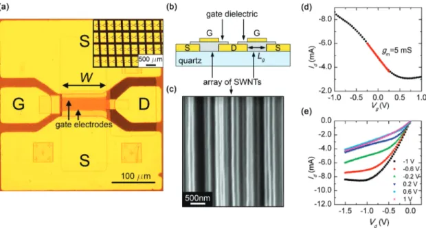
Figure 1a shows an optical micrograph of a characteristic device on a quartz substrate, which involves hundreds of perfectly aligned, SWNT in a linear array (at densities of 2 or 5 SWNTs/µm) grown by chemical vapor deposition (CVD).23-25 The device layout consists of two separately
fabricated parts: the probing pads and the active device. The active region was defined first. It employs a double channel configuration in which two gate electrodes and two source electrodes surround a common drain electrode. Fabrication involved two electron beam lithography (Raith, eLine) processes to define the source/drain and the gate levels with accurate registration to maximize the width of the gate and to minimize the capacitances associated with overlap between
the source/drain and the gate. A layer of HfO2 (50 nm)
deposited by electron beam evaporation (Temescal CV-8) served as the gate dielectric. Photolithography defined comparatively large probing pads that provided electrical contact to the smaller features of the active region. The configuration of the pads (3 nm Ti/100 nm Au), as defined by photolithography, matches that of conventional ground-signal-ground (GSG) microwave probes (150 µm pitch). Figure 1a,b presents an optical micrograph of a representative device and a cross sectional schematic illustration, respec-tively. An array of devices was formed in the manner described above (Figure 1a inset). These devices had channel lengths (Lg) between 900 and 300 nm and channel widths
(W) between 100 and 25 µm. The double channel geometry means that the total device width used for calculations is twice W. For the remainder of the text, W will be used for the purposes of discussion. DC performance was evaluated using conventional setups (Agilent E5270B Precision Mea-surement Mainframe). The source monitor units were con-nected through two Agilent 11612B bias networks to a pair of 150 µm pitch Picoprobe microwave probes, just prior to high-frequency measurements. Figure 1d,e shows transfer and output characteristics of a typical device (Lg) 700 nm;
W ) 100 µm; 5 SWNT/um), respectively. The devices show p channel behavior, with a moderate degree of ambipolar
operation as is often observed with top-gated SWNT transis-tors, either in array8or in single tube26formats. For the device
of Figure 1, the on-state current is∼8.5 mA at a drain bias (Vd) of -1 V. The peak transconductance (gm) is ∼5 mS
(25 mS/mm of channel width), at a drain bias of -1 V and gate bias (Vg) of 0 V. For the same bias, the output resistance,
Figure 1.Optical and scanning electron micrographs, cross sectional schematic illustration, and representative data from RF SWNT array transistors formed on a quartz substrate: (a) optical microscope images of a typical device and a collection of devices (inset) showing the RF probe pad configuration and double gate layout. The channel regions of the transistors were fabricated by two electron beam lithography processes; the contact pads with ground-signal-ground coplanar structure were formed by photolithography. The dark region at the center of the device shown in (a) is due to the gate dielectric (50nm thick HfO2). The channel width (W) and length (Lg) of this device are 100
µm and 700 nm, respectively. (b) Schematic cross sectional illustration of the device layout. (c) Scanning electron micrographs of aligned
SWNTs used for the fabricated devices. The nanotube density is 5 tubes/µm. (d) Transfer characteristics of the device shown in panel b, measured at a drain bias (Vd) of -1 V. (e) Output characteristics of this device, for gate voltages (Vg) between -1 and 1 V, measured in steps of 0.4 V.
Ro, is∼520 Ω, corresponding to a gain (G ) Rogm) of∼2.6.
With interdigitated devices, it is possible to reach high values of gm, up to 80 mS, and output currents, up to 0.1 A (Figure
S1, Supporting Information). In all cases, the ratio of the on-state to off-state current is close to three, due to the substantial (1/3) population of metallic nanotubes.
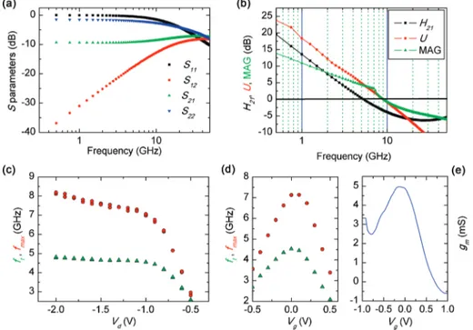
To determine the high-frequency behavior, we measured the S-parameters directly, using standard procedures with a vector network analyzer over a frequency range of 0.5-50 GHz (Agilent 8364A). Calibration was performed to the probe tips using off-wafer short-open-load-through (SOLT) standards on a GGB Industries CS-5 calibration substrate. Figure 2a shows the S-parameters for the device presented in Figure 1d,e. Figure 2b presents current gain (H21),
maximum available gain (MAG), and unilateral power gain (U ), all derived from the S-parameters at a drain bias of -1 V and gate bias of 0 V. The details of these conversions can be found in the Supporting Information. These results indicate a unity current gain frequency, ft, and a unity power
gain frequency, fmax, of 5 and 9 GHz, respectively; ft
corresponds to the frequency for which the drain and gate currents are equal, and thus, their ratio is unity. At this frequency the current gain, H21, crosses the 0 dB line. The
fmaxparameter is the maximum frequency of oscillation, and
it is determined by the point at which the unilateral power gain (U ) is equal to 0 dB. Figure 2c presents the dependence of ftand fmaxon drain bias. With increasing negative bias
(-0.5 to -0.9 V), both ftand fmaxincrease linearly until they
saturate at a drain bias of approximately -1 V, which corresponds to an electric field of∼5 kV/cm. This electric field approaches that needed to saturate the carrier velocity.27
Figure 2d presents the dependence of ftand fmaxon gate bias.
Both ft and fmax reach maximum values near Vg ≈ 0 V,
coinciding with the peak in gm (Figure 2e, from DC
measurements), as expected. If we assume that ft ≈ gm/
[2π(Cgs + Cgd)], where Cgs and Cgd are the capacitance
between the gate and source electrodes and the gate and drain electrodes, respectively,6,19then we estimate that C
gs+ Cgd
≈ 171 fF at the point of maximum gm. This expression is
reasonable when parasitic resistances are small relative to output resistance, which is the case (shown subsequently) for these devices.
Scaling studies provide additional information. Figure 3a,b shows the dependence of fmaxand ft, respectively, on Lgfor
two different device sets with average tube densities of∼2 SWNT/µm and 5 SWNT/µm, each with W ) 100 µm. Both
fmaxand ftincrease with decreasing Lg, qualitatively consistent
with expectation. The precise form of the scaling with channel length cannot be determined conclusively from these data. Some insights can, however, be obtained by noting that the transconductances determined from DC measurements (extracted in the same manner as Figure 2e), as well as those extracted through analysis of RF data (as described subse-quently) yield similar values, with only a weak dependence on Lg(Figure S2a, Supporting Information). This is possibly
due to the combined effects of contact resistance, near ballistic transport, and systematic shifts in threshold voltage that we observed to increasingly positive values with decreasing channel length. As a result, one can conclude that for these devices, increases in operating frequency with decreasing Lgresult mainly from decreases in gate
capaci-tances, Cgs and Cgd, rather than increases in gm, as is
Figure 2.RF characteristics of a SWNT array transistor whose DC characteristics appear in Figure 1: (a) amplitude plots of S-parameters for frequencies between 0.5 and 50 GHz; (b) amplitude plots for current gain (H21), unilateral power gain (U ), and maximum available gain (MAG) for frequencies between 0.5 and 50 GHz. The unity current gain frequency, ft, and unity power gain frequency, fmax, are around 5 and 9 GHz, respectively. (c) Plots of ftand fmaxas a function of drain bias (Vd) at a gate bias (Vg) of 0 V. (d) Plots of ftand fmaxas a function of Vg at Vd) -1 V. (e) Plot of transconductance, as calculated from the slope of transfer curve in Figure 1d, as function of Vg. The maximum frequencies and the peaks in transconductance appear at approximately the same Vg, as expected.
confirmed by the RF device analysis presented next. The scaling with W is as expected: gm, Cgs, and Cgdall increase
roughly linearly with increasing W (Figure S4, Supporting Information), thereby yielding values of ftthat are
indepen-dent of W, as shown in Figure 3c for devices with Lg) 700
nm and a density of∼2 SWNT/µm. Additional information can be obtained by examining the dependence of fton gm,
as shown in Figure 3d, derived from data collected at various
Vg (Figure 2d,e). The approximate linear scaling that is
observed over certain regions is consistent with values of
Cgs and Cgd that do not vary strongly with Vg, thereby
suggesting a relatively small contribution of the semicon-ducting tubes to the overall gate capacitance, as is confirmed through analysis described in the following.
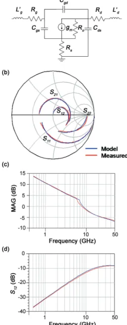
To understand more fully the nature of device operation, we used hybrid-pi models, common for two-port small-signal response in conventional transistor and circuit modeling, in which the behavior around a bias point is analyzed in the context of an equivalent circuit with linear physical quantities (such as capacitance, inductance, and resistance). For suf-ficiently small signal variations, the response of the circuit is assumed to be linear with a behavior consistent with this model. The main parameters for the model, which was implemented with commercial software tools designed for this purpose (Agilent Advanced Design System), are the output resistance (Ro), the transconductance (gm), the
induc-tances (L′) and resistances (R) of each of the metal electrodes (i.e., L′g, Rg, L′d, Rd, L′s, and Rs, where subscripts g, d, and
s refer to gate, drain, and source, respectively), and the capacitances between gate and drain (Cgd), gate and source
(Cgs), and drain and source (Cds). L′sis also set to zero due
to the minimal inductance expected based on the layout of the source electrode. The remaining parameters and their topology within the model are shown in Figure 4a. The modulation of the semiconducting tubes by the gate is represented by a voltage-controlled current source located between the source and drain.
In principle, the parameters extracted from analysis of such a model can provide physically meaningful characteristics of the devices. The relatively large number of variables (10) and the complex topology of the error surface associated with the fitting process, however, create difficulties. To reduce the number of free variables, we performed measurements on test structures with geometries exactly the same as those of the active devices but without the SWNTs and used information from these models as well as other techniques to constrain other parameters of the model. The test structures, which we refer to as “open” devices, were evaluated using the same frequency-dependent measurements as the active devices, and with similar models (parameters and topology in Figure S3a, Supporting Information), for the purpose of de-embedding and to evaluate the parasitic capacitances due only to the electrode geometry. An opti-mized fit of the data to a somewhat simpler model (eight free variables), shows good agreement (Figure S3b, Sup-porting Information), up to 20 GHz. The resulting parameters (Table S1, Supporting Information) provide information useful for fitting of data from the active devices. In particular, we can use the values of Rs, Rd, Rg, L′d, and L′gdetermined
from the open devices for modeling the active devices (the resistances are within a factor of 3 of values calculated using the electrode geometries and bulk resistivities;28Table S1,
Supporting Information). Although the capacitances from the “open” devices cannot be used in a similar manner, due to the absence of contributions from the SWNTs, they can be used with the results from the active device to yield insights
Figure 3.Variation of response frequencies ftand fmaxwith channel length (Lg) and channel width (W) and dependence of fton gm: (a, b) Plots of ftand fmaxevaluated at Vd) -2.5 V and Vg) 0 V as a function of Lgfor devices with W ) 100 µm; (c) Plot of ftat Vd ) -2.5 V and Vg) 0 V as a function of W for Lg) 700 nm. All devices here have a nanotube density of 2 SWNTs/µm. (d) Plot of
about the relative contributions to device capacitances, as described subsequently.
Further constraints can be imposed on the active device variables. For example, Cgdcan be obtained from the
single-pole roll off of S12(Figure 4d) with decreasing frequency.
At low frequencies Cgdis the dominant element determining
reverse feedback through the transistor; Cgd is manually
adjusted to make the modeled and measured S12 curves
coincide at 200 MHz. The output resistance was set to the DC value, Ro ) 520 Ω. Collectively, these considerations
allow for a reduction of the fitting variables from 10 to 3, by fixing Rs, Rd, Rg, Ro, L′d, L′g, and Cgd. We found that the
three remaining parameters could be determined reliably by fitting, independent of starting values, to within a few femtofarads (Cgsand Cds) and tenths of millisiemens (gm).
For the final optimization, the value of Cgd was adjusted
slightly following fitting of other parameters to improve the overall fit.
The final optimization yielded good fits to S-parameter data (Figure 4b,d) measured from the device discussed in Figures 1 and 2 over two decades of frequency, up to 50 GHz. The maximum available gain, which is derived from these S-parameters (Figure 4c), also shows excellent agree-ment. The values found for the optimization parameters appear in Table 1. As mentioned earlier, gmextracted from
RF analysis are similar to DC values (Figure 2e). The same model was used to evaluate the channel length (Figure S2, Supporting Information) and channel width (Figure S4, Supporting Information) scaling of parameters for the devices presented in Figure 3 with 2 SWNT/µm. In all cases, values of gm extracted in this manner correspond well to those
determined from DC measurements (also in Figure S2 and S4, Supporting Information), indicating no systematic varia-tion with channel length. The capacitances determined for the active device are similar to those for the open device (Table S1, Supporting Information), consistent with the conclusion that contributions due to semiconducting nano-tubes are relatively small compared with parasitics, as also suggested by the relationship between ftand gm(Figure 3d).
The value of Cgs+ Cgdfrom this RF analysis yields∼135
fF, which is comparable to that determined from direct measurements of ftand gmand the approximate relationship
between these quantities, as discussed previously. Parameters
Cgsand Cgdwere also found to scale with increasing channel
length and width (Figure S2 and S4, Supporting Information), as is expected with an increasing gate area. As mentioned previously, this scaling is most likely responsible for the trends observed in ft.
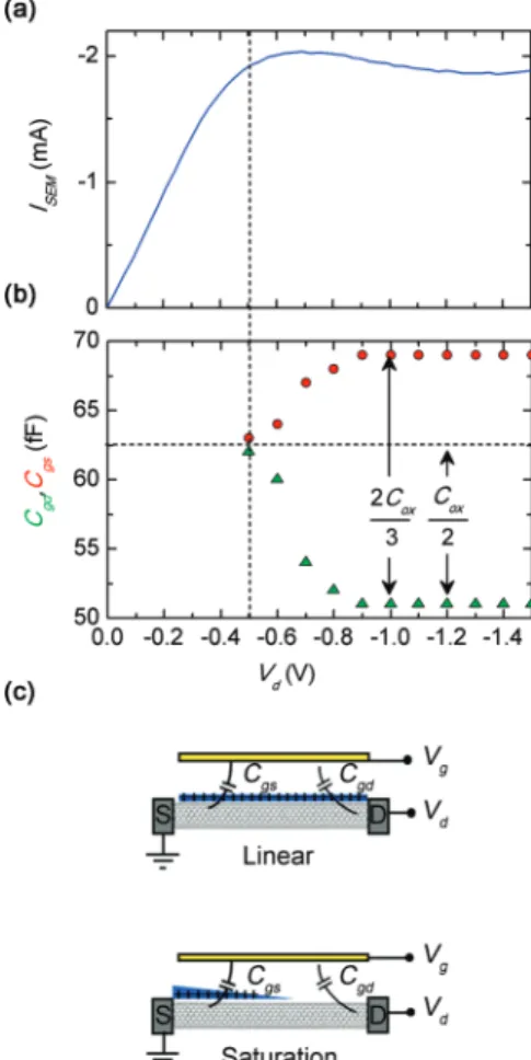
To gain additional insights into the capacitances, we examined their dependence on Vd.29 Because the devices
studied here operate in depletion mode, at small source/drain bias (e.g., -0.5 < Vd< 0 V), the devices are in the linear
response regime, such that we can assume that the charge distributions on the SWNTs are spatially symmetric. Figure 5a shows the output response due only to semiconducting SWNTs, generated by subtracting the current due to metallic SWNTs (i.e., the device in its off state). At high bias (e.g., -1.5 < Vd< -0.5 V), the devices are in saturation and the
charge distributions are asymmetric (Figure 5). Figure 5b shows Cgsand Cgd, extracted via fitting of RF data for the
device described in Figures 1 and 2, as described above, as a function of Vd. In the linear region, Cgsand Cgdhave similar
values, which we write as (Cp+ Cox)/2, where Cox is the
Figure 4.Measured and modeled RF response of a SWNT array transistor in a 50 Ω system with channel width (W) of 100 µm and a channel length (Lg) of 700 nm, biased at Vg) 0 and Vd) -1 V. The device here has a nanotube density of 5 SWNTs/µm. (a) Circuit schematic of the model, with key variables identified. (b) Smith chart of measured and simulated S-parameters. (c) Frequency dependence of MAG, the gain if the device were impedance matched. (d) Frequency dependence of S12, the reverse isolation. Here, the single-pole roll off with decreasing frequency is due to
Cgd. Cgdis directly extracted at low frequencies, in this case at 0.2 GHz.
Table 1. Values for Device Parameters Calculated from RF Modeling
L′g L′d Rg Rs Rd Ro Cgs Cgd Cds gm
pH pH Ω Ω Ω Ω fF fF fF mS
capacitance contribution associated with the coupling of the semiconducting tubes to the gate electrode and Cp is
associated with all other contributions (i.e., metallic tubes, fringing fields, overlaps, etc). In saturation, as the drain voltage is decreased, Cgddecreases, due to the asymmetry
of the charge distribution; the value of Cgd in this regime
gives Cp directly.29 By similar reasoning, Cgs increases to
2Cox/3 + Cpin saturation. This analysis yields the parasitic
capacitance, Cp ≈ 51 fF, and the gate oxide capacitance,
Cox≈ 22 fF. Calculations that include full effects of fringing
fields and screening of tubes in the arrays and the quantum capacitances, with device dimensions reported previously and a dielectric constant of∼14 for the HfO2, yield a computed
Coxof ∼30-40 fF for tube densities of 4-5 SWNTs/µm,
with negligible effects of nonuniform tube-tube spacings in the array. See Supporting Information for details. The quantity Cphas contributions from fringing fields between
the metal electrodes (Cf) and from the metallic SWNTs (Cm),
the latter of which we consider also as parasitic because these tubes contribute capacitance without contributing to gm. If
we assume a 2:1 ratio of semiconducting to metallic tubes,30
then the parasitic capacitance of the metallic tubes is Cm≈
10 fF, which yields Cf ≈ 40 fF. This value of fringing
capacitance is in the same range as values obtained by finite element modeling (∼55 fF, Figure S11, Supporting Informa-tion). These parameters, together with the carrier velocity (Vs), determine the intrinsic switching time of the device.
For a short channel device, the carrier velocity can be written as Vs ) gmLg/Cox. With parameters outlined above, this
equation yields Vs≈ 1.2 × 107cm/s, which agrees well with
previous reported values (∼2 × 107 cm/s).27The intrinsic
cutoff frequency can be evaluated by considering a device that is free of parasitics, such that ft) gm/(2πCox). Here we
find the intrinsic cutoff frequency to be∼30 GHz, which is at least 6 times higher than the measured devices, all of which are dominated by parasitics. This metric defines performance expected for a single nanotube transistor free of parasitics. In addition, it represents the upper limit achievable with array-based SWNT transistors with densities sufficiently high to eliminate the significance of the parasitics and with metallic SWNTs removed, thereby eliminating their contri-butions to capacitance.
In summary, we constructed high speed nanotube transistors from aligned arrays of hundreds of parallel nanotubes and assessed their performance by evaluating scattering parameters in the RF range. Interpretation of the results relied on small signal modeling of the RF response and on scaling analysis of properties in the DC and RF range. The results indicate that the gate capacitances, including significant contributions from parasitics for the devices examined here, have a dominant effect on the RF behavior and on ftand fmaxin particular. The relative
contributions to this capacitance by semiconducting and metallic nanotubes as well as fringing fields between device electrodes were assessed. Performance not limited by parasitics (not including those associated with metallic tubes) corresponds to the case where Cox. Cf. Devices that involve sufficiently high
densities of SWNTs can reach this regime. Further improve-ments (∼1.5× for the case when Cfis small) are possible by
eliminating the metallic tubes and, therefore, their contribution to capacitance. These two conclusions define goals for future work on growth and purification of arrays of SWNTs for applications in high speed electronics.
Acknowledgment. We thank K. Colravy for help with processing using facilities at the Frederick Seitz Materials Research Laboratory. This material is based upon work supported by the National Science Foundation (Grant NIRT-0403489), the U.S. Department of Energy (Grant DE-FG02-07ER46471), the Office of Naval Research via the National Defense Science and Engineering Graduate Fellowship, MITRE Corp., the Frederick Seitz Materials Research Laboratory, and the Center for Microanalysis of Materials (Grants DE-FG02-07ER46453 and DE-FG02-07ER46471) at the University of Illinois.
Supporting Information Available: Additional experi-mental and theoretical details. This material is available free of charge via the Internet at http://pubs.acs.org.
Figure 5. Capacitance contributions in SWNT array transistors: (a) Plot of drain current (Id) associated with the semiconducting SWNTs (i.e., Isem ) Id - Ioff where Ioff, the off state current, is associated with metallic tubes and is extracted from the minimum in current as a function of Vg) for a transistor with Lg) 700 nm at
Vg) 0 V as a function of drain voltage, Vd. The device saturates at a drain bias of Vd) -0.5 V. The device here has a nanotube density of 5 SWNT/µm. (b) Plot of Cgdand Cgs, extracted from RF modeling, as function of drain voltage. (c) Schematic representation of charge distribution on SWNT at linear and saturation regimes of behavior.
References
(1) Zhong, Z. H.; Gabor, N. M.; Sharping, J. E.; Gaeta, A. L.; McEuen, P. L. Nat. Nanotechnol. 2008, 3 (4), 201–205.
(2) Burke, P. J. Solid-State Electron. 2004, 48 (10-11), 1981–1986.
(3) Jing, G.; Hasan, S.; Javey, A.; Bosman, G.; Lundstrom, M. IEEE Trans.
Nanotechnol. 2005, 4 (6), 715–721.
(4) Ilani, S.; Donev, L. A. K.; Kindermann, M.; McEuen, P. L. Nat. Phys.
2006, 2 (10), 687–691.
(5) Saito, R.; Dresselhaus, G.; Dresselhaus, M. S. Physical Properties of
Carbon Nanotubes; Imperial College Press: London, 1998.
(6) Chau, R.; Datta, S.; Doczy, M.; Doyle, B.; Jin, B.; Kavalieros, J.; Majumdar, A.; Metz, M.; Radosavljevic, M. IEEE Trans. Nanotechnol.
2005, 4 (2), 153–158.
(7) Zhou, X. J.; Park, J. Y.; Huang, S. M.; Liu, J.; McEuen, P. L. Phys.
ReV. Lett. 2005, 95 (14), 4.
(8) Kang, S. J.; Kocabas, C.; Ozel, T.; Shim, M.; Pimparkar, N.; Alam, M. A.; Rotkin, S. V.; Rogers, J. A. Nat. Nanotechnol. 2007, 2 (4), 230–236.
(9) Baumgardner, J. E.; Pesetski, A. A.; Murduck, J. M.; Przybysz, J. X.; Adam, J. D.; Zhang, H. Appl. Phys. Lett. 2007, 91 (5), 052107.
(10) Kocabas, C.; Kim, H. S.; Banks, T.; Rogers, J. A.; Pesetski, A. A.; Baumgardner, J. E.; Krishnaswamy, S. V.; Zhang, H. Proc. Natl. Acad.
Sci. U.S.A. 2008, 105, 1405–1409.
(11) Pesetski, A. A.; Baumgardner, J. E.; Krishnaswamy, S. V.; Zhang, H.; Adam, J. D.; Kocabas, C.; Banks, T.; Rogers, J. A. Appl. Phys.
Lett. 2008, 93 (12), 123506.
(12) Cao, Q.; Kim, H. S.; Pimparkar, N.; Kulkarni, J. P.; Wang, C. J.; Shim, M.; Roy, K.; Alam, M. A.; Rogers, J. A. Nature 2008, 454 (7203), 495-U4.
(13) Chen, Z. H.; Appenzeller, J.; Lin, Y. M.; Sippel-Oakley, J.; Rinzler, A. G.; Tang, J. Y.; Wind, S. J.; Solomon, P. M.; Avouris, P. Science
2006, 311 (5768), 1735–1735.
(14) Bethoux, J. M.; Happy, H.; Dambrine, G.; Derycke, V.; Goffman, M.; Bourgoin, J. P. IEEE Electron DeVice Lett. 2006, 27 (8), 681– 683.
(15) Appenzeller, J.; Frank, D. J. Appl. Phys. Lett. 2004, 84 (10), 1771– 1773.
(16) Rosenblatt, S.; Lin, H.; Sazonova, V.; Tiwari, S.; McEuen, P. L. Appl.
Phys. Lett. 2005, 87 (15), 3.
(17) Wang, D.; Yu, Z.; McKernan, S.; Burke, P. J. IEEE Trans.
Nano-technol. 2007, 6 (4), 400–403.
(18) Chaste, J.; Lechner, L.; Morfin, P.; Feve, G.; Kontos, T.; Berroir, J. M.; Glattli, D. C.; Happy, H.; Hakonen, P.; Placais, B. Nano Lett. 2008,
8 (2), 525–528.
(19) Huo, X.; Zhang, M.; Chan, P. C. H.; Liang, Q.; Tang, Z. K. High frequency S parameters characterization of back-gate carbon nanotube field-effect transistors, Electron Devices Meeting, IEDM Technical Digest. IEEE International, 2004; pp 691-694.
(20) Chimot, N.; Derycke, V.; Goffman, M. F.; Bourgoin, J. P.; Happy, H.; Dambrine, G. Appl. Phys. Lett. 2007, 91 (15), 153111.
(21) Collin, R. E., Foundations for MicrowaVe Engineering, 2nd ed.; Wiley: Hoboken, NJ, 2001.
(22) Louarn, A. L.; Kapche, F.; Bethoux, J. M.; Happy, H.; Dambrine, G.; Derycke, V.; Chenevier, P.; Izard, N.; Goffman, M. F.; Bourgoin, J. P.
Appl. Phys. Lett. 2007, 90 (23), 233108.
(23) Kocabas, C.; Hur, S. H.; Gaur, A.; Meitl, M. A.; Shim, M.; Rogers, J. A. Small 2005, 1, 1110–1116.
(24) Kocabas, C.; Kang, S. J.; Ozel, T.; Shim, M.; Rogers, J. A. J. Phys.
Chem. C 2007, 111, 17879–17886.
(25) Kocabas, C.; Shim, M.; Rogers, J. A. J. Am. Chem. Soc. 2006, 128 (14), 4540–4541.
(26) Wind, S. J.; Appenzeller, J.; Martel, R.; Derycke, V.; Avouris, P. J.
Vac. Sci. Technol., B 2002, 20, 2798–2801.
(27) Chen, Y. F.; Fuhrer, M. S. Phys. ReV. Lett. 2005, 95 (23), 236803.
(28) Metals Handbook, 2nd ed.; ASM International: Materials Park, OH, 1998.
(29) Leaver, K., Microelectronic deVices, 2 ed.; World Scientific: London, 1997; p 138-140.
(30) Kocabas, C.; Pimparkar, N.; Yesilyurt, O.; Kang, S. J.; Alam, M. A.; Rogers, J. A. Nano Lett. 2007, 7, 1195–1202.